ICGOO在线商城 > 分立半导体产品 > 晶体管 - FET,MOSFET - 单 > STD4NS25T4

 Datasheet下载
- 型号: STD4NS25T4
- 制造商: STMicroelectronics
- 库位|库存: xxxx|xxxx
- 要求:
| 数量阶梯 | 香港交货 | 国内含税 |
| +xxxx | $xxxx | ¥xxxx |
查看当月历史价格
查看今年历史价格
STD4NS25T4产品简介:
ICGOO电子元器件商城为您提供STD4NS25T4由STMicroelectronics设计生产,在icgoo商城现货销售,并且可以通过原厂、代理商等渠道进行代购。 STD4NS25T4价格参考¥询价-¥询价。STMicroelectronicsSTD4NS25T4封装/规格:晶体管 - FET,MOSFET - 单, 表面贴装 N 沟道 250V 4A(Tc) 50W(Tc) DPAK。您可以下载STD4NS25T4参考资料、Datasheet数据手册功能说明书,资料中有STD4NS25T4 详细功能的应用电路图电压和使用方法及教程。
STMicroelectronics(意法半导体)的型号 STD4NS25T4 是一款N沟道增强型MOSFET,采用T4封装,常用于需要高效能开关和功率控制的场合。其主要应用场景包括:

1. 电源管理:用于DC-DC转换器、开关电源(SMPS)中,实现高效的能量转换,适用于笔记本电脑、服务器和工业电源系统。

2. 电机控制:在电动工具、家用电器和工业自动化设备中,作为电机驱动电路中的开关元件,实现对电机转速和方向的控制。

3. 负载开关:用于控制高功率负载的通断,如LED照明、加热元件或风扇,具有快速开关和低导通电阻的优点。

4. 逆变器与UPS系统:在不间断电源(UPS)和光伏逆变器中,用于将直流电转换为交流电,具备良好的热稳定性和高可靠性。

5. 汽车电子:适用于车载电源系统、电机驱动及车身控制模块,如车窗升降器、雨刷电机等,符合汽车级可靠性要求。

该器件具备低导通电阻、高耐压(250V)和良好热性能,适合高频开关应用,有助于减小系统体积并提高效率。
| 参数 | 数值 |
| 产品目录 | |
| 描述 | MOSFET N-CH 250V 4A DPAK |
| 产品分类 | FET - 单 |
| FET功能 | 标准 |
| FET类型 | MOSFET N 通道,金属氧化物 |
| 品牌 | STMicroelectronics |
| 数据手册 | |
| 产品图片 |
|
| 产品型号 | STD4NS25T4 |
| rohs | 无铅 / 符合限制有害物质指令(RoHS)规范要求 |
| 产品系列 | MESH OVERLAY™ |
| 不同Id时的Vgs(th)(最大值) | 4V @ 250µA |
| 不同Vds时的输入电容(Ciss) | 355pF @ 25V |
| 不同Vgs时的栅极电荷(Qg) | 27nC @ 10V |
| 不同 Id、Vgs时的 RdsOn(最大值) | 1.1 欧姆 @ 2A,10V |
| 产品目录页面 | |
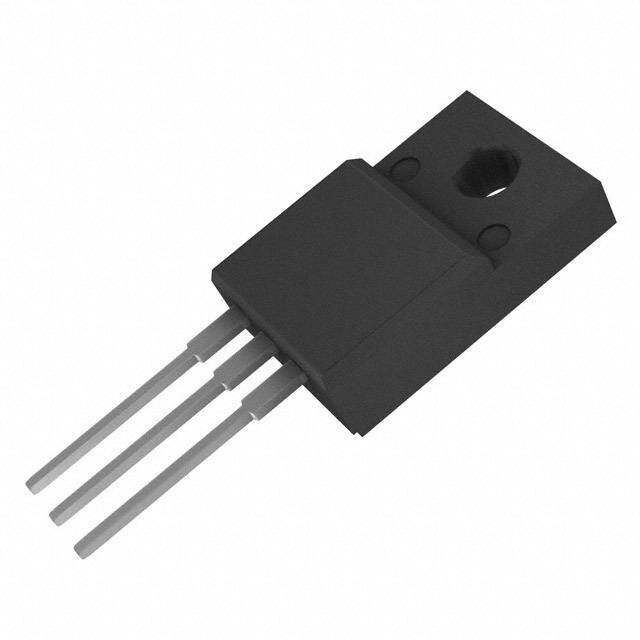
| 供应商器件封装 | D-Pak |
| 其它名称 | 497-8479-1 |
| 功率-最大值 | 50W |
| 包装 | 剪切带 (CT) |
| 安装类型 | 表面贴装 |
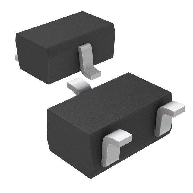
| 封装/外壳 | TO-252-3,DPak(2 引线+接片),SC-63 |
| 标准包装 | 1 |
| 漏源极电压(Vdss) | 250V |
| 电流-连续漏极(Id)(25°C时) | 4A (Tc) |


.jpg)


- 商务部:美国ITC正式对集成电路等产品启动337调查
- 曝三星4nm工艺存在良率问题 高通将骁龙8 Gen1或转产台积电
- 太阳诱电将投资9.5亿元在常州建新厂生产MLCC 预计2023年完工
- 英特尔发布欧洲新工厂建设计划 深化IDM 2.0 战略
- 台积电先进制程称霸业界 有大客户加持明年业绩稳了
- 达到5530亿美元!SIA预计今年全球半导体销售额将创下新高
- 英特尔拟将自动驾驶子公司Mobileye上市 估值或超500亿美元
- 三星加码芯片和SET,合并消费电子和移动部门,撤换高东真等 CEO
- 三星电子宣布重大人事变动 还合并消费电子和移动部门
- 海关总署:前11个月进口集成电路产品价值2.52万亿元 增长14.8%


PDF Datasheet 数据手册内容提取
STD4NS25 W N-CHANNEL 250V - 0.9 - 4A DPAK/IPAK MESH OVERLAY™ MOSFET TYPE VDSS RDS(on) ID STD4NS25 250 V < 1.1 W 4 A n TYPICAL RDS(on) = 0.9 W ) n EXTREMELY HIGH dv/dt CAPABILITY 3 s 3 n 100% AVALANCHE TESTED t( 2 ADD SUFFIX “T4” FOR ORDERING IN TAPE & 1 c 1 n u REEL d DPAK o IPAK DESCRIPTION TO-252 P r TO-251 Using the latest high voltage MESH OVERLAY™ e process, STMicroelectronics has designed an ad- t vanced family of power MOSFETs with outstanding e performance. The new patented STrip layout cou- ol pled with the Company’s proprietary edge termina- s tion structure, makes it suitable in coverters for b INTERNAL SCHEMATIC DIAGRAM lighting applications. O - ) s APPLICATIONS ( t HIGH CURRENT, HIGH SPEED cSWITCHING n u SWITH MODE POWER SUPPLIES (SMPS) n d n DC-DC CONVERTERS oFOR TELECOM, INDUSTRIAL, AND LrIGHTING EQUIPMENT P e t e l o s ABSOLUTE MAXIMUM RATINGS b O Symbol Parameter Value Unit VDS Drain-source Voltage (VGS = 0) 250 V VDGR Drain-gate Voltage (RGS = 20 kW ) 250 V VGS Gate- source Voltage ± 20 V ID Drain Current (continuos) at TC = 25°C 4 A ID Drain Current (continuos) at TC = 100°C 2.5 A IDM (l) Drain Current (pulsed) 16 A PTOT Total Dissipation at TC = 25°C 50 W Derating Factor 0.4 W/°C dv/dt (1) Peak Diode Recovery voltage slope 5 V/ns Tstg Storage Temperature –65 to 150 °C Tj Max. Operating Junction Temperature 150 °C (•)Pulse width limited by safe operating area (1) ISD £ 4A, di/dt£ 300 A/m s, VDD£ V(BR)DSS, Tj£ TjMAX February 2001 1/9
STD4NS25 THERMAL DATA Rthj-case Thermal Resistance Junction-case Max 2.5 °C/W Rthj-amb Thermal Resistance Junction-ambient Max 100 °C/W Rthc-sink Thermal Resistance Case-sink Typ 1.5 °C/W Tl Maximum Lead Temperature For Soldering Purpose 275 °C AVALANCHE CHARACTERISTICS Symbol Parameter Max Value Unit IAR Avalanche Current, Repetitive or Not-Repetitive 4 A (pulse width limited by Tj max) EAS Single Pulse Avalanche Energy 120 )mJ (starting Tj = 25 °C, ID = IAR, VDD = 50 V) s ( t c ELECTRICAL CHARACTERISTICS (TCASE = 25 °C UNLESS OTHERWISE SPECIFIED) u OFF d Symbol Parameter Test Conditions Min. oTyp. Max. Unit r V(BR)DSS Drain-source ID = 250 µA, VGS = 0 250P V Breakdown Voltage e IDSS Zero Gate Voltage VDS = Max Rating e t 1 µA Drain Current (VGS = 0) VDS = Max Rating, TC o= l125 °C 10 µA IGSS Gate-body Leakage VGS = ±20V s ±100 nA b Current (VDS = 0) O - ON (1) ) s Symbol Parameter ( Test Conditions Min. Typ. Max. Unit t VGS(th) Gate Threshold Voltage c VDS = VGS, ID = 250µA 2 3 4 V u RDS(on) Static Drain-sourced On VGS = 10V, ID = 2 A 0.9 1.1 W Resistance o r P ID(on) On State Drain Current VDS > ID(on) x RDS(on)max, 4 A e VGS=10V t e l DYNAMoIC s b Symbol Parameter Test Conditions Min. Typ. Max. Unit O gfs (1) Forward Transconductance VDS > ID(on) x RDS(on)max, 1 3.5 S ID=2A Ciss Input Capacitance VDS = 25V, f = 1 MHz, VGS = 0 355 pF Coss Output Capacitance 64 pF Reverse Transfer Crss Capacitance 29.5 pF 2/9
STD4NS25 ELECTRICAL CHARACTERISTICS (CONTINUED) SWITCHING ON Symbol Parameter Test Conditions Min. Typ. Max. Unit td(on) Turn-on Delay Time VDD = 125 V, ID = 2 A 12 ns RG=4.7W VGS = 10 V tr Rise Time (see test circuit, Figure 3) 18 ns Qg Total Gate Charge VDD = 200V, ID = 4 A, 19 27 nC Qgs Gate-Source Charge VGS = 10V 3.2 nC Qgd Gate-Drain Charge 7.5 nC ) SWITCHING OFF s ( Symbol Parameter Test Conditions Min. Typ. Matx. Unit c td(Voff) Turn-off- Delay Time VDD = 125V, ID = 2 A, 70 u ns tf Fall Time RG=4.7W, VGS = 10V 10.5d ns o (see test circuit, Figure 3) r tr(Voff) Off-voltage Rise Time Vclamp = 200V, ID = 4 A, P 13 ns tf Fall Time RG=4.7W, VGS = 10V e 10 ns tc Cross-over Time (see test circuit, Figure 5) t 21.5 ns e l o SOURCE DRAIN DIODE s b Symbol Parameter Test Conditions Min. Typ. Max. Unit O ISD Source-drain Current 4 A - ISDM (2) Source-drain Current (pulsed) ) 16 A s VSD (1) Forward On Voltage ( ISD = 4 A, VGS = 0 1.5 V t trr Reverse Recovery Timec ISD = 4 A, di/dt = 100A/µs 124 ns u Qrr Reverse Recoveryd Charge VDD = 30V, Tj = 150°C 0.5 m C (see test circuit, Figure 5) o IRRM Reverse Rercovery Current 7.2 A P Note: 1. Pulsed: Pulse duration = 300 µs, duty cycle 1.5 %. 2. Pulse width elim ited by safe operating area. t Safe Opereating Area Thermal Impedance l o s b O 3/9
STD4NS25 Output Characteristics Transfer Characteristics ) s ( t c u d o r P Transconductance Static Drain-sou rce On Resistance e t e l o s b O - ) s ( t c u d o r P e t e l o s Gate Charge vs Gate-source Voltage Capacitance Variations b O 4/9
STD4NS25 Normalized Gate Thereshold Voltage vs Temp. Normalized On Resistance vs Temperature ) s ( t c u d o r P Source-drain Diode Forward Characteristics e t e l o s b O - ) s ( t c u d o r P e t e l o s b O 5/9
STD4NS25 Fig. 1: Unclamped Inductive Load Test Circuit Fig. 2: Unclamped Inductive Waveform ) s ( t c u d o r P Fig. 3: Switching Times Test Circuit For Fig. 4: Gate Charge test Circuit Resistive Load e t e l o s b O - ) s ( t c u d o r P e t e l o Fig. s5: Test Circuit For Inductive Load Switching Abnd Diode Recovery Times O 6/9
STD4NS25 TO-252 (DPAK) MECHANICAL DATA mm inch DIM. MIN. TYP. MAX. MIN. TYP. MAX. A 2.20 2.40 0.087 0.094 A1 0.90 1.10 0.035 0.043 A2 0.03 0.23 0.001 0.009 s ) ( B 0.64 0.90 0.025 0t.035 c B2 5.20 5.40 0.204 u 0.213 d C 0.45 0.60 0.018 0.024 o C2 0.48 0.60 0.019 r 0.024 P D 6.00 6.20 0.236 0.244 e E 6.40 6.60 0.25t2 0.260 e G 4.40 4.60 ol0.173 0.181 s H 9.35 10.10 0.368 0.398 b L2 0.8 O 0.031 L4 0.60 - 1.00 0.024 0.039 V2 0o ) 8o 0o 0o s ( t c u d o r P e t e l o s b O P032P_B 7/9
STD4NS25 TO-251 (IPAK) MECHANICAL DATA mm inch DIM. MIN. TYP. MAX. MIN. TYP. MAX. A 2.2 2.4 0.086 0.094 A1 0.9 1.1 0.035 0.043 A3 0.7 1.3 0.027 0.051 ) B 0.64 0.9 0.025 0.031 s ( B2 5.2 5.4 0.204 0.2t12 c B3 0.85 u 0.033 B5 0.3 0.012 d o B6 0.95 0.037 r C 0.45 0.6 0.017 P 0.023 C2 0.48 0.6 0.019 e 0.023 D 6 6.2 0.236t 0.244 e E 6.4 6.6 l0.252 0.260 o G 4.4 4.6 s 0.173 0.181 b H 15.9 16.3 0.626 0.641 O L 9 9.4 0.354 0.370 L1 0.8 - 1.2 0.031 0.047 ) L2 0.8 s 1 0.031 0.039 ( t c u d H o P r C e A t le C2 A3 o s 1 A b O L2 D L B3 B6 B B5 3 E = B2 = 2 G = = = = 1 L1 0068771-E 8/9
STD4NS25 ) s ( t c u d o r P e t e l o s b O - ) s ( t c u d o r P e t e l o s b O Information furnished is believed to be accurate and reliable. However, STMicroelectronics assumes no responsibility for the consequences of use of such information nor for any infringement of patents or other rights of third parties which may result from its use. No license is granted by implication or otherwise under any patent or patent rights of STMicroelectronics. Specification mentioned in this publication are subject to change without notice. This publication supersedes and replaces all information previously supplied. STMicroelectronics products are not authorized for use as critical components in life support devices or systems without express written approval of STMicroelectronics. The ST logo is a trademark of STMicroelectronics © 2000 STMicroelectronics – Printed in Italy – All Rights Reserved STMicroelectronics GROUP OF COMPANIES Australia - Brazil - China - Finland - France - Germany - Hong Kong - India - Italy - Japan - Malaysia - Malta - Morocco - Singapore - Spain - Sweden - Switzerland - United Kingdom - U.S.A. http://www.st.com 9/9