ICGOO在线商城 > 分立半导体产品 > 晶体管 - FET,MOSFET - 单 > SI1403BDL-T1-E3
 Datasheet下载
- 型号: SI1403BDL-T1-E3
- 制造商: Vishay
- 库位|库存: xxxx|xxxx
- 要求:
| 数量阶梯 | 香港交货 | 国内含税 |
| +xxxx | $xxxx | ¥xxxx |
查看当月历史价格
查看今年历史价格
SI1403BDL-T1-E3产品简介:
ICGOO电子元器件商城为您提供SI1403BDL-T1-E3由Vishay设计生产,在icgoo商城现货销售,并且可以通过原厂、代理商等渠道进行代购。 SI1403BDL-T1-E3价格参考。VishaySI1403BDL-T1-E3封装/规格:晶体管 - FET,MOSFET - 单, 表面贴装 P 沟道 20V 1.4A(Ta) 568mW(Ta) SC-70-6(SOT-363)。您可以下载SI1403BDL-T1-E3参考资料、Datasheet数据手册功能说明书,资料中有SI1403BDL-T1-E3 详细功能的应用电路图电压和使用方法及教程。
Vishay Siliconix 的 SI1403BDL-T1-E3 是一款 P 沟道增强型 MOSFET,属于晶体管中的场效应管(FET),常用于低电压、小功率的开关与控制应用。其主要应用场景包括便携式电子设备和电源管理电路。

该器件广泛应用于智能手机、平板电脑、可穿戴设备等消费类电子产品中,主要用于电源开关、负载开关、电池供电切换以及信号通断控制。由于其导通电阻低(Rds(on) 典型值较小),在低电压(如 3.3V 或 5V)系统中能有效减少功耗和发热,提高能效。

SI1403BDL-T1-E3 采用小型 SOT-23 封装,体积小巧,适合高密度 PCB 设计,特别适用于空间受限的便携设备。此外,它还可用于直流电机驱动、LED 控制、热插拔保护电路及各类逻辑电平转换电路中。

凭借 Vishay Siliconix 在半导体领域的可靠品质,该 MOSFET 具有良好的稳定性和耐用性,适用于工业控制、通信模块和家用电器中的低功率开关场景。总体而言,SI1403BDL-T1-E3 是一款高效、紧凑且可靠的 P 沟道 MOSFET,适用于多种低压、低功耗的开关控制应用。
| 参数 | 数值 |
| 产品目录 | |
| ChannelMode | Enhancement |
| 描述 | MOSFET P-CH 20V 1.4A SC70-6MOSFET 20V 1.5A |
| 产品分类 | FET - 单分离式半导体 |
| FET功能 | 逻辑电平门 |
| FET类型 | MOSFET P 通道,金属氧化物 |
| Id-ContinuousDrainCurrent | 1.4 A |
| Id-连续漏极电流 | 1.4 A |
| 品牌 | Vishay SiliconixVishay / Siliconix |
| 产品手册 | |
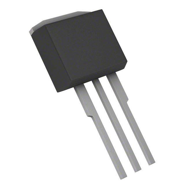
| 产品图片 |
|
| rohs | 符合RoHS无铅 / 符合限制有害物质指令(RoHS)规范要求 |
| 产品系列 | 晶体管,MOSFET,Vishay / Siliconix SI1403BDL-T1-E3TrenchFET® |
| 数据手册 | |
| 产品型号 | SI1403BDL-T1-E3SI1403BDL-T1-E3 |
| Pd-PowerDissipation | 568 mW |
| Pd-功率耗散 | 568 mW |
| RdsOn-Drain-SourceResistance | 150 mOhms |
| RdsOn-漏源导通电阻 | 150 mOhms |
| Vds-Drain-SourceBreakdownVoltage | 20 V |
| Vds-漏源极击穿电压 | - 20 V |
| Vgs-Gate-SourceBreakdownVoltage | +/- 12 V |
| Vgs-栅源极击穿电压 | 12 V |
| 上升时间 | 30 ns |
| 下降时间 | 30 ns |
| 不同Id时的Vgs(th)(最大值) | 1.3V @ 250µA |
| 不同Vds时的输入电容(Ciss) | - |
| 不同Vgs时的栅极电荷(Qg) | 4.5nC @ 4.5V |
| 不同 Id、Vgs时的 RdsOn(最大值) | 150 毫欧 @ 1.5A,4.5V |
| 产品目录页面 | |
| 产品种类 | MOSFET |
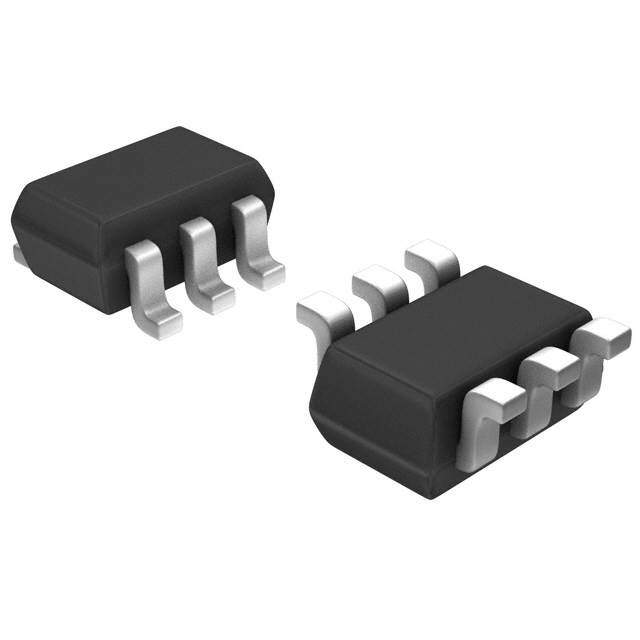
| 供应商器件封装 | SC-70-6 (SOT-363) |
| 其它名称 | SI1403BDL-T1-E3DKR |
| 典型关闭延迟时间 | 28 ns |
| 功率-最大值 | 568mW |
| 包装 | Digi-Reel® |
| 商标 | Vishay / Siliconix |
| 商标名 | TrenchFET |
| 安装类型 | 表面贴装 |
| 安装风格 | SMD/SMT |
| 封装 | Reel |
| 封装/外壳 | 6-TSSOP,SC-88,SOT-363 |
| 封装/箱体 | SOT-363-6 |
| 工厂包装数量 | 3000 |
| 晶体管极性 | P-Channel |
| 最大工作温度 | + 150 C |
| 最小工作温度 | - 55 C |
| 标准包装 | 1 |
| 漏源极电压(Vdss) | 20V |
| 电流-连续漏极(Id)(25°C时) | 1.4A (Ta) |
| 通道模式 | Enhancement |
| 配置 | Single |
| 零件号别名 | SI1403BDL-E3 |


- 商务部:美国ITC正式对集成电路等产品启动337调查
- 曝三星4nm工艺存在良率问题 高通将骁龙8 Gen1或转产台积电
- 太阳诱电将投资9.5亿元在常州建新厂生产MLCC 预计2023年完工
- 英特尔发布欧洲新工厂建设计划 深化IDM 2.0 战略
- 台积电先进制程称霸业界 有大客户加持明年业绩稳了
- 达到5530亿美元!SIA预计今年全球半导体销售额将创下新高
- 英特尔拟将自动驾驶子公司Mobileye上市 估值或超500亿美元
- 三星加码芯片和SET,合并消费电子和移动部门,撤换高东真等 CEO
- 三星电子宣布重大人事变动 还合并消费电子和移动部门
- 海关总署:前11个月进口集成电路产品价值2.52万亿元 增长14.8%


PDF Datasheet 数据手册内容提取
Si1403BDL New Product Vishay Siliconix P-Channel 2.5-V (G-S) MOSFET FEATURES PRODUCT SUMMARY (cid:1) TrenchFET(cid:2) Power MOSFET VDS (V) rDS(on) ((cid:1)) ID (A) Qg (Typ) 0.150 @ VGS = −4.5 V −1.5 −20 0.175 @ VGS = −3.6 V −1.4 2.9 0.265 @ VGS = −2.5 V −1.2 SOT-363 SC-70 (6-LEADS) D 1 6 D Marking Code D 2 5 D OD XXY Y Lot Traceability and Date Code G 3 4 S Part # Code Top View Ordering Information: Si1403BDL-T1—E3 ABSOLUTE MAXIMUM RATINGS (T = 25(cid:3)C UNLESS OTHERWISE NOTED) A Parameter Symbol 5 secs Steady State Unit Drain-Source Voltage VDS −20 VV Gate-Source Voltage VGS (cid:1)12 TA = 25(cid:3)C −1.5 −1.4 CCoonnttiinnuuoouuss DDrraaiinn CCuurrrreenntt ((TTJJ == 115500(cid:3)(cid:3)CC))aa IIDD TA = 85(cid:3)C −1.2 −1.0 AA Pulsed Drain Current IDM −5 Continuous Diode Current (Diode Conduction)a IS −0.8 −0.8 TA = 25(cid:3)C 0.625 0.568 MMaaxxiimmuumm PPoowweerr DDiissssiippaattiioonnaa TA = 85(cid:3)C PPDD 0.400 0.295 WW Operating Junction and Storage Temperature Range TJ, Tstg −55 to 150 (cid:3)C THERMAL RESISTANCE RATINGS Parameter Symbol Typical Maximum Unit t (cid:2) 5 sec 165 200 MMaxiimum JJuncttiion-tto-AAmbbiienttaa Steady State RRthJA 180 220 (cid:3)CC//WW Maximum Junction-to-Foot (Drain) Steady State RthJF 105 130 Notes a. Surface Mounted on 1” x 1” FR4 Board. Document Number: 73253 www.vishay.com S-50137—Rev. A, 24-Jan-05 1
Si1403BDL Vishay Siliconix New Product SPECIFICATIONS (T = 25(cid:3)C UNLESS OTHERWISE NOTED) J Parameter Symbol Test Condition Min Typ Max Unit Static Gate Threshold Voltage VGS(th) VDS = VGS, ID = −250 (cid:2)A −0.6 −1.3 V Gate-Body Leakage IGSS VDS = 0 V, VGS = (cid:1)12 V (cid:1)100 nA ZZeerroo GGaattee VVoollttaaggee DDrraaiinn CCuurrrreenntt IIDDSSSS VDS =V −D2S0 = V −, V20G SV ,= V 0G SV ,= T 0J =V 85(cid:3)C −−15 (cid:2)(cid:2)AA On-State Drain Currenta ID(on) VDS = −5 V, VGS = −4.5 V −2 A VGS = −4.5 V, ID = −1.5 A 0.120 0.150 DDrraaiinn-SSoouurrccee OOnn-SSttaattee RReessiissttaanncceea rrDDSS((oonn)) VGS = −3.6 V, ID = −1.4 A 0.140 0.175 (cid:1)(cid:1) VGS = −2.5 V, ID = −0.8 A 0.220 0.265 Forward Transconductancea gfs VDS = −10 V, ID = −1.5 A 3.4 S Diode Forward Voltagea VSD IS = −0.8 A, VGS = 0 V −0.8 −1.1 V Dynamicb Total Gate Charge Qg 2.9 4.5 Gate-Source Charge Qgs VDDSS = −10 V,, VGGSS = −4.5 V,, IDD = −1.5 A 0.65 nC Gate-Drain Charge Qgd 1.0 Gate Resistance Rg f = 1.0 MHz 9 (cid:1) Turn-On Delay Time td(on) 13 20 Rise Time tr VVDDDD == −−1100 VV,, RRLL == 1100 (cid:1)(cid:1) 30 45 Turn-Off Delay Time td(off) ID (cid:3) −1 A, VGEN = −4.5 V, Rgg = 6 (cid:1) 28 42 nnss Fall Time tf 13 20 SBooduyrc De-ioDdraei nR eRveevresres eR eRceocvoevreyr yC hTaimrgee Qtrrrr IIFF == −00.88 AA, ddii//ddtt == 110000 AA//(cid:2)(cid:2)ss 142 285 nC Notes a. Pulse test; pulse width (cid:2) 300 (cid:2)s, duty cycle (cid:2) 2%. b. Guaranteed by design, not subject to production testing. Stresses beyond those listed under “Absolute Maximum Ratings” may cause permanent damage to the device. These are stress ratings only, and functional operation of the device at these or any other conditions beyond those indicated in the operational sections of the specifications is not implied. Exposure to absolute maximum rating conditions for extended periods may affect device reliability. TYPICAL CHARACTERISTICS (25(cid:3)C UNLESS NOTED) Output Characteristics Transfer Characteristics 4.0 4.0 TC = −55(cid:3)C VGS = 5 thru 2.5 V 25(cid:3)C 3.2 3.2 A) A) 125(cid:3)C nt ( 2.4 nt ( 2.4 urre 2 V urre C C n n ai 1.6 ai 1.6 Dr Dr − − D D I 0.8 I 0.8 1.5 V 1, 0.5 V 0.0 0.0 0.0 0.8 1.6 2.4 3.2 4.0 0.0 0.5 1.0 1.5 2.0 2.5 3.0 VDS − Drain-to-Source Voltage (V) VGS − Gate-to-Source Voltage (V) www.vishay.com Document Number: 73253 2 S-50137—Rev. A, 24-Jan-05
Si1403BDL New Product Vishay Siliconix TYPICAL CHARACTERISTICS (25(cid:3)C UNLESS NOTED) On-Resistance vs. Drain Current Capacitance 0.40 500 ) (cid:1) 0.32 400 ance ( VGS = 2.5 V e (pF) sist 0.24 anc 300 Ciss Re cit n- pa O a − 0.16 VGS = 3.6 V − C 200 n) C o S( rD 0.08 VGS = 4.5 V 100 Coss Crss 0.00 0 0 1 2 3 4 0 4 8 12 16 20 ID − Drain Current (A) VDS − Drain-to-Source Voltage (V) Gate Charge On-Resistance vs. Junction Temperature 5 1.6 ge (V) 4 VIDD =S 1=. 51 0A V 1.4 VIDG =S 1=. 54 .A5 V a e Volt ance − Gate-to-Sourc 23 − On-ResiistS(on)(Normalized) 11..02 GS rD V 1 0.8 0 0.6 0.0 0.5 1.0 1.5 2.0 2.5 3.0 −50 −25 0 25 50 75 100 125 150 Qg − Total Gate Charge (nC) TJ − Junction Temperature ((cid:3)C) Source-Drain Diode Forward Voltage On-Resistance vs. Gate-to-Source Voltage 10 0.40 TJ = 150(cid:3)C 0.35 ) (cid:1) nt (A) nce ( 0.30 e Curre 1 Resista 00..2205 ID = 0.8 A ID = 1.5 A − SourcS TJ = 25(cid:3)C − On-on) 0.15 I S( 0.10 D r 0.05 0.1 0.00 0.0 0.3 0.6 0.9 1.2 1.5 0 1 2 3 4 5 VSD − Source-to-Drain Voltage (V) VGS − Gate-to-Source Voltage (V) Document Number: 73253 www.vishay.com S-50137—Rev. A, 24-Jan-05 3
Si1403BDL Vishay Siliconix New Product TYPICAL CHARACTERISTICS (25(cid:3)C UNLESS NOTED) Threshold Voltage Single Pulse Power, Junction-to-Ambient 0.5 10 0.4 8 0.3 ID = 250 (cid:2)A V) nce ( 0.2 W) 6 Varia 0.1 wer ( S(th) −0.0 Po 4 G V −0.1 2 −0.2 −0.3 0 −50 −25 0 25 50 75 100 125 150 10−2 10−1 1 10 100 TJ − Temperature ((cid:3)C) Time (sec) Safe Operating Area 10 10 (cid:2)s *Limited by rDS(on) 100 (cid:2)s 1 ms 1 A) nt ( 10 ms e Curr 0.1 n 100 ms ai Dr 1 s, 100 s, dc − D I 0.01 TA = 25(cid:3)C Single Pulse 0.001 0.1 1 10 100 VDS − Drain-to-Source Voltage (V) *VGS (cid:4) minimum VGS at which rDS(on) is specified Normalized Thermal Transient Impedance, Junction-to-Ambient 2 1 nt Duty Cycle = 0.5 e ctive Transimpedance 0.2 Notes: ed Effeermal I 0.1 0.1 PDM malizTh 0.05 t1 Nor 0.02 1. Duty Cyclet,2 D = t1 2. Per Unit Base = RthtJ2A = 180(cid:3)C/W Single Pulse 3. TJM − TA = PDMZthJA(t) 4. Surface Mounted 0.01 10−4 10−3 10−2 10−1 1 10 100 600 Square Wave Pulse Duration (sec) www.vishay.com Document Number: 73253 4 S-50137—Rev. A, 24-Jan-05
Si1403BDL New Product Vishay Siliconix TYPICAL CHARACTERISTICS (25(cid:3)C UNLESS NOTED) Normalized Thermal Transient Impedance, Junction-to-Foot 2 1 nt Duty Cycle = 0.5 e ctive Transimpedance 0.2 zed Effehermal I 0.1 00..105 aliT m or 0.02 N Single Pulse 0.01 10−4 10−3 10−2 10−1 1 10 Square Wave Pulse Duration (sec) Vishay Siliconix maintains worldwide manufacturing capability. Products may be manufactured at one of several qualified locations. Reliability data for Silicon Technology and Package Reliability represent a composite of all qualified locations. For related documents such as package/tape drawings, part marking, and reliability data, see http://www.vishay.com/ppg?73253. Document Number: 73253 www.vishay.com S-50137—Rev. A, 24-Jan-05 5
Legal Disclaimer Notice Vishay Notice Specifications of the products displayed herein are subject to change without notice. Vishay Intertechnology, Inc., or anyone on its behalf, assumes no responsibility or liability for any errors or inaccuracies. Information contained herein is intended to provide a product description only. No license, express or implied, by estoppel or otherwise, to any intellectual property rights is granted by this document. Except as provided in Vishay's terms and conditions of sale for such products, Vishay assumes no liability whatsoever, and disclaims any express or implied warranty, relating to sale and/or use of Vishay products including liability or warranties relating to fitness for a particular purpose, merchantability, or infringement of any patent, copyright, or other intellectual property right. The products shown herein are not designed for use in medical, life-saving, or life-sustaining applications. Customers using or selling these products for use in such applications do so at their own risk and agree to fully indemnify Vishay for any damages resulting from such improper use or sale. Document Number: 91000 www.vishay.com Revision: 08-Apr-05 1
Mouser Electronics Authorized Distributor Click to View Pricing, Inventory, Delivery & Lifecycle Information: V ishay: SI1403BDL-T1-E3