ICGOO在线商城 > 分立半导体产品 > 晶体管 - FET,MOSFET - 射频 > CGH40025F
 Datasheet下载
- 型号: CGH40025F
- 制造商: Cree
- 库位|库存: xxxx|xxxx
- 要求:
| 数量阶梯 | 香港交货 | 国内含税 |
| +xxxx | $xxxx | ¥xxxx |
查看当月历史价格
查看今年历史价格
CGH40025F产品简介:
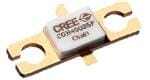
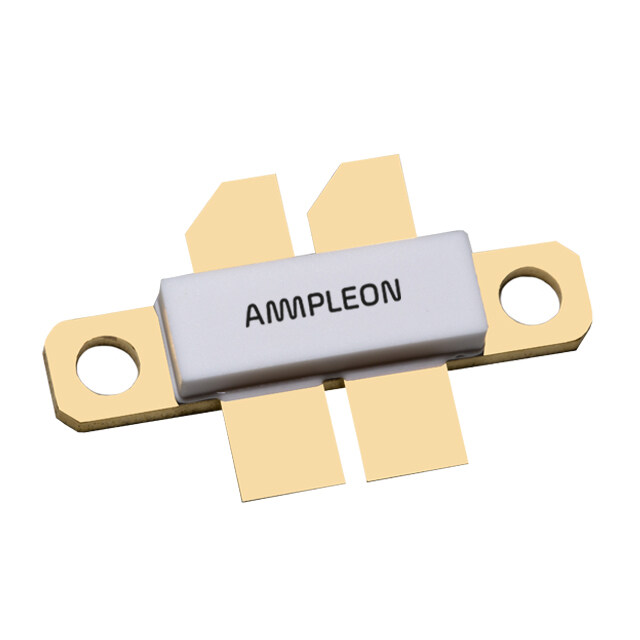
ICGOO电子元器件商城为您提供CGH40025F由Cree设计生产,在icgoo商城现货销售,并且可以通过原厂、代理商等渠道进行代购。 CGH40025F价格参考。CreeCGH40025F封装/规格:晶体管 - FET,MOSFET - 射频, 射频 Mosfet HEMT 28V 250mA 0Hz ~ 6GHz 13dB 30W 440166。您可以下载CGH40025F参考资料、Datasheet数据手册功能说明书,资料中有CGH40025F 详细功能的应用电路图电压和使用方法及教程。
Cree/Wolfspeed 的 CGH40025F 是一款基于氮化镓(GaN)高电子迁移率晶体管(HEMT)的射频功率MOSFET,广泛应用于高频、高效率、高功率场景。其主要应用场景包括:

1. 无线通信基站:适用于4G LTE、5G等移动通信基础设施中的宏基站和微波回传系统,工作频率可达2.5 GHz以下,提供高输出功率和优良的线性度,提升信号覆盖与传输质量。

2. 雷达系统:用于军用及民用雷达,如空中交通管制、气象雷达和相控阵雷达。CGH40025F具备高脉冲功率能力和良好热稳定性,适合在严苛环境下长时间运行。

3. 工业与科学设备:应用于射频加热、等离子体生成、医疗设备(如MRI射频激励源)等领域,利用其高效能实现能量精准控制。

4. 宽带放大器设计:由于具有宽频带响应和高增益特性,常被用于通用射频功率放大器模块中,支持多频段操作。

CGH40025F采用GaN on SiC(碳化硅衬底)技术,相比传统LDMOS器件,具有更高的功率密度、更优的散热性能和更高的工作效率,有助于减小系统体积并降低冷却需求。其典型应用电路多为AB类或C类放大器配置,适用于连续波(CW)和脉冲工作模式。

总之,CGH40025F是高性能射频功率放大的理想选择,特别适合对效率、带宽和可靠性要求较高的现代通信与高功率射频系统。
| 参数 | 数值 |
| 产品目录 | |
| 描述 | TRANS 25W RF GAN HEMT 440166 PKG |
| 产品分类 | RF FET |
| 品牌 | Cree Inc |
| 数据手册 | |
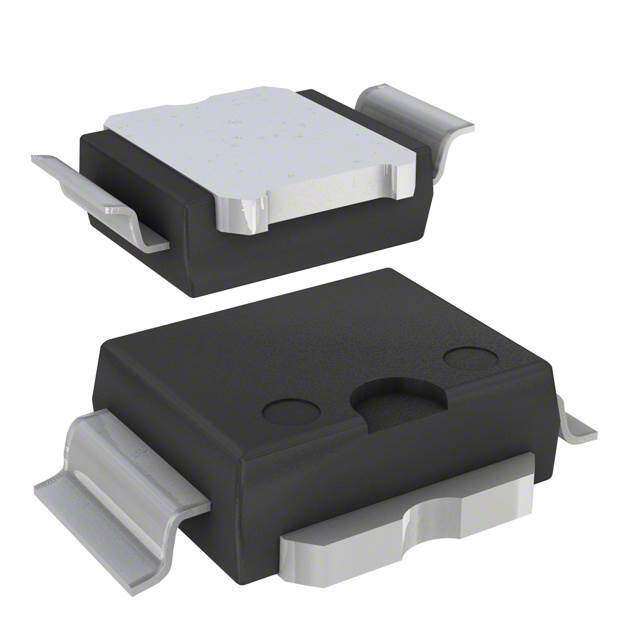
| 产品图片 |
|
| 产品型号 | CGH40025F |
| rohs | 无铅 / 符合限制有害物质指令(RoHS)规范要求 |
| 产品系列 | - |
| 产品目录页面 | |
| 供应商器件封装 | 440166 |
| 其它名称 | CGH40025FE |
| 功率-输出 | 30W |
| 包装 | 管件 |
| 噪声系数 | - |
| 增益 | 13dB |
| 封装/外壳 | 440166 |
| 晶体管类型 | HEMT |
| 标准包装 | 144 |
| 电压-测试 | 28V |
| 电压-额定 | 84V |
| 电流-测试 | 250mA |
| 配用 | /product-detail/zh/CGH40025F-TB/CGH40025F-TB-ND/1944144 |
| 频率 | 0Hz ~ 6GHz |
| 额定电流 | 7A |


- 商务部:美国ITC正式对集成电路等产品启动337调查
- 曝三星4nm工艺存在良率问题 高通将骁龙8 Gen1或转产台积电
- 太阳诱电将投资9.5亿元在常州建新厂生产MLCC 预计2023年完工
- 英特尔发布欧洲新工厂建设计划 深化IDM 2.0 战略
- 台积电先进制程称霸业界 有大客户加持明年业绩稳了
- 达到5530亿美元!SIA预计今年全球半导体销售额将创下新高
- 英特尔拟将自动驾驶子公司Mobileye上市 估值或超500亿美元
- 三星加码芯片和SET,合并消费电子和移动部门,撤换高东真等 CEO
- 三星电子宣布重大人事变动 还合并消费电子和移动部门
- 海关总署:前11个月进口集成电路产品价值2.52万亿元 增长14.8%


PDF Datasheet 数据手册内容提取
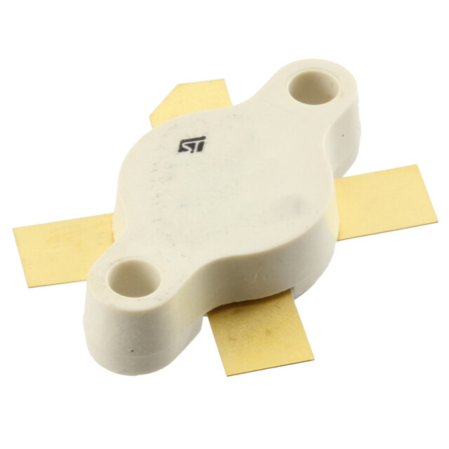
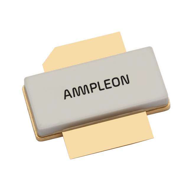
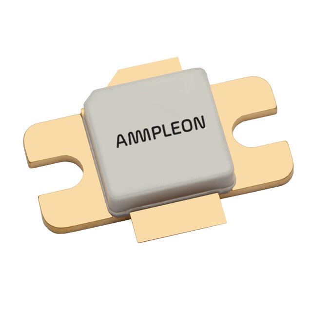
CGH40025 25 W, RF Power GaN HEMT Cree’s CGH40025 is an unmatched, gallium nitride (GaN) high electron mobility transistor (HEMT). The CGH40025, operating from a 28 volt rail, offers a general purpose, broadband solution to a variety of RF and microwave applications. GaN HEMTs offer high efficiency, high gain and wide bandwidth capabilities making the CGH40025 ideal for linear and compressed amplifier circuits. The transistor is available in a screw-down, flange package and solder-down, pill packages. PPacNk: aCgGeH T4y0p0e2: 454P0 a1n9d6 CaGndH 4404002156F6 FEATURES APPLICATIONS • Up to 6 GHz Operation • 2-Way Private Radio • 15 dB Small Signal Gain at 2.0 GHz • Broadband Amplifiers • 13 dB Small Signal Gain at 4.0 GHz • Cellular Infrastructure • 30 W typical P • Test Instrumentation SAT • 62 % Efficiency at P • Class A, AB, Linear amplifiers suitable for SAT • 28 V Operation OFDM, W-CDMA, EDGE, CDMA waveforms 5 1 0 2 y a M – 0 .4 v e R Subject to change without notice. 1 www.cree.com/wireless
Absolute Maximum Ratings (not simultaneous) at 25˚C Case Temperature Parameter Symbol Rating Units Conditions Drain-Source Voltage V 84 Volts 25˚C DSS Gate-to-Source Voltage V -10, +2 Volts 25˚C GS Storage Temperature T -65, +150 ˚C STG Operating Junction Temperature T 225 ˚C J Maximum Forward Gate Current I 7.0 mA 25˚C GMAX Maximum Drain Current1 I 3 A 25˚C DMAX Soldering Temperature2 T 245 ˚C S Screw Torque τ 60 in-oz Thermal Resistance, Junction to Case3 R 4.8 ˚C/W 85˚C θJC Case Operating Temperature3,4 T -40, +150 ˚C C Note: 1 Current limit for long term, reliable operation 2 Refer to the Application Note on soldering at www,wolfspeed.com/RF/Document-Library 3 Measured for the CGH40025F at P = 28 W. DISS 4 See also, the Power Dissipation De-rating Curve on Page 6. Electrical Characteristics (T = 25˚C) C Characteristics Symbol Min. Typ. Max. Units Conditions DC Characteristics1 Gate Threshold Voltage V -3.8 -3.0 -2.3 V V = 10 V, I = 7.2 mA GS(th) DC DS D Gate Quiescent Voltage V – -2.7 – V V = 28 V, I = 250 mA GS(Q) DC DS D Saturated Drain Current I 5.8 7.0 – A V = 6.0 V, V = 2.0 V DS DS GS Drain-Source Breakdown Voltage V 120 – – V V = -8 V, I = 7.2 mA BR DC GS D RF Characteristics2 (T = 25˚C, F = 3.7 GHz unless otherwise noted) C 0 Small Signal Gain G 12 13 – dB V = 28 V, I = 250 mA SS DD DQ Power Output3 P 20 30 – W V = 28 V, I = 250 mA SAT DD DQ Drain Efficiency4 η 55 62 – % V = 28 V, I = 250 mA, P DD DQ SAT No damage at all phase angles, Output Mismatch Stress VSWR – – 10 : 1 Y V = 28 V, I = 250 mA, DD DQ P = 25 W CW OUT Dynamic Characteristics Input Capacitance C – 9.0 – pF V = 28 V, V = -8 V, f = 1 MHz GS DS gs Output Capacitance C – 2.6 – pF V = 28 V, V = -8 V, f = 1 MHz DS DS gs Feedback Capacitance C – 0.4 – pF V = 28 V, V = -8 V, f = 1 MHz GD DS gs Notes: 1 Measured on wafer prior to packaging. 2 Measured in CGH40025-AMP. 3 P is defined as I = 0.72 mA. SAT G 4 Drain Efficiency = P / P OUT DC Cree, Inc. 4600 Silicon Drive Copyright © 2007-2015 Cree, Inc. All rights reserved. The information in this document is subject to change without notice. Cree and the Cree logo are Durham, North Carolina, USA 27703 registered trademarks of Cree, Inc. USA Tel: +1.919.313.5300 Fax: +1.919.869.2733 2 CGH40025 Rev 4.0 www.cree.com/rf
Typical Performance Small Signal Gain and Return Loss vs Frequency ofS tmhea lCl SGiHgn4a0l0 G2a5iFn iann tdh Ien pCuGtH R4e0tu0r2n5 L-AosMsP 20 15 10 5 B) d e ( 0 d u plit -5 m A -10 Small Signal Gain -15 Input Return Loss -20 -25 2.50 3.00 3.50 4.00 4.50 Frequency (GHz) P , Gain, and Drain Efficiency vs Frequency of the SAT Psat,CGGaiHn,4a0n0d2D5rFa iinn Ethffeic iCeGncHy4v0s0F2r5eq-AueMnPcyofthe CGH40025FintheCGH40025-TB V = 28 V, I = 250 mA VDDDD=28V,DIDQQ=250mA 40 80 Efficiency 35 70 30 60 B)B) %)%) (d(d 25 PSAT 50 y(y( nn cc aiai enen GG 20 40 cici W),W), EffiEffi (( nn PSAT15 30 DraiDrai Gain 10 20 Psat 5 Gain 10 DrainEff 0 0 3.40 3.45 3.50 3.55 3.60 3.65 3.70 3.75 3.80 Frequency(GHz) Cree, Inc. 4600 Silicon Drive Copyright © 2007-2015 Cree, Inc. All rights reserved. The information in this document is subject to change without notice. Cree and the Cree logo are Durham, North Carolina, USA 27703 registered trademarks of Cree, Inc. USA Tel: +1.919.313.5300 Fax: +1.919.869.2733 3 CGH40025 Rev 4.0 www.cree.com/rf
Typical Performance Swept CW Data of CGH40025 vs. Output Power with Source Swaepnt dC WLo Daadta Iomf CpGeHd4a0n02c5eFs v sO Oputtipmuti zPeowde fro wri tPh Sou Prcoe wanedr Liona dC IGmHpe4d0an0c2e5s -OApMtimPized for P3dB in CGH400S2A5TF-TB V = 28 V, I = 250 mA, Freq = 3.7 GHz DD Vdd = 28 VD,Q Idq = 250 mA, Freq = 3.7 GHz 15 70 14 60 13 50 %) y ( B)12 40 nc d e Gain (11 Gain (dB) 30 n Effici Drain Eff. (%) ai r D 10 20 9 10 8 0 20 25 30 35 40 45 Output Power (dBm) Maximum Available Gain and K Factor of the CGH40025 V = 28 V, I = 250 mA DD DQ ) B r d o G ( act A F M K Cree, Inc. 4600 Silicon Drive Copyright © 2007-2015 Cree, Inc. All rights reserved. The information in this document is subject to change without notice. Cree and the Cree logo are Durham, North Carolina, USA 27703 registered trademarks of Cree, Inc. USA Tel: +1.919.313.5300 Fax: +1.919.869.2733 4 CGH40025 Rev 4.0 www.cree.com/rf
Typical Noise Performance Simulated Minimum Noise Figure and Noise Resistance vs Frequency of the CGH40025F V = 28 V, I = 250 mA DD DQ ) B ) s d m ( e h r O u ( g e Fi c e an s t Noi sis m Re u e m s ni oi Mi N Electrostatic Discharge (ESD) Classifications Parameter Symbol Class Test Methodology Human Body Model HBM 1A > 250 V JEDEC JESD22 A114-D Charge Device Model CDM 1 < 200 V JEDEC JESD22 C101-C Cree, Inc. 4600 Silicon Drive Copyright © 2007-2015 Cree, Inc. All rights reserved. The information in this document is subject to change without notice. Cree and the Cree logo are Durham, North Carolina, USA 27703 registered trademarks of Cree, Inc. USA Tel: +1.919.313.5300 Fax: +1.919.869.2733 5 CGH40025 Rev 4.0 www.cree.com/rf
Source and Load Impedances D Z Source Z Load G S Frequency (MHz) Z Source Z Load 500 7.75 + j15.5 20 + j5.2 1000 3.11 + j5.72 17 + j6.66 1500 2.86 + j1.63 16.8 + j3.2 2500 2.4 - j3.52 8.02 + j4.32 3500 1.31 - j7.3 5.85 - j0.51 Note 1. V = 28V, I = 250mA in the 440166 package. DD DQ Note 2. Optimized for power gain, P and PAE. SAT Note 3. When using this device at low frequency, series resistors should be used to maintain amplifier stability. CGH40025 Power Dissipation De-rating Curve CGH40025FCWPowerDissipationDe-ratingCurve 30 25 W)W) (( nn atioatio 20 pp sisi ss DiDi erer 15 ww oo Note1 PP 10 5 0 0 25 50 75 100 125 150 175 200 225 250 MaximumCaseTemperature(°C) Note 1. Area exceeds Maximum Case Operating Temperature (See Page 2). Cree, Inc. 4600 Silicon Drive Copyright © 2007-2015 Cree, Inc. All rights reserved. The information in this document is subject to change without notice. Cree and the Cree logo are Durham, North Carolina, USA 27703 registered trademarks of Cree, Inc. USA Tel: +1.919.313.5300 Fax: +1.919.869.2733 6 CGH40025 Rev 4.0 www.cree.com/rf
CGH40025-AMP Demonstration Amplifier Circuit Schematic CGH40025-AMP Demonstration Amplifier Circuit Outline Cree, Inc. 4600 Silicon Drive Copyright © 2007-2015 Cree, Inc. All rights reserved. The information in this document is subject to change without notice. Cree and the Cree logo are Durham, North Carolina, USA 27703 registered trademarks of Cree, Inc. USA Tel: +1.919.313.5300 Fax: +1.919.869.2733 7 CGH40025 Rev 4.0 www.cree.com/rf
CGH40025-AMP Demonstration Amplifier Circuit Bill of Materials Designator Description Qty R2 RES,1/16W,0603,1%,47 OHMS 1 R1 RES,1/16W,0603,1%,100 OHMS 1 C6 CAP, 470PF, 5%,100V, 0603 1 C16 CAP, 33 UF, 20%, G CASE 1 C15 CAP, 1.0UF, 100V, 10%, X7R, 1210 1 C8 CAP 10UF 16V TANTALUM 1 C13 CAP, 100.0pF, +/-5%, 0603 1 C1 CAP, 0.8pF, +/-0.1pF, 0603 1 C2 CAP, 0.5pF, +/-0.05pF, 0603 1 C9,C10 CAP, 1.0pF, +/-0.1pF, 0603 2 C4,C11 CAP, 10.0pF,+/-5%, 0603 2 C5,C12 CAP, 39pF, +/-5%, 0603 2 C7,C14 CAP,33000PF, 0805,100V, X7R 2 J3,J4 CONN SMA STR PANEL JACK RECP 2 J1 HEADER RT>PLZ .1CEN LK 5POS 1 - PCB, RO4350B, Er = 3.48, h = 20 mil 1 - CGH40025F or CGH40025P 1 CGH40025F-AMP Demonstration Amplifier Circuit Cree, Inc. 4600 Silicon Drive Copyright © 2007-2015 Cree, Inc. All rights reserved. The information in this document is subject to change without notice. Cree and the Cree logo are Durham, North Carolina, USA 27703 registered trademarks of Cree, Inc. USA Tel: +1.919.313.5300 Fax: +1.919.869.2733 8 CGH40025 Rev 4.0 www.cree.com/rf
Typical Package S-Parameters for CGH40025 (Small Signal, V = 28 V, I = 100 mA, angle in degrees) DS DQ Frequency Mag S11 Ang S11 Mag S21 Ang S21 Mag S12 Ang S12 Mag S22 Ang S22 500 MHz 0.902 -151.72 11.80 92.09 0.025 6.22 0.393 -140.34 600 MHz 0.901 -157.13 9.89 87.31 0.025 2.28 0.402 -143.54 700 MHz 0.900 -161.20 8.49 83.18 0.025 -0.99 0.412 -145.64 800 MHz 0.900 -164.41 7.42 79.49 0.025 -3.82 0.424 -147.11 900 MHz 0.901 -167.04 6.58 76.10 0.024 -6.33 0.436 -148.22 1.0 GHz 0.902 -169.26 5.89 72.93 0.024 -8.60 0.449 -149.12 1.1 GHz 0.903 -171.19 5.33 69.93 0.024 -10.69 0.462 -149.91 1.2 GHz 0.904 -172.89 4.86 67.07 0.023 -12.61 0.476 -150.65 1.3 GHz 0.905 -174.43 4.45 64.33 0.023 -14.39 0.489 -151.38 1.4 GHz 0.906 -175.84 4.10 61.68 0.022 -16.06 0.503 -152.12 1.5 GHz 0.907 -177.14 3.80 59.12 0.022 -17.61 0.517 -152.87 1.6 GHz 0.909 -178.36 3.54 56.64 0.022 -19.05 0.531 -153.65 1.7 GHz 0.910 -179.52 3.30 54.22 0.021 -20.38 0.545 -154.46 1.8 GHz 0.912 179.38 3.09 51.87 0.021 -21.62 0.558 -155.29 1.9 GHz 0.913 178.33 2.90 49.58 0.020 -22.75 0.571 -156.15 2.0 GHz 0.914 177.30 2.73 47.34 0.020 -23.78 0.584 -157.04 2.1 GHz 0.916 176.31 2.58 45.15 0.019 -24.70 0.596 -157.95 2.2 GHz 0.917 175.34 2.44 43.02 0.019 -25.52 0.608 -158.88 2.3 GHz 0.918 174.39 2.31 40.92 0.018 -26.22 0.620 -159.82 2.4 GHz 0.920 173.46 2.19 38.88 0.018 -26.82 0.631 -160.78 2.5 GHz 0.921 172.54 2.09 36.87 0.017 -27.29 0.642 -161.76 2.6 GHz 0.922 171.63 1.99 34.91 0.016 -27.64 0.652 -162.74 2.7 GHz 0.923 170.73 1.90 32.98 0.016 -27.85 0.662 -163.73 2.8 GHz 0.925 169.84 1.82 31.09 0.015 -27.92 0.672 -164.73 2.9 GHz 0.926 168.95 1.74 29.24 0.015 -27.85 0.681 -165.73 3.0 GHz 0.927 168.07 1.67 27.41 0.014 -27.61 0.690 -166.74 3.2 GHz 0.929 166.30 1.54 23.86 0.013 -26.63 0.706 -168.76 3.4 GHz 0.931 164.54 1.42 20.42 0.013 -24.89 0.721 -170.79 3.6 GHz 0.932 162.78 1.33 17.08 0.012 -22.30 0.735 -172.82 3.8 GHz 0.934 161.00 1.24 13.84 0.011 -18.80 0.748 -174.85 4.0 GHz 0.935 159.21 1.16 10.67 0.011 -14.40 0.759 -176.88 4.2 GHz 0.936 157.39 1.10 7.58 0.010 -9.18 0.769 -178.90 4.4 GHz 0.937 155.55 1.04 4.55 0.010 -3.38 0.778 179.07 4.6 GHz 0.938 153.67 0.98 1.57 0.010 2.65 0.787 177.04 4.8 GHz 0.939 151.77 0.94 -1.36 0.011 8.52 0.794 175.00 5.0 GHz 0.939 149.82 0.89 -4.25 0.011 13.87 0.801 172.96 5.2 GHz 0.939 147.82 0.86 -7.11 0.012 18.48 0.807 170.90 5.4 GHz 0.939 145.78 0.82 -9.95 0.013 22.25 0.812 168.83 5.6 GHz 0.940 143.68 0.79 -12.78 0.014 25.17 0.817 166.74 5.8 GHz 0.939 141.53 0.77 -15.59 0.016 27.32 0.821 164.62 6.0 GHz 0.939 139.31 0.74 -18.41 0.017 28.77 0.825 162.48 To download the s-parameters in s2p format, go to the CGH40025 Product Page and click on the documentation tab. Cree, Inc. 4600 Silicon Drive Copyright © 2007-2015 Cree, Inc. All rights reserved. The information in this document is subject to change without notice. Cree and the Cree logo are Durham, North Carolina, USA 27703 registered trademarks of Cree, Inc. USA Tel: +1.919.313.5300 Fax: +1.919.869.2733 9 CGH40025 Rev 4.0 www.cree.com/rf
Typical Package S-Parameters for CGH40025 (Small Signal, V = 28 V, I = 250 mA, angle in degrees) DS DQ Frequency Mag S11 Ang S11 Mag S21 Ang S21 Mag S12 Ang S12 Mag S22 Ang S22 500 MHz 0.917 -157.22 12.62 91.45 0.018 7.56 0.458 -158.97 600 MHz 0.916 -161.92 10.57 87.33 0.018 4.70 0.465 -160.93 700 MHz 0.916 -165.46 9.07 83.78 0.018 2.41 0.472 -162.19 800 MHz 0.916 -168.28 7.94 80.58 0.018 0.51 0.478 -163.04 900 MHz 0.916 -170.61 7.05 77.64 0.017 -1.12 0.485 -163.64 1.0 GHz 0.916 -172.60 6.33 74.88 0.017 -2.55 0.493 -164.09 1.1 GHz 0.917 -174.33 5.74 72.25 0.017 -3.82 0.500 -164.45 1.2 GHz 0.917 -175.88 5.24 69.73 0.017 -4.94 0.508 -164.77 1.3 GHz 0.918 -177.28 4.82 67.30 0.017 -5.95 0.516 -165.06 1.4 GHz 0.918 -178.57 4.46 64.94 0.017 -6.84 0.525 -165.36 1.5 GHz 0.919 -179.78 4.14 62.65 0.016 -7.63 0.533 -165.67 1.6 GHz 0.919 179.09 3.87 60.41 0.016 -8.31 0.542 -165.99 1.7 GHz 0.920 178.01 3.62 58.22 0.016 -8.90 0.550 -166.35 1.8 GHz 0.921 176.98 3.40 56.07 0.016 -9.39 0.559 -166.73 1.9 GHz 0.921 175.99 3.21 53.97 0.015 -9.77 0.568 -167.14 2.0 GHz 0.922 175.03 3.03 51.90 0.015 -10.06 0.577 -167.59 2.1 GHz 0.923 174.09 2.87 49.87 0.015 -10.24 0.585 -168.07 2.2 GHz 0.924 173.17 2.73 47.87 0.014 -10.31 0.594 -168.57 2.3 GHz 0.924 172.27 2.60 45.91 0.014 -10.27 0.602 -169.11 2.4 GHz 0.925 171.39 2.47 43.97 0.014 -10.12 0.610 -169.67 2.5 GHz 0.926 170.51 2.36 42.07 0.014 -9.85 0.619 -170.26 2.6 GHz 0.926 169.65 2.26 40.19 0.013 -9.46 0.626 -170.88 2.7 GHz 0.927 168.79 2.16 38.34 0.013 -8.95 0.634 -171.52 2.8 GHz 0.928 167.93 2.08 36.52 0.013 -8.31 0.642 -172.17 2.9 GHz 0.928 167.08 1.99 34.72 0.013 -7.54 0.649 -172.85 3.0 GHz 0.929 166.24 1.92 32.94 0.013 -6.65 0.656 -173.55 3.2 GHz 0.930 164.54 1.78 29.45 0.012 -4.49 0.670 -175.00 3.4 GHz 0.931 162.85 1.66 26.05 0.012 -1.85 0.683 -176.50 3.6 GHz 0.932 161.14 1.55 22.72 0.012 1.19 0.695 -178.06 3.8 GHz 0.933 159.42 1.46 19.46 0.012 4.55 0.706 -179.66 4.0 GHz 0.933 157.68 1.38 16.27 0.012 8.08 0.716 178.70 4.2 GHz 0.934 155.91 1.31 13.12 0.012 11.64 0.726 177.02 4.4 GHz 0.934 154.11 1.24 10.03 0.013 15.08 0.735 175.30 4.6 GHz 0.935 152.28 1.18 6.97 0.013 18.26 0.743 173.56 4.8 GHz 0.935 150.41 1.13 3.95 0.014 21.09 0.750 171.78 5.0 GHz 0.935 148.49 1.08 0.96 0.015 23.50 0.756 169.97 5.2 GHz 0.935 146.53 1.04 -2.00 0.016 25.48 0.762 168.12 5.4 GHz 0.935 144.52 1.00 -4.96 0.017 27.02 0.768 166.24 5.6 GHz 0.935 142.45 0.97 -7.90 0.018 28.12 0.773 164.32 5.8 GHz 0.934 140.31 0.94 -10.84 0.020 28.83 0.777 162.36 6.0 GHz 0.934 138.12 0.91 -13.79 0.021 29.18 0.781 160.36 To download the s-parameters in s2p format, go to the CGH40025 Product Page and click on the documentation tab. Cree, Inc. 4600 Silicon Drive Copyright © 2007-2015 Cree, Inc. All rights reserved. The information in this document is subject to change without notice. Cree and the Cree logo are Durham, North Carolina, USA 27703 registered trademarks of Cree, Inc. USA Tel: +1.919.313.5300 Fax: +1.919.869.2733 10 CGH40025 Rev 4.0 www.cree.com/rf
Typical Package S-Parameters for CGH40025 (Small Signal, V = 28 V, I = 400 mA, angle in degrees) DS DQ Frequency Mag S11 Ang S11 Mag S21 Ang S21 Mag S12 Ang S12 Mag S22 Ang S22 500 MHz 0.924 -159.12 12.64 91.13 0.015 8.27 0.485 -163.72 600 MHz 0.923 -163.56 10.58 87.23 0.015 5.84 0.491 -165.34 700 MHz 0.923 -166.92 9.08 83.86 0.015 3.96 0.497 -166.41 800 MHz 0.923 -169.60 7.95 80.83 0.015 2.43 0.502 -167.13 900 MHz 0.923 -171.82 7.06 78.03 0.015 1.16 0.508 -167.65 1.0 GHz 0.923 -173.72 6.34 75.40 0.015 0.08 0.514 -168.05 1.1 GHz 0.923 -175.39 5.75 72.89 0.015 -0.84 0.520 -168.36 1.2 GHz 0.924 -176.88 5.26 70.48 0.015 -1.62 0.526 -168.63 1.3 GHz 0.924 -178.24 4.84 68.15 0.015 -2.29 0.533 -168.88 1.4 GHz 0.924 -179.50 4.48 65.89 0.015 -2.85 0.539 -169.13 1.5 GHz 0.925 179.33 4.17 63.68 0.014 -3.31 0.546 -169.38 1.6 GHz 0.925 178.22 3.89 61.52 0.014 -3.67 0.553 -169.65 1.7 GHz 0.926 177.17 3.65 59.41 0.014 -3.93 0.560 -169.94 1.8 GHz 0.926 176.16 3.43 57.34 0.014 -4.09 0.568 -170.26 1.9 GHz 0.927 175.18 3.24 55.30 0.014 -4.16 0.575 -170.60 2.0 GHz 0.927 174.24 3.07 53.29 0.014 -4.13 0.582 -170.97 2.1 GHz 0.928 173.32 2.91 51.32 0.013 -4.00 0.589 -171.36 2.2 GHz 0.928 172.41 2.76 49.38 0.013 -3.76 0.597 -171.79 2.3 GHz 0.929 171.53 2.63 47.46 0.013 -3.43 0.604 -172.24 2.4 GHz 0.929 170.65 2.51 45.57 0.013 -2.99 0.611 -172.71 2.5 GHz 0.929 169.79 2.40 43.71 0.013 -2.44 0.618 -173.22 2.6 GHz 0.930 168.93 2.30 41.87 0.013 -1.79 0.625 -173.75 2.7 GHz 0.930 168.08 2.20 40.05 0.012 -1.04 0.632 -174.30 2.8 GHz 0.931 167.24 2.12 38.26 0.012 -0.18 0.638 -174.87 2.9 GHz 0.931 166.40 2.04 36.48 0.012 0.77 0.645 -175.47 3.0 GHz 0.932 165.56 1.96 34.73 0.012 1.82 0.651 -176.08 3.2 GHz 0.932 163.88 1.82 31.28 0.012 4.18 0.663 -177.37 3.4 GHz 0.933 162.20 1.70 27.91 0.012 6.83 0.675 -178.72 3.6 GHz 0.934 160.51 1.60 24.60 0.012 9.69 0.686 179.86 3.8 GHz 0.934 158.80 1.51 21.35 0.012 12.64 0.696 178.39 4.0 GHz 0.935 157.07 1.42 18.16 0.013 15.58 0.706 176.88 4.2 GHz 0.935 155.32 1.35 15.01 0.013 18.40 0.715 175.31 4.4 GHz 0.935 153.53 1.29 11.91 0.014 21.01 0.723 173.70 4.6 GHz 0.935 151.70 1.23 8.84 0.014 23.33 0.730 172.05 4.8 GHz 0.935 149.84 1.17 5.80 0.015 25.32 0.737 170.36 5.0 GHz 0.935 147.93 1.13 2.79 0.016 26.96 0.743 168.63 5.2 GHz 0.935 145.98 1.09 -0.20 0.017 28.24 0.749 166.86 5.4 GHz 0.935 143.97 1.05 -3.19 0.018 29.16 0.754 165.05 5.6 GHz 0.934 141.91 1.01 -6.16 0.020 29.75 0.759 163.20 5.8 GHz 0.934 139.78 0.98 -9.14 0.021 30.02 0.763 161.30 6.0 GHz 0.933 137.58 0.96 -12.12 0.023 29.99 0.767 159.35 To download the s-parameters in s2p format, go to the CGH40025 Product Page and click on the documentation tab. Cree, Inc. 4600 Silicon Drive Copyright © 2007-2015 Cree, Inc. All rights reserved. The information in this document is subject to change without notice. Cree and the Cree logo are Durham, North Carolina, USA 27703 registered trademarks of Cree, Inc. USA Tel: +1.919.313.5300 Fax: +1.919.869.2733 11 CGH40025 Rev 4.0 www.cree.com/rf
Product Dimensions CGH40025F (Package Type — 440166) Product Dimensions CGH40025P (Package Type — 440196) Cree, Inc. 4600 Silicon Drive Copyright © 2007-2015 Cree, Inc. All rights reserved. The information in this document is subject to change without notice. Cree and the Cree logo are Durham, North Carolina, USA 27703 registered trademarks of Cree, Inc. USA Tel: +1.919.313.5300 Fax: +1.919.869.2733 12 CGH40025 Rev 4.0 www.cree.com/rf
Product Ordering Information Order Number Description Unit of Measure Image CGH40025F GaN HEMT Each CGH40025P GaN HEMT Each CGH40025F-TB Test board without GaN HEMT Each CGH40025F-AMP Test board with GaN HEMT installed Each Cree, Inc. 4600 Silicon Drive Copyright © 2007-2015 Cree, Inc. All rights reserved. The information in this document is subject to change without notice. Cree and the Cree logo are Durham, North Carolina, USA 27703 registered trademarks of Cree, Inc. USA Tel: +1.919.313.5300 Fax: +1.919.869.2733 13 CGH40025 Rev 4.0 www.cree.com/rf
Disclaimer Specifications are subject to change without notice. Cree, Inc. believes the information contained within this data sheet to be accurate and reliable. However, no responsibility is assumed by Cree for any infringement of patents or other rights of third parties which may result from its use. No license is granted by implication or otherwise under any patent or patent rights of Cree. Cree makes no warranty, representation or guarantee regarding the suitability of its products for any particular purpose. “Typical” parameters are the average values expected by Cree in large quantities and are provided for information purposes only. These values can and do vary in different applications and actual performance can vary over time. All operating parameters should be validated by customer’s technical experts for each application. Cree products are not designed, intended or authorized for use as components in applications intended for surgical implant into the body or to support or sustain life, in applications in which the failure of the Cree product could result in personal injury or death or in applications for planning, construction, maintenance or direct operation of a nuclear facility. For more information, please contact: Cree, Inc. 4600 Silicon Drive Durham, North Carolina, USA 27703 www.cree.com/RF Sarah Miller Marketing & Export Cree, RF Components 1.919.407.5302 Ryan Baker Marketing Cree, RF Components 1.919.407.7816 Tom Dekker Sales Director Cree, RF Components 1.919.407.5639 Cree, Inc. 4600 Silicon Drive Copyright © 2007-2015 Cree, Inc. All rights reserved. The information in this document is subject to change without notice. Cree and the Cree logo are Durham, North Carolina, USA 27703 registered trademarks of Cree, Inc. USA Tel: +1.919.313.5300 Fax: +1.919.869.2733 14 CGH40025 Rev 4.0 www.cree.com/rf
Mouser Electronics Authorized Distributor Click to View Pricing, Inventory, Delivery & Lifecycle Information: C ree, Inc.: CGH40025F CGH40025F-TB