ICGOO在线商城 > 分立半导体产品 > 晶体管 - FET,MOSFET - 单 > BUK9Y4R8-60E,115
 Datasheet下载
- 型号: BUK9Y4R8-60E,115
- 制造商: NXP Semiconductors
- 库位|库存: xxxx|xxxx
- 要求:
| 数量阶梯 | 香港交货 | 国内含税 |
| +xxxx | $xxxx | ¥xxxx |
查看当月历史价格
查看今年历史价格
BUK9Y4R8-60E,115产品简介:
ICGOO电子元器件商城为您提供BUK9Y4R8-60E,115由NXP Semiconductors设计生产,在icgoo商城现货销售,并且可以通过原厂、代理商等渠道进行代购。 BUK9Y4R8-60E,115价格参考。NXP SemiconductorsBUK9Y4R8-60E,115封装/规格:晶体管 - FET,MOSFET - 单, 表面贴装 N 沟道 60V 100A(Tc) 238W(Tc) LFPAK56,Power-SO8。您可以下载BUK9Y4R8-60E,115参考资料、Datasheet数据手册功能说明书,资料中有BUK9Y4R8-60E,115 详细功能的应用电路图电压和使用方法及教程。
Nexperia USA Inc. 生产的 BUK9Y4R8-60E,115 是一款单通道 MOSFET(金属氧化物场效应晶体管),具体应用场景如下:

 1. 电源管理
   该型号的 MOSFET 主要用于电源管理电路中,如开关电源(SMPS)、DC-DC 转换器、AC-DC 适配器等。其低导通电阻(Rds(on))特性使得它在高效能电源转换应用中表现出色,能够减少功率损耗,提高整体效率。

 2. 电机驱动
   在电机驱动应用中,BUK9Y4R8-60E,115 可以用于控制电机的启动、停止和调速。MOSFET 的快速开关特性和低导通电阻有助于实现高效的电机控制,同时减少发热和能量损失。

 3. 电池管理系统 (BMS)
   在电池管理系统中,该 MOSFET 可用于电池充放电保护电路,确保电池在安全范围内工作。它可以在过流、过压或短路等异常情况下迅速切断电流路径,保护电池和相关电路免受损坏。

 4. 工业自动化
   在工业自动化设备中,BUK9Y4R8-60E,115 可用于各种开关控制电路,如继电器替代、电磁阀驱动等。其高可靠性和长寿命使其成为工业环境中理想的开关元件。

 5. 消费电子
   在消费电子产品中,如智能手机、平板电脑、笔记本电脑等,该 MOSFET 可用于负载开关、充电电路等。其小型封装和低功耗特性使其非常适合便携式设备中的应用。

 6. 汽车电子
   在汽车电子系统中,BUK9Y4R8-60E,115 可用于车身控制系统、车载充电器、电动助力转向系统(EPS)等。其耐高温和抗干扰能力强,能够在恶劣的汽车环境中稳定工作。

 总结
BUK9Y4R8-60E,115 具有低导通电阻、快速开关速度和高可靠性等特点,适用于多种应用场景,尤其是在需要高效能、低功耗和高可靠性的电源管理和控制电路中表现尤为突出。
| 参数 | 数值 |
| 产品目录 | |
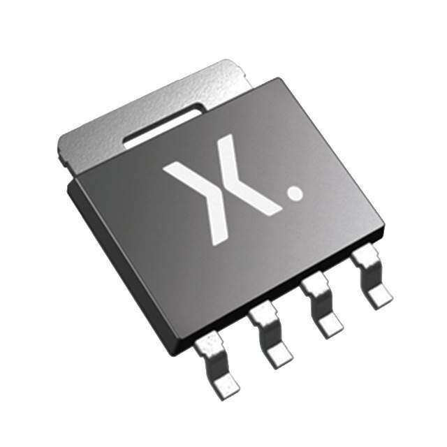
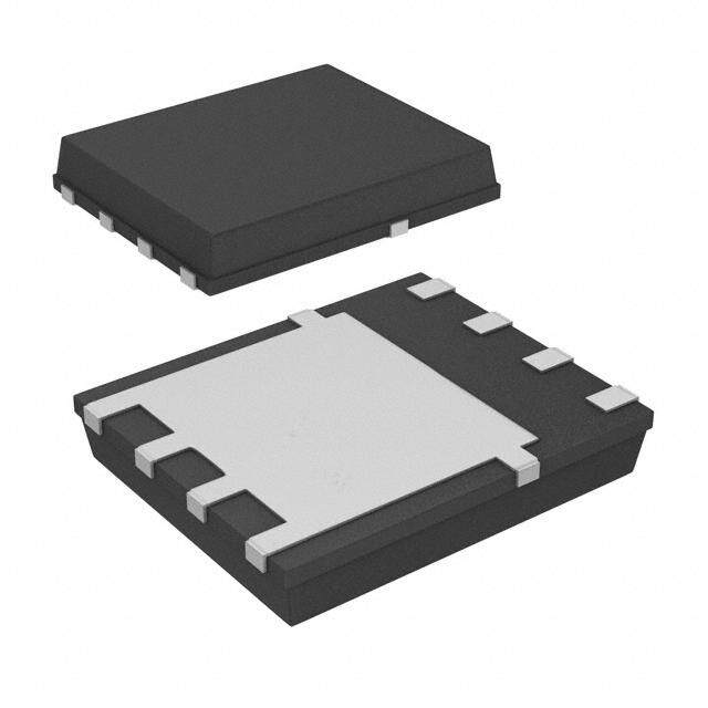
| 描述 | MOSFET N-CH 60V LFPAK |
| 产品分类 | FET - 单 |
| FET功能 | 逻辑电平门 |
| FET类型 | MOSFET N 通道,金属氧化物 |
| 品牌 | NXP Semiconductors |
| 数据手册 | |
| 产品图片 |
|
| 产品型号 | BUK9Y4R8-60E,115 |
| rohs | 无铅 / 符合限制有害物质指令(RoHS)规范要求 |
| 产品系列 | TrenchMOS™ |
| 不同Id时的Vgs(th)(最大值) | 2.1V @ 1mA |
| 不同Vds时的输入电容(Ciss) | 7853pF @ 25V |
| 不同Vgs时的栅极电荷(Qg) | 50nC @ 5V |
| 不同 Id、Vgs时的 RdsOn(最大值) | 4.1 毫欧 @ 25A,10V |
| 供应商器件封装 | LFPAK56, Power-SO8 |
| 其它名称 | 568-10983-2 |
| 功率-最大值 | 238W |
| 包装 | 带卷 (TR) |
| 安装类型 | 表面贴装 |
| 封装/外壳 | SC-100,SOT-669,4-LFPAK |
| 标准包装 | 1,500 |
| 漏源极电压(Vdss) | 60V |
| 电流-连续漏极(Id)(25°C时) | 100A (Ta) |


- 商务部:美国ITC正式对集成电路等产品启动337调查
- 曝三星4nm工艺存在良率问题 高通将骁龙8 Gen1或转产台积电
- 太阳诱电将投资9.5亿元在常州建新厂生产MLCC 预计2023年完工
- 英特尔发布欧洲新工厂建设计划 深化IDM 2.0 战略
- 台积电先进制程称霸业界 有大客户加持明年业绩稳了
- 达到5530亿美元!SIA预计今年全球半导体销售额将创下新高
- 英特尔拟将自动驾驶子公司Mobileye上市 估值或超500亿美元
- 三星加码芯片和SET,合并消费电子和移动部门,撤换高东真等 CEO
- 三星电子宣布重大人事变动 还合并消费电子和移动部门
- 海关总署:前11个月进口集成电路产品价值2.52万亿元 增长14.8%


PDF Datasheet 数据手册内容提取
BUK9Y4R8-60E N-channel 60 V, 4.8 mΩ logic level MOSFET in LFPAK56 7 January 2016 Product data sheet 1. General description Logic level N-channel MOSFET in an LFPAK56 (Power SO8) package using TrenchMOS technology. This product has been designed and qualified to AEC Q101 standard for use in high performance automotive applications. 2. Features and benefits • Q101 compliant • Repetitive avalanche rated • Suitable for thermally demanding environments due to 175 °C rating • True logic level gate with V rating of greater than 0.5 V at 175 °C GS(th) 3. Applications • 12 V Automotive systems • Motors, lamps and solenoid control • Transmission control • Ultra high performance power switching 4. Quick reference data Table 1. Quick reference data Symbol Parameter Conditions Min Typ Max Unit V drain-source voltage 25 °C ≤ T ≤ 175 °C - - 60 V DS j ID drain current VGS = 5 V; Tmb = 25 °C; Fig. 2 [1] - - 100 A P total power dissipation T = 25 °C; Fig. 1 - - 238 W tot mb Static characteristics R drain-source on-state V = 5 V; I = 25 A; T = 25 °C; Fig. 11 - 3.3 4.8 mΩ DSon GS D j resistance Dynamic characteristics Q gate-drain charge I = 25 A; V = 48 V; V = 5 V; - 18.1 - nC GD D DS GS T = 25 °C; Fig. 13; Fig. 14 j [1] Continuous current is limited by package.
Nexperia BUK9Y4R8-60E N-channel 60 V, 4.8 mΩ logic level MOSFET in LFPAK56 5. Pinning information Table 2. Pinning information Pin Symbol Description Simplified outline Graphic symbol 1 S source mb D 2 S source G 3 S source 4 G gate mbb076 S 1 2 3 4 mb D mounting base; connected to LFPAK56; Power- drain SO8 (SOT669) 6. Ordering information Table 3. Ordering information Type number Package Name Description Version BUK9Y4R8-60E LFPAK56; Plastic single-ended surface-mounted package SOT669 Power-SO8 (LFPAK56; Power-SO8); 4 leads 7. Marking Table 4. Marking codes Type number Marking code BUK9Y4R8-60E 94E860 8. Limiting values Table 5. Limiting values In accordance with the Absolute Maximum Rating System (IEC 60134). Symbol Parameter Conditions Min Max Unit V drain-source voltage 25 °C ≤ T ≤ 175 °C - 60 V DS j V drain-gate voltage R = 20 kΩ - 60 V DGR GS V gate-source voltage DC; T ≤ 175 °C -10 10 V GS j Pulsed; Tj ≤ 175 °C [1][2] -15 15 V P total power dissipation T = 25 °C; Fig. 1 - 238 W tot mb ID drain current VGS = 5 V; Tmb = 25 °C; Fig. 2 [3] - 100 A VGS = 5 V; Tmb = 100 °C; Fig. 2 [3] - 100 A I peak drain current pulsed; t ≤ 10 µs; T = 25 °C; Fig. 3 - 593 A DM p mb BUK9Y4R8-60E All information provided in this document is subject to legal disclaimers. © Nexperia B.V. 2017. All rights reserved Product data sheet 7 January 2016 2 / 13
Nexperia BUK9Y4R8-60E N-channel 60 V, 4.8 mΩ logic level MOSFET in LFPAK56 Symbol Parameter Conditions Min Max Unit T storage temperature -55 175 °C stg T junction temperature -55 175 °C j Source-drain diode IS source current Tmb = 25 °C [3] - 100 A I peak source current pulsed; t ≤ 10 µs; T = 25 °C - 593 A SM p mb Avalanche ruggedness EDS(AL)S non-repetitive drain-source ID = 100 A; Vsup ≤ 60 V; RGS = 50 Ω; [4][5] - 199 mJ avalanche energy V = 5 V; T = 25 °C; unclamped; GS j(init) Fig. 4 [1] Accumulated pulse duration up to 50 hours delivers zero defect ppm [2] Significantly longer life times are achieved by lowering Tj and or VGS [3] Continuous current is limited by package. [4] Single-pulse avalanche rating limited by maximum junction temperature of 175 °C. [5] Refer to application note AN10273 for further information. 03aa16 003aaj140 120 200 ID Pder (A) (%) 150 80 100 (1) 40 50 0 0 0 50 100 150 200 0 50 100 150 200 Tmb(°C) Tmb(°C) (1) Capped at 100A due to package Fig. 1. Normalized total power dissipation as a function of mounting base temperature Fig. 2. Continuous drain current as a function of mounting base temperature BUK9Y4R8-60E All information provided in this document is subject to legal disclaimers. © Nexperia B.V. 2017. All rights reserved Product data sheet 7 January 2016 3 / 13
Nexperia BUK9Y4R8-60E N-channel 60 V, 4.8 mΩ logic level MOSFET in LFPAK56 103 003aaj142 ID LimitRDSon=VDS/ID (A) tp=10µs 102 100µs 10 1ms DC 10ms 1 100ms 10-1 10-1 1 10 102 103 VDS(V) Fig. 3. Safe operating area; continuous and peak drain currents as a function of drain-source voltage 103 003aaj141 IAL (A) 102 (1) 10 (2) 1 (3) 10-1 10-3 10-2 10-1 1 10 tAL(ms) Fig. 4. Avalanche rating; avalanche current as a function of avalanche time 9. Thermal characteristics Table 6. Thermal characteristics Symbol Parameter Conditions Min Typ Max Unit R thermal resistance Fig. 5 - - 0.63 K/W th(j-mb) from junction to mounting base BUK9Y4R8-60E All information provided in this document is subject to legal disclaimers. © Nexperia B.V. 2017. All rights reserved Product data sheet 7 January 2016 4 / 13
Nexperia BUK9Y4R8-60E N-channel 60 V, 4.8 mΩ logic level MOSFET in LFPAK56 003aai463 1 ZZtthh((jj--mmbb)) ((KK//WW)) δδ == 00..55 00..22 10-1 00..11 00..0055 00..0022 10-2 ssiinnggllee sshhoott P δ = tp T tp t T 10-3 10-6 10-5 10-4 10-3 10-2 10-1 1 tp (s) Fig. 5. Transient thermal impedance from junction to mounting base as a function of pulse duration 10. Characteristics Table 7. Characteristics Symbol Parameter Conditions Min Typ Max Unit Static characteristics V drain-source I = 250 µA; V = 0 V; T = 25 °C 60 - - V (BR)DSS D GS j breakdown voltage I = 250 µA; V = 0 V; T = -55 °C 54 - - V D GS j V gate-source threshold I = 1 mA; V =V ; T = 25 °C; Fig. 9; 1.4 1.7 2.1 V GS(th) D DS GS j voltage Fig. 10 I = 1 mA; V =V ; T = -55 °C; Fig. 9 - - 2.45 V D DS GS j I = 1 mA; V =V ; T = 175 °C; Fig. 9 0.5 - - V D DS GS j I drain leakage current V = 60 V; V = 0 V; T = 25 °C - 0.12 10 µA DSS DS GS j V = 60 V; V = 0 V; T = 175 °C - - 500 µA DS GS j I gate leakage current V = 10 V; V = 0 V; T = 25 °C - 2 100 nA GSS GS DS j V = -10 V; V = 0 V; T = 25 °C - 2 100 nA GS DS j R drain-source on-state V = 5 V; I = 25 A; T = 25 °C; Fig. 11 - 3.3 4.8 mΩ DSon GS D j resistance V = 10 V; I = 25 A; T = 25 °C; - 2.9 4.1 mΩ GS D j Fig. 11 V = 5 V; I = 25 A; T = 175 °C; - - 10.8 mΩ GS D j Fig. 11; Fig. 12 Dynamic characteristics Q total gate charge I = 25 A; V = 48 V; V = 5 V; - 54.8 - nC G(tot) D DS GS T = 25 °C; Fig. 13; Fig. 14 Q gate-source charge j - 13.6 - nC GS Q gate-drain charge - 18.1 - nC GD BUK9Y4R8-60E All information provided in this document is subject to legal disclaimers. © Nexperia B.V. 2017. All rights reserved Product data sheet 7 January 2016 5 / 13
Nexperia BUK9Y4R8-60E N-channel 60 V, 4.8 mΩ logic level MOSFET in LFPAK56 Symbol Parameter Conditions Min Typ Max Unit C input capacitance V = 25 V; V = 0 V; f = 1 MHz; - 5890 7853 pF iss DS GS T = 25 °C; Fig. 15 C output capacitance j - 506 607 pF oss C reverse transfer - 276 378 pF rss capacitance t turn-on delay time V = 45 V; R = 1.8 Ω; V = 5 V; - 28 - ns d(on) DS L GS R = 5 Ω; T = 25 °C t rise time G(ext) j - 53 - ns r t turn-off delay time - 80 - ns d(off) t fall time - 47 - ns f Source-drain diode V source-drain voltage I = 25 A; V = 0 V; T = 25 °C; Fig. 16 - 0.78 1.2 V SD S GS j t reverse recovery time I = 20 A; dI /dt = -100 A/µs; V = 0 V; - 29 - ns rr S S GS V = 25 V; T = 25 °C Q recovered charge DS j - 28 - nC r 003aaj144 003aaj145 360 10 R ID VGS(V)=10 4.5 (mDΩSo)n (A) 3.5 7.5 240 5 3 120 2.5 2.8 2.6 2.4 0 0 0 2 V (V) 4 0 2.5 5 7.5 V (V)10 DS GS T = 25 °C; t = 300 μs j p Fig. 7. Drain-source on-state resistance as a function Fig. 6. Output characteristics; drain current as a of gate-source voltage; typical values function of drain-source voltage; typical values BUK9Y4R8-60E All information provided in this document is subject to legal disclaimers. © Nexperia B.V. 2017. All rights reserved Product data sheet 7 January 2016 6 / 13
Nexperia BUK9Y4R8-60E N-channel 60 V, 4.8 mΩ logic level MOSFET in LFPAK56 003aaj147 003aah025 240 3 VGS(th) (V) I D 2.5 (A) max 160 2 typ 1.5 min 80 1 0.5 T =175°C T =25°C j j 0 0 0 1 2 3 4 -60 0 60 120 180 VGS(V) Tj(°C) Fig. 8. Transfer characteristics; drain current as a Fig. 9. Gate-source threshold voltage as a function of function of gate-source voltage; typical values junction temperature 10-1 003aah026 15 003aaj150 ID (A) RDSon 10-2 (mΩ) 2.6 2.8 3 10 10-3 min typ max 3.5 10-4 4.5 5 10-5 VGS(V)=10 10-6 0 0 1 2 3 0 80 160 240 I (A) VGS(V) D T = 25 °C; t = 300 μs Fig. 10. Sub-threshold drain current as a function of j p gate-source voltage Fig. 11. Drain-source on-state resistance as a function of drain current; typical values BUK9Y4R8-60E All information provided in this document is subject to legal disclaimers. © Nexperia B.V. 2017. All rights reserved Product data sheet 7 January 2016 7 / 13
Nexperia BUK9Y4R8-60E N-channel 60 V, 4.8 mΩ logic level MOSFET in LFPAK56 003aaj816 2.4 VDS a ID 1.6 VGS(pl) VGS(th) VGS 0.8 QGS2 QGS1 QGS QGD QG(tot) 003aaa508 0 Fig. 13. Gate charge waveform definitions -60 0 60 120 180 Tj(°C) Fig. 12. Normalized drain-source on-state resistance factor as a function of junction temperature 10 003aaj152 104 003aaj153 V GS (V) C Ciss (pF) 8 6 V =14V DS 103 V =48V DS 4 C oss 2 C rss 0 102 0 40 80 120 10-1 1 10 102 QG(nC) VDS(V) Fig. 14. Gate-source voltage as a function of gate Fig. 15. Input, output and reverse transfer capacitances charge; typical values as a function of drain-source voltage; typical values BUK9Y4R8-60E All information provided in this document is subject to legal disclaimers. © Nexperia B.V. 2017. All rights reserved Product data sheet 7 January 2016 8 / 13
Nexperia BUK9Y4R8-60E N-channel 60 V, 4.8 mΩ logic level MOSFET in LFPAK56 003aaj154 360 I S (A) 240 Tj=175°C 120 Tj=25°C 0 0 0.3 0.6 0.9 1.2 V (V) SD Fig. 16. Source (diode forward) current as a function of source-drain (diode forward) voltage; typical values BUK9Y4R8-60E All information provided in this document is subject to legal disclaimers. © Nexperia B.V. 2017. All rights reserved Product data sheet 7 January 2016 9 / 13
Nexperia BUK9Y4R8-60E N-channel 60 V, 4.8 mΩ logic level MOSFET in LFPAK56 11. Package outline Plastic single-ended surface-mounted package (LFPAK56; Power-SO8); 4 leads SOT669 E A A2 C b2 c2 E1 L1 b3 mounting base b4 D1 H D L2 1 2 3 4 X e b w A c 1/2 e A (A3) A1 C q L detail X y C 0 5 mm θ scale 8° 0° Dimensions (mm are the original dimensions) Unit(1) A A1 A2 A3 b b2 b3 b4 c c2 D(1) D1(1) E(1) E1(1) e H L L1 L2 w y max 1.20 0.15 1.10 0.50 4.41 2.2 0.9 0.25 0.30 4.10 4.20 5.0 3.3 6.2 0.85 1.3 1.3 mm nom 0.25 1.27 0.25 0.1 min 1.01 0.00 0.95 0.35 3.62 2.0 0.7 0.19 0.24 3.80 4.8 3.1 5.8 0.40 0.8 0.8 Note 1. Plastic or metal protrusions of 0.15 mm maximum per side are not included. sot669_po Outline References European Issue date version IEC JEDEC JEITA projection 11-03-25 SOT669 MO-235 13-02-27 Fig. 17. Package outline LFPAK56; Power-SO8 (SOT669) BUK9Y4R8-60E All information provided in this document is subject to legal disclaimers. © Nexperia B.V. 2017. All rights reserved Product data sheet 7 January 2016 10 / 13
Nexperia BUK9Y4R8-60E N-channel 60 V, 4.8 mΩ logic level MOSFET in LFPAK56 In no event shall Nexperia be liable for any indirect, incidental, punitive, special or consequential damages (including - without limitation - 12. Legal information lost profits, lost savings, business interruption, costs related to the removal or replacement of any products or rework charges) whether or not such damages are based on tort (including negligence), warranty, breach of contract or any other legal theory. 12.1 Data sheet status Notwithstanding any damages that customer might incur for any reason whatsoever, Nexperia’s aggregate and cumulative liability towards customer for the products described herein shall be limited in accordance Document Product Definition with the Terms and conditions of commercial sale of Nexperia. status [1][2] status [3] Objective Development This document contains data from Right to make changes — Nexperia reserves the right to [short] data the objective specification for product make changes to information published in this document, including without sheet development. limitation specifications and product descriptions, at any time and without Preliminary Qualification This document contains data from the notice. This document supersedes and replaces all information supplied prior [short] data preliminary specification. to the publication hereof. sheet Suitability for use in automotive applications — This Nexperia Product Production This document contains the product product has been qualified for use in automotive [short] data specification. applications. Unless otherwise agreed in writing, the product is not designed, sheet authorized or warranted to be suitable for use in life support, life-critical or safety-critical systems or equipment, nor in applications where failure or [1] Please consult the most recently issued document before initiating or malfunction of a Nexperia product can reasonably be expected completing a design. to result in personal injury, death or severe property or environmental [2] The term 'short data sheet' is explained in section "Definitions". damage. Nexperia and its suppliers accept no liability for [3] The product status of device(s) described in this document may have inclusion and/or use of Nexperia products in such equipment or changed since this document was published and may differ in case of applications and therefore such inclusion and/or use is at the customer's own multiple devices. The latest product status information is available on risk. the Internet at URL http://www.nexperia.com. Quick reference data — The Quick reference data is an extract of the product data given in the Limiting values and Characteristics sections of this document, and as such is not complete, exhaustive or legally binding. 12.2 Definitions Applications — Applications that are described herein for any of these Preview — The document is a preview version only. The document is still products are for illustrative purposes only. Nexperia makes no subject to formal approval, which may result in modifications or additions. representation or warranty that such applications will be suitable for the Nexperia does not give any representations or warranties as to specified use without further testing or modification. the accuracy or completeness of information included herein and shall have no liability for the consequences of use of such information. Customers are responsible for the design and operation of their applications and products using Nexperia products, and Nexperia Draft — The document is a draft version only. The content is still under accepts no liability for any assistance with applications or internal review and subject to formal approval, which may result in customer product design. It is customer’s sole responsibility to determine modifications or additions. Nexperia does not give any whether the Nexperia product is suitable and fit for the representations or warranties as to the accuracy or completeness of customer’s applications and products planned, as well as for the planned information included herein and shall have no liability for the consequences application and use of customer’s third party customer(s). Customers should of use of such information. provide appropriate design and operating safeguards to minimize the risks associated with their applications and products. Short data sheet — A short data sheet is an extract from a full data sheet with the same product type number(s) and title. A short data sheet is Nexperia does not accept any liability related to any default, intended for quick reference only and should not be relied upon to contain damage, costs or problem which is based on any weakness or default detailed and full information. For detailed and full information see the in the customer’s applications or products, or the application or use by relevant full data sheet, which is available on request via the local Nexperia customer’s third party customer(s). Customer is responsible for doing all sales office. In case of any inconsistency or conflict with the necessary testing for the customer’s applications and products using Nexperia short data sheet, the full data sheet shall prevail. products in order to avoid a default of the applications and the products or of the application or use by customer’s third party Product specification — The information and data provided in a Product customer(s). Nexperia does not accept any liability in this respect. data sheet shall define the specification of the product as agreed between Nexperia and its customer, unless Nexperia and Limiting values — Stress above one or more limiting values (as defined in customer have explicitly agreed otherwise in writing. In no event however, the Absolute Maximum Ratings System of IEC 60134) will cause permanent shall an agreement be valid in which the Nexperia product damage to the device. Limiting values are stress ratings only and (proper) is deemed to offer functions and qualities beyond those described in the operation of the device at these or any other conditions above those Product data sheet. given in the Recommended operating conditions section (if present) or the Characteristics sections of this document is not warranted. Constant or repeated exposure to limiting values will permanently and irreversibly affect the quality and reliability of the device. 12.3 Disclaimers Terms and conditions of commercial sale — Nexperia Limited warranty and liability — Information in this document is believed products are sold subject to the general terms and conditions of commercial to be accurate and reliable. However, Nexperia does not give sale, as published at http://www.nexperia.com/profile/terms, unless otherwise any representations or warranties, expressed or implied, as to the accuracy agreed in a valid written individual agreement. In case an individual or completeness of such information and shall have no liability for the agreement is concluded only the terms and conditions of the respective consequences of use of such information. Nexperia takes no agreement shall apply. Nexperia hereby expressly objects to responsibility for the content in this document if provided by an information applying the customer’s general terms and conditions with regard to the source outside of Nexperia. purchase of Nexperia products by customer. BUK9Y4R8-60E All information provided in this document is subject to legal disclaimers. © Nexperia B.V. 2017. All rights reserved Product data sheet 7 January 2016 11 / 13
Nexperia BUK9Y4R8-60E N-channel 60 V, 4.8 mΩ logic level MOSFET in LFPAK56 No offer to sell or license — Nothing in this document may be interpreted or construed as an offer to sell products that is open for acceptance or the grant, conveyance or implication of any license under any copyrights, patents or other industrial or intellectual property rights. Export control — This document as well as the item(s) described herein may be subject to export control regulations. Export might require a prior authorization from competent authorities. Translations — A non-English (translated) version of a document is for reference only. The English version shall prevail in case of any discrepancy between the translated and English versions. 12.4 Trademarks Notice: All referenced brands, product names, service names and trademarks are the property of their respective owners. BUK9Y4R8-60E All information provided in this document is subject to legal disclaimers. © Nexperia B.V. 2017. All rights reserved Product data sheet 7 January 2016 12 / 13
Nexperia BUK9Y4R8-60E N-channel 60 V, 4.8 mΩ logic level MOSFET in LFPAK56 13. Contents 1 General description ...............................................1 2 Features and benefits ............................................1 3 Applications ...........................................................1 4 Quick reference data .............................................1 5 Pinning information ...............................................2 6 Ordering information .............................................2 7 Marking ...................................................................2 8 Limiting values .......................................................2 9 Thermal characteristics .........................................4 10 Characteristics .......................................................5 11 Package outline ...................................................10 12 Legal information .................................................11 12.1 Data sheet status ...............................................11 12.2 Definitions ...........................................................11 12.3 Disclaimers .........................................................11 12.4 Trademarks ........................................................12 © Nexperia B.V. 2017. All rights reserved For more information, please visit: http://www.nexperia.com For sales office addresses, please send an email to: salesaddresses@nexperia.com Date of release: 07 January 2016 BUK9Y4R8-60E All information provided in this document is subject to legal disclaimers. © Nexperia B.V. 2017. All rights reserved Product data sheet 7 January 2016 13 / 13