ICGOO在线商城 > 分立半导体产品 > 晶体管 - FET,MOSFET - 单 > STB120NF10T4
 Datasheet下载
- 型号: STB120NF10T4
- 制造商: STMicroelectronics
- 库位|库存: xxxx|xxxx
- 要求:
| 数量阶梯 | 香港交货 | 国内含税 |
| +xxxx | $xxxx | ¥xxxx |
查看当月历史价格
查看今年历史价格
STB120NF10T4产品简介:
ICGOO电子元器件商城为您提供STB120NF10T4由STMicroelectronics设计生产,在icgoo商城现货销售,并且可以通过原厂、代理商等渠道进行代购。 STB120NF10T4价格参考。STMicroelectronicsSTB120NF10T4封装/规格:晶体管 - FET,MOSFET - 单, N-Channel 100V 110A (Tc) 312W (Tc) Surface Mount D2PAK。您可以下载STB120NF10T4参考资料、Datasheet数据手册功能说明书,资料中有STB120NF10T4 详细功能的应用电路图电压和使用方法及教程。
STMicroelectronics(意法半导体)生产的STB120NF10T4是一款N沟道增强型功率MOSFET,属于单MOSFET器件。该型号具有100V耐压、高达120A的连续漏极电流能力以及极低的导通电阻(RDS(on)典型值约6.5mΩ),采用TO-263(D²PAK)封装,具备良好的热性能和可靠性。

STB120NF10T4主要适用于需要高效能、低功耗和高电流开关能力的应用场景。常见应用包括:

1. 电源管理:广泛用于开关电源(SMPS)、DC-DC转换器和AC-DC电源模块中,作为主开关或同步整流器件,提高转换效率。
2. 电机驱动:在工业控制、电动工具、家用电器(如洗衣机、空调)的电机驱动电路中,用于实现高效PWM调速与正反转控制。
3. 逆变器系统:应用于太阳能逆变器、UPS不间断电源等设备中,承担能量转换与输出调节功能。
4. 汽车电子:适合车载电源系统、车身控制模块(如车窗升降、座椅调节)等对可靠性和温度范围要求较高的环境。
5. 电池管理系统(BMS):用于电池充放电控制与保护电路,提供低损耗的通断控制。

由于其优异的导通特性和热稳定性,STB120NF10T4特别适合大电流、高效率要求的中高端功率应用场合,在工业、消费电子及汽车领域均有广泛应用。
| 参数 | 数值 |
| 产品目录 | |
| ChannelMode | Enhancement |
| 描述 | MOSFET N-CH 100V 110A D2PAKMOSFET N-Ch 100 Volt 120Amp |
| 产品分类 | FET - 单分离式半导体 |
| FET功能 | 标准 |
| FET类型 | MOSFET N 通道,金属氧化物 |
| Id-ContinuousDrainCurrent | 120 A |
| Id-连续漏极电流 | 120 A |
| 品牌 | STMicroelectronics |
| 产品手册 | |
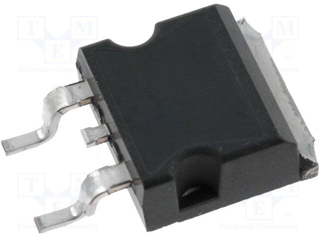
| 产品图片 |
|
| rohs | 符合RoHS无铅 / 符合限制有害物质指令(RoHS)规范要求 |
| 产品系列 | 晶体管,MOSFET,STMicroelectronics STB120NF10T4STripFET™ II |
| 数据手册 | |
| 产品型号 | STB120NF10T4 |
| Pd-PowerDissipation | 312 W |
| Pd-功率耗散 | 312 W |
| RdsOn-Drain-SourceResistance | 10.5 mOhms |
| RdsOn-漏源导通电阻 | 10.5 mOhms |
| Vds-Drain-SourceBreakdownVoltage | 100 V |
| Vds-漏源极击穿电压 | 100 V |
| Vgs-Gate-SourceBreakdownVoltage | +/- 20 V |
| Vgs-栅源极击穿电压 | 20 V |
| 上升时间 | 90 ns |
| 下降时间 | 68 ns |
| 不同Id时的Vgs(th)(最大值) | 4V @ 250µA |
| 不同Vds时的输入电容(Ciss) | 5200pF @ 25V |
| 不同Vgs时的栅极电荷(Qg) | 233nC @ 10V |
| 不同 Id、Vgs时的 RdsOn(最大值) | 10.5 毫欧 @ 60A,10V |
| 产品目录页面 | |
| 产品种类 | MOSFET |
| 供应商器件封装 | D2PAK |
| 其它名称 | 497-2452-1 |
| 其它有关文件 | http://www.st.com/web/catalog/sense_power/FM100/CL824/SC1165/PF67097?referrer=70071840 |
| 典型关闭延迟时间 | 132 ns |
| 功率-最大值 | 312W |
| 包装 | 剪切带 (CT) |
| 商标 | STMicroelectronics |
| 安装类型 | 表面贴装 |
| 安装风格 | SMD/SMT |
| 封装 | Reel |
| 封装/外壳 | TO-263-3,D²Pak(2 引线+接片),TO-263AB |
| 封装/箱体 | D2PAK-2 |
| 工厂包装数量 | 1000 |
| 晶体管极性 | N-Channel |
| 最大工作温度 | + 175 C |
| 最小工作温度 | - 55 C |
| 标准包装 | 1 |
| 正向跨导-最小值 | 90 S |
| 漏源极电压(Vdss) | 100V |
| 电流-连续漏极(Id)(25°C时) | 110A (Tc) |
| 系列 | STB120NF10 |
| 通道模式 | Enhancement |
| 配置 | Single |


PDF Datasheet 数据手册内容提取
STB120NF10T4, STP120NF10, STW120NF10 N-channel 100 V, 9.0 mΩ typ., 110 A STripFET™ II Power MOSFETs in D²PAK, TO-220 and TO-247 packages Datasheet - production data TAB Features Order code VDS RDS(on) max. ID STB120NF10T4 STP120NF10 100 V 10.5 mΩ 110 A D2PAK TAB STW120NF10 Exceptional dv/dt capability 100% avalanche tested 3 3 Low gate charge TO-220 2 2 1 TO-247 1 Applications Figure 1: Internal schematic diagram Switching applications Description D(2,TAB) These Power MOSFETs have been developed using STMicroelectronics’ unique STripFET process, which is specifically designed to minimize input capacitance and gate charge. This renders the devices suitable for use as G(1) primary switch in advanced high-efficiency isolated DC-DC converters for telecom and computer applications, and applications with low gate charge driving requirements. S(3) AM01475v1_noZen Table 1: Device summary Order code Marking Package Packing STB120NF10T4 B120NF10 D2PAK Tape and reel STP120NF10 P120NF10 TO-220 Tube STW120NF10 120NF10 TO-247 November 2017 DocID9522 Rev 8 1/19 This is information on a product in full production. www.st.com
Contents STB120NF10T4, STP120NF10, STW120NF10 Contents 1 Electrical ratings ............................................................................. 3 2 Electrical characteristics ................................................................ 4 2.1 Electrical characteristics (curves) ...................................................... 6 3 Test circuits ..................................................................................... 8 4 Package information ....................................................................... 9 4.1 D²PAK (TO-263) type A2 package information ................................. 9 4.2 D²PAK packing information ............................................................. 12 4.3 TO-220 package information ........................................................... 14 4.4 TO-247 package information ........................................................... 16 5 Revision history ............................................................................ 18 2/19 DocID9522 Rev 8
STB120NF10T4, STP120NF10, STW120NF10 Electrical ratings 1 Electrical ratings Table 2: Absolute maximum ratings Symbol Parameter Value Unit VDS Drain-source voltage 100 V VGS Gate-source voltage ±20 V Drain current (continuous) at TC = 25 °C 110 A ID Drain current (continuous) at TC = 100 °C 77 A IDM(1) Drain current (pulsed) 440 A PTOT Total dissipation at TC = 25 °C 312 W dv/dt(2) Peak diode recovery voltage slope 10 V/ns EAS(3) Single pulse avalanche energy 550 mJ Tj Operating junction temperature range -55 to 175 °C Tstg Storage temperature range Notes: (1)Pulse width is limited by safe operating area. (2)ISD ≤ 110 A, di/dt ≤ 300 A/μs, VDD = 80% V(BR)DSS (3)Starting Tj =25 °C, ID = 60 A, VDD = 50 V Table 3: Thermal data Value Symbol Parameter Unit TO-220 TO-247 D2PAK Rthj-case Thermal resistance junction-case 0.48 °C/W Rthj-amb Thermal resistance junction-ambient 62.5 °C/W Rthj-pcb Thermal resistance junction-pcb(1) 35 °C/W Notes: (1)When mounted on an 1-inch2 FR-4, 2 Oz copper board. DocID9522 Rev 8 3/19
Electrical characteristics STB120NF10T4, STP120NF10, STW120NF10 2 Electrical characteristics (T = 25 °C unless otherwise specified) CASE Table 4: On/off states Symbol Parameter Test conditions Min. Typ. Max. Unit Drain-source breakdown V(BR)DSS voltage VGS = 0 V, ID = 250 µA 100 V VGS = 0 V, VDS = 100 V 1 µA Zero gate voltage drain IDSS current VGS = 0 V, VDS= 100 V, 10 µA Tc = 125 °C(1) IGSS Gate-source leakage current VDS = 0 V, VGS = ±20 V ±100 nA VGS(th) Gate threshold voltage VDS = VGS, ID = 250 µA 2 4 V Static drain-source RDS(on) on-resistance VGS = 10 V, ID = 60 A 9.0 10.5 mΩ Notes: (1)Defined by design, not subject to production test. Table 5: Dynamic Symbol Parameter Test conditions Min. Typ. Max. Unit Ciss Input capacitance 5200 pF Coss Output capacitance VVDGSS == 02 5V V , f = 1 MHz, - 785 pF Crss Reverse transfer capacitance 325 pF Qg Total gate charge VDD = 80 V, ID= 120 A, 172 233(1) nC Qgs Gate-source charge VGS = 0 to 10 V - 32 nC (see Figure 14: "Test circuit for gate charge Qgd Gate-drain charge 64 nC behavior" ) Notes: (1)Defined by design, not subject to production test. Table 6: Switching times Symbol Parameter Test conditions Min. Typ. Max. Unit td(on) Turn-on delay time VDD = 50 V, ID = 60 A, - 25 - ns tr Rise time RG = 4.7 Ω, VGS = 10 V - 90 - ns (see Figure 13: "Test circuit td(off) Turn-off delay time for resistive load switching - 132 - ns times" and Figure 18: tf Fall time "Switching time waveform") - 68 - ns 4/19 DocID9522 Rev 8
STB120NF10T4, STP120NF10, STW120NF10 Electrical characteristics Table 7: Source drain diode Symbol Parameter Test conditions Min. Typ. Max. Unit ISD Source drain current - 110 A Source-drain current ISDM(1) (pulsed) - 440 A VSD(2) Forward on voltage ISD = 120 A, VGS= 0 V - 1.3 V trr Reverse recovery time ISD = 120 A, di/dt = 100 A/µs, - 152 ns Qrr Reverse recovery charge VDD = 40 V, Tj = 150 °C - 760 nC (see Figure 15: "Test circuit for inductive load switching and IRRM Reverse recovery current diode recovery times") - 10 A Notes: (1)Pulse width is limited by safe operating area. (2)Pulsed: pulse duration = 300 µs, duty cycle 1.5% DocID9522 Rev 8 5/19
Electrical characteristics STB120NF10T4, STP120NF10, STW120NF10 2.1 Electrical characteristics (curves) Figure 2: Safe operating area Figure 3: Thermal impedance Figure 4: Output characteristics Figure 5: Transfer characteristics Figure 6: Normalized V(BR)DSS vs temperature Figure 7: Static drain-source on-resistance 6/19 DocID9522 Rev 8
STB120NF10T4, STP120NF10, STW120NF10 Electrical characteristics Figure 8: Gate charge vs gate-source voltage Figure 9: Capacitance variations Figure 10: Normalized gate threshold voltage vs Figure 11: Normalized on-resistance vs temperature temperature Figure 12: Source-drain diode forward characteristics DocID9522 Rev 8 7/19
Test circuits STB120NF10T4, STP120NF10, STW120NF10 3 Test circuits Figure 13: Test circuit for resistive load Figure 14: Test circuit for gate charge switching times behavior Figure 15: Test circuit for inductive load Figure 16: Unclamped inductive load test switching and diode recovery times circuit Figure 17: Unclamped inductive waveform Figure 18: Switching time waveform 8/19 DocID9522 Rev 8
STB120NF10T4, STP120NF10, STW120NF10 Package information 4 Package information In order to meet environmental requirements, ST offers these devices in different grades of ECOPACK® packages, depending on their level of environmental compliance. ECOPACK® specifications, grade definitions and product status are available at: www.st.com. ECOPACK® is an ST trademark. 4.1 D²PAK (TO-263) type A2 package information Figure 19: D²PAK (TO-263) type A2 package outline DocID9522 Rev 8 9/19
Package information STB120NF10T4, STP120NF10, STW120NF10 Table 8: D²PAK (TO-263) type A2 package mechanical data mm Dim. Min. Typ. Max. A 4.40 4.60 A1 0.03 0.23 b 0.70 0.93 b2 1.14 1.70 c 0.45 0.60 c2 1.23 1.36 D 8.95 9.35 D1 7.50 7.75 8.00 D2 1.10 1.30 1.50 E 10.00 10.40 E1 8.70 8.90 9.10 E2 7.30 7.50 7.70 e 2.54 e1 4.88 5.28 H 15.00 15.85 J1 2.49 2.69 L 2.29 2.79 L1 1.27 1.40 L2 1.30 1.75 R 0.40 V2 0° 8° 10/19 DocID9522 Rev 8
STB120NF10T4, STP120NF10, STW120NF10 Package information Figure 20: D²PAK (TO-263) recommended footprint (dimensions are in mm) DocID9522 Rev 8 11/19
Package information STB120NF10T4, STP120NF10, STW120NF10 4.2 D²PAK packing information Figure 21: D²PAK tape outline 12/19 DocID9522 Rev 8
STB120NF10T4, STP120NF10, STW120NF10 Package information Figure 22: D²PAK reel outline Table 9: D²PAK tape and reel mechanical data Tape Reel mm mm Dim. Dim. Min. Max. Min. Max. A0 10.5 10.7 A 330 B0 15.7 15.9 B 1.5 D 1.5 1.6 C 12.8 13.2 D1 1.59 1.61 D 20.2 E 1.65 1.85 G 24.4 26.4 F 11.4 11.6 N 100 K0 4.8 5.0 T 30.4 P0 3.9 4.1 P1 11.9 12.1 Base quantity 1000 P2 1.9 2.1 Bulk quantity 1000 R 50 T 0.25 0.35 W 23.7 24.3 DocID9522 Rev 8 13/19
Package information STB120NF10T4, STP120NF10, STW120NF10 4.3 TO-220 package information Figure 23: TO-220 type A package outline 14/19 DocID9522 Rev 8
STB120NF10T4, STP120NF10, STW120NF10 Package information Table 10: TO-220 type A package mechanical data mm Dim. Min. Typ. Max. A 4.40 4.60 b 0.61 0.88 b1 1.14 1.55 c 0.48 0.70 D 15.25 15.75 D1 1.27 E 10.00 10.40 e 2.40 2.70 e1 4.95 5.15 F 1.23 1.32 H1 6.20 6.60 J1 2.40 2.72 L 13.00 14.00 L1 3.50 3.93 L20 16.40 L30 28.90 øP 3.75 3.85 Q 2.65 2.95 DocID9522 Rev 8 15/19
Package information STB120NF10T4, STP120NF10, STW120NF10 4.4 TO-247 package information Figure 24: TO-247 package outline 16/19 DocID9522 Rev 8
STB120NF10T4, STP120NF10, STW120NF10 Package information Table 11: TO-247 package mechanical data mm Dim. Min. Typ. Max. A 4.85 5.15 A1 2.20 2.60 b 1.0 1.40 b1 2.0 2.40 b2 3.0 3.40 c 0.40 0.80 D 19.85 20.15 E 15.45 15.75 e 5.30 5.45 5.60 L 14.20 14.80 L1 3.70 4.30 L2 18.50 ØP 3.55 3.65 ØR 4.50 5.50 S 5.30 5.50 5.70 DocID9522 Rev 8 17/19
Revision history STB120NF10T4, STP120NF10, STW120NF10 5 Revision history Table 12: Document revision history Date Revision Changes 20-Mar-2006 2 Preliminary datasheet 31-Mar-2006 3 Typing error 19-Jun-2006 4 New template, no content change 28-Jun-2006 5 New ID value on Table 2 05-Oct-2006 6 New value on Table 7 11-May-2011 7 Added new package and mechanical data: TO-220FP Part number STF120NF10 has been moved to a separate datasheet. Updated features, description and device summary on cover page. Updated Table 2: "Absolute maximum ratings", Table 3: "Thermal 03-Nov-2017 8 data" and Table 4: "On/off states". Updated Section 4: "Package information". Minor text changes 18/19 DocID9522 Rev 8
STB120NF10T4, STP120NF10, STW120NF10 IMPORTANT NOTICE – PLEASE READ CAREFULLY STMicroelectronics NV and its subsidiaries (“ST”) reserve the right to make changes, corrections, enhancements, modifications, and improvements to ST products and/or to this document at any time without notice. Purchasers should obtain the latest relevant information on ST products before placing orders. ST products are sold pursuant to ST’s terms and conditions of sale in place at the time of order acknowledgement. Purchasers are solely responsible for the choice, selection, and use of ST products and ST assumes no liability for application assistance or the design of Purchasers’ products. No license, express or implied, to any intellectual property right is granted by ST herein. Resale of ST products with provisions different from the information set forth herein shall void any warranty granted by ST for such product. ST and the ST logo are trademarks of ST. All other product or service names are the property of their respective owners. Information in this document supersedes and replaces information previously supplied in any prior versions of this document. © 2017 STMicroelectronics – All rights reserved DocID9522 Rev 8 19/19