ICGOO在线商城 > 分立半导体产品 > 晶体管 - FET,MOSFET - 单 > NDB6060L
 Datasheet下载
- 型号: NDB6060L
- 制造商: Fairchild Semiconductor
- 库位|库存: xxxx|xxxx
- 要求:
| 数量阶梯 | 香港交货 | 国内含税 |
| +xxxx | $xxxx | ¥xxxx |
查看当月历史价格
查看今年历史价格
NDB6060L产品简介:
ICGOO电子元器件商城为您提供NDB6060L由Fairchild Semiconductor设计生产,在icgoo商城现货销售,并且可以通过原厂、代理商等渠道进行代购。 NDB6060L价格参考。Fairchild SemiconductorNDB6060L封装/规格:晶体管 - FET,MOSFET - 单, 表面贴装 N 沟道 60V 48A(Tc) 100W(Tc) D²PAK(TO-263AB)。您可以下载NDB6060L参考资料、Datasheet数据手册功能说明书,资料中有NDB6060L 详细功能的应用电路图电压和使用方法及教程。
NDB6060L是由ON Semiconductor(现为安森美半导体)生产的单个MOSFET晶体管,具体来说是N沟道增强型MOSFET。它广泛应用于多种电子电路中,尤其是在需要高效开关和功率管理的场景中。

 应用场景

1. 电源管理:
   - NDB6060L常用于直流-直流转换器(DC-DC Converter),如降压、升压或反相转换器。其低导通电阻(Rds(on))使得在高电流应用中能够减少功率损耗,提高效率。
   - 该器件也适用于线性稳压器中的旁路开关,以实现快速响应和稳定的电压输出。

2. 电机控制:
   - 在小型电机驱动电路中,NDB6060L可以作为驱动信号的开关元件,控制电机的启动、停止和调速。
   - 它还可以用于无刷直流电机(BLDC)的逆变器电路中,通过PWM(脉宽调制)控制来调节电机转速和扭矩。

3. 负载开关:
   - 由于其低导通电阻和快速开关特性,NDB6060L非常适合用作负载开关,特别是在便携式设备中,如智能手机、平板电脑和笔记本电脑等,用于管理和保护电池供电系统。

4. 保护电路:
   - NDB6060L可用于过流保护、短路保护和热保护电路中。例如,在USB充电接口中,它可以防止过大的电流通过,从而保护设备免受损坏。
   - 在汽车电子中,该器件可以用于电池管理系统中的开关,确保在异常情况下迅速切断电源,保障安全。

5. 音频放大器:
   - 在D类音频放大器中,NDB6060L可以用作输出级的开关元件,帮助实现高效的音频信号放大,同时减少热量产生。

6. 通信设备:
   - 在基站和其他通信设备中,NDB6060L可以用于射频前端模块中的开关,以实现快速切换和信号处理。

总之,NDB6060L凭借其优异的电气性能和可靠性,广泛应用于各种需要高效开关和功率管理的领域,尤其适合对能效和稳定性有较高要求的应用。
| 参数 | 数值 |
| 产品目录 | |
| ChannelMode | Enhancement |
| 描述 | MOSFET N-CH 60V 48A TO-263ABMOSFET N-Ch LL FET Enhancement Mode |
| 产品分类 | FET - 单分离式半导体 |
| FET功能 | 逻辑电平门 |
| FET类型 | MOSFET N 通道,金属氧化物 |
| Id-ContinuousDrainCurrent | 48 A |
| Id-连续漏极电流 | 48 A |
| 品牌 | Fairchild Semiconductor |
| 产品手册 | |
| 产品图片 |
|
| rohs | RoHS 合规性豁免无铅 / 符合限制有害物质指令(RoHS)规范要求 |
| 产品系列 | 晶体管,MOSFET,Fairchild Semiconductor NDB6060L- |
| 数据手册 | |
| 产品型号 | NDB6060L |
| PCN封装 | |
| Pd-PowerDissipation | 100 W |
| Pd-功率耗散 | 100 W |
| RdsOn-Drain-SourceResistance | 20 mOhms |
| RdsOn-漏源导通电阻 | 20 mOhms |
| Vds-Drain-SourceBreakdownVoltage | 60 V |
| Vds-漏源极击穿电压 | 60 V |
| Vgs-Gate-SourceBreakdownVoltage | +/- 16 V |
| Vgs-栅源极击穿电压 | 16 V |
| 上升时间 | 320 ns |
| 下降时间 | 161 ns |
| 不同Id时的Vgs(th)(最大值) | 2V @ 250µA |
| 不同Vds时的输入电容(Ciss) | 2000pF @ 25V |
| 不同Vgs时的栅极电荷(Qg) | 60nC @ 5V |
| 不同 Id、Vgs时的 RdsOn(最大值) | 20 毫欧 @ 24A,10V |
| 产品培训模块 | http://www.digikey.cn/PTM/IndividualPTM.page?site=cn&lang=zhs&ptm=356http://www.digikey.cn/PTM/IndividualPTM.page?site=cn&lang=zhs&ptm=6736 |
| 产品目录页面 | |
| 产品种类 | MOSFET |
| 供应商器件封装 | TO-263AB |
| 其它名称 | NDB6060LTR |
| 典型关闭延迟时间 | 49 ns |
| 功率-最大值 | 100W |
| 包装 | 带卷 (TR) |
| 单位重量 | 1.312 g |
| 商标 | Fairchild Semiconductor |
| 安装类型 | 表面贴装 |
| 安装风格 | SMD/SMT |
| 封装 | Reel |
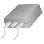
| 封装/外壳 | TO-263-3,D²Pak(2 引线+接片),TO-263AB |
| 封装/箱体 | D2PAK-2 |
| 工厂包装数量 | 800 |
| 晶体管极性 | N-Channel |
| 最大工作温度 | + 175 C |
| 最小工作温度 | - 65 C |
| 标准包装 | 800 |
| 漏源极电压(Vdss) | 60V |
| 电流-连续漏极(Id)(25°C时) | 48A (Tc) |
| 系列 | NDB6060 |
| 通道模式 | Enhancement |
| 配置 | Single |
| 零件号别名 | NDB6060L_NL |


- 商务部:美国ITC正式对集成电路等产品启动337调查
- 曝三星4nm工艺存在良率问题 高通将骁龙8 Gen1或转产台积电
- 太阳诱电将投资9.5亿元在常州建新厂生产MLCC 预计2023年完工
- 英特尔发布欧洲新工厂建设计划 深化IDM 2.0 战略
- 台积电先进制程称霸业界 有大客户加持明年业绩稳了
- 达到5530亿美元!SIA预计今年全球半导体销售额将创下新高
- 英特尔拟将自动驾驶子公司Mobileye上市 估值或超500亿美元
- 三星加码芯片和SET,合并消费电子和移动部门,撤换高东真等 CEO
- 三星电子宣布重大人事变动 还合并消费电子和移动部门
- 海关总署:前11个月进口集成电路产品价值2.52万亿元 增长14.8%


PDF Datasheet 数据手册内容提取
Is Now Part of To learn more about ON Semiconductor, please visit our website at www.onsemi.com Please note: As part of the Fairchild Semiconductor integration, some of the Fairchild orderable part numbers will need to change in order to meet ON Semiconductor’s system requirements. Since the ON Semiconductor product management systems do not have the ability to manage part nomenclature that utilizes an underscore (_), the underscore (_) in the Fairchild part numbers will be changed to a dash (-). This document may contain device numbers with an underscore (_). Please check the ON Semiconductor website to verify the updated device numbers. The most current and up-to-date ordering information can be found at www.onsemi.com. Please email any questions regarding the system integration to Fairchild_questions@onsemi.com. ON Semiconductor and the ON Semiconductor logo are trademarks of Semiconductor Components Industries, LLC dba ON Semiconductor or its subsidiaries in the United States and/or other countries. ON Semiconductor owns the rights to a number of patents, trademarks, copyrights, trade secrets, and other intellectual property. A listing of ON Semiconductor’s product/patent coverage may be accessed at www.onsemi.com/site/pdf/Patent-Marking.pdf. ON Semiconductor reserves the right to make changes without further notice to any products herein. ON Semiconductor makes no warranty, representation or guarantee regarding the suitability of its products for any particular purpose, nor does ON Semiconductor assume any liability arising out of the application or use of any product or circuit, and specifically disclaims any and all liability, including without limitation special, consequential or incidental damages. Buyer is responsible for its products and applications using ON Semiconductor products, including compliance with all laws, regulations and safety requirements or standards, regardless of any support or applications information provided by ON Semiconductor. “Typical” parameters which may be provided in ON Semiconductor data sheets and/or specifications can and do vary in different applications and actual performance may vary over time. All operating parameters, including “Typicals” must be validated for each customer application by customer’s technical experts. ON Semiconductor does not convey any license under its patent rights nor the rights of others. ON Semiconductor products are not designed, intended, or authorized for use as a critical component in life support systems or any FDA Class 3 medical devices or medical devices with a same or similar classification in a foreign jurisdiction or any devices intended for implantation in the human body. Should Buyer purchase or use ON Semiconductor products for any such unintended or unauthorized application, Buyer shall indemnify and hold ON Semiconductor and its officers, employees, subsidiaries, affiliates, and distributors harmless against all claims, costs, damages, and expenses, and reasonable attorney fees arising out of, directly or indirectly, any claim of personal injury or death associated with such unintended or unauthorized use, even if such claim alleges that ON Semiconductor was negligent regarding the design or manufacture of the part. ON Semiconductor is an Equal Opportunity/Affirmative Action Employer. This literature is subject to all applicable copyright laws and is not for resale in any manner.
April 1996 NDP6060L / NDB6060L N-Channel Logic Level Enhancement Mode Field Effect Transistor General Description Features These logic level N-Channel enhancement mode power 48A, 60V. R = 0.025W @ V = 5V. DS(ON) GS field effect transistors are produced using Fairchild's Low drive requirements allowing operation directly from logic proprietary, high cell density, DMOS technology. This drivers. V < 2.0V. very high density process has been especially tailored to GS(TH) minimize on-state resistance, provide superior switching Critical DC electrical parameters specified at elevated performance, and withstand high energy pulses in the temperature. avalanche and commutation modes. These devices are Rugged internal source-drain diode can eliminate the need particularly suited for low voltage applications such as for an external Zener diode transient suppressor. automotive, DC/DC converters, PWM motor controls, and other battery powered circuits where fast switching, 175°C maximum junction temperature rating. low in-line power loss, and resistance to transients are High density cell design for extremely low R . needed. DS(ON) TO-220 and TO-263 (D2PAK) package for both through hole and surface mount applications. ________________________________________________________________________________ D G S Absolute Maximum Ratings T = 25°C unless otherwise noted C Symbol Parameter NDP6060L NDB6060L Units V Drain-Source Voltage 60 V DSS V Drain-Gate Voltage (R < 1 MW ) 60 V DGR GS V Gate-Source Voltage - Continuous ± 16 V GSS - Nonrepetitive (t < 50 µs) ± 25 P I Drain Current - Continuous 48 A D - Pulsed 144 P Total Power Dissipation @ T = 25°C 100 W D C Derate above 25°C 0.67 W/°C T,T Operating and Storage Temperature -65 to 175 °C J STG T Maximum lead temperature for soldering 275 °C L purposes, 1/8" from case for 5 seconds © 1997 Fairchild Semiconductor Corporation NDP6060L Rev. D / NDB6060L Rev. E
Electrical Characteristics (T = 25°C unless otherwise noted) C Symbol Parameter Conditions Min Typ Max Units DRAIN-SOURCE AVALANCHE RATINGS (Note 1) W Single Pulse Drain-Source Avalanche V = 25 V, I = 48 A 200 mJ DSS DD D Energy I Maximum Drain-Source Avalanche Current 48 A AR OFF CHARACTERISTICS BV Drain-Source Breakdown Voltage V = 0 V, I = 250 µA 60 V DSS GS D I Zero Gate Voltage Drain Current V = 60 V, V = 0 V 250 µA DSS DS GS T = 125°C 1 mA J I Gate - Body Leakage, Forward V = 16 V, V = 0 V 100 nA GSSF GS DS I Gate - Body Leakage, Reverse V = -16 V, V = 0 V -100 nA GSSR GS DS ON CHARACTERISTICS (Note 1) V Gate Threshold Voltage V = V , I = 250 µA 1 2 V GS(th) DS GS D T = 125°C 0.65 1.5 J R Static Drain-Source On-Resistance V = 5 V, I = 24 A 0.025 W DS(ON) GS D T = 125°C 0.04 J V = 10 V, I = 24 A 0.02 GS D I On-State Drain Current V = 5 V, V = 10 V 48 A D(on) GS DS g Forward Transconductance V = 10 V, I = 24 A 10 S FS DS D DYNAMIC CHARACTERISTICS C Input Capacitance V = 25 V, V = 0 V, 1630 2000 pF iss DS GS f = 1.0 MHz C Output Capacitance 460 800 pF oss C Reverse Transfer Capacitance 150 400 pF rss SWITCHING CHARACTERISTICS (Note 1) t Turn - On Delay Time V = 30 V, I = 48 A, 15 30 nS D(on) DD D tr Turn - On Rise Time VRGS == 51 5V ,W RGEN = 15 W , 320 500 nS GS t Turn - Off Delay Time 49 100 nS D(off) t Turn - Off Fall Time 161 300 nS f Q Total Gate Charge V = 48 V, 36 60 nC g DS I = 48 A, V = 5 V Q Gate-Source Charge D GS 8.2 nC gs Q Gate-Drain Charge 21 nC gd NDP6060L Rev. D / NDB6060L Rev. E
Electrical Characteristics (T = 25°C unless otherwise noted) C Symbol Parameter Conditions Min Typ Max Units DRAIN-SOURCE DIODE CHARACTERISTICS I Maximum Continuos Drain-Source Diode Forward Current 48 A S I Maximum Pulsed Drain-Source Diode Forward Current 144 A SM VSD Drain-Source Diode Forward Voltage VGS = 0 V, IS = 24 A (Note 1) 1.3 V T = 125°C 1.2 J trr Reverse Recovery Time VdIGS/d =t 0= V1,0 0IF A =/ µ4s8 A, 35 75 140 ns I Reverse Recovery Current F 2 3.6 8 A rr THERMAL CHARACTERISTICS Rq JC Thermal Resistance, Junction-to-Case 1.5 °C/W Rq JA Thermal Resistance, Junction-to-Ambient 62.5 °C/W Note: 1. Pulse Test: Pulse Width < 300 µs, Duty Cycle < 2.0%. NDP6060L Rev. D / NDB6060L Rev. E
Typical Electrical Characteristics 100 2 V = 10V GS 6.0 VG S = 3.0V E CURRENT (A) 6800 5.0 4.5 4.0 MALIZED N-RESISTANCE1.5 3.5 4.0 4.5 5.0 I , DRAIN-SOURCD 2400 3.5 3.0 2.5 R , NORDS(on)DRAIN-SOURCE O 1 5.5 6.0 10 0 0.5 0 1 2 3 4 5 0 20 40 60 80 100 VD S , DRAIN-SOURCE VOLTAGE (V) I D , DRAIN CURRENT (A) Figure 1. On-Region Characteristics. Figure 2. On-Resistance Variation with Gate Voltage and Drain Current. 2 2 V = 5.0V R , NORMALIZEDDS(ON) DRAIN-SOURCE ON-RESISTANCE011...1727.15555 VI D G S = =2 45AV R , NORMALIZEDDS(on) DRAIN-SOURCE ON-RESISTANCE01111.....824681 GS TJ = 125°C 25°C -55°C 0.5-50 -25 0 25 50 75 100 125 150 175 0.60 20 40 60 80 100 T J , JUNCTION TEMPERATURE (°C) I D , DRAIN CURRENT (A) Figure 3. On-Resistance Variation Figure 4. On-Resistance Variation with Drain with Temperature. Current and Temperature. 60 1.3 I , DRAIN CURRENT (A)D1234500000 VD S = 10V TJ = -55°C 25°C 125°C V , NORMALIZEDGS(th)TE-SOURCE THRESHOLD VOLTAGE000011......1678912 I DV D =S 2=5 V0GµSA A G 0 0.5 1 2 3 4 5 -50 -25 0 25 50 75 100 125 150 175 VG S , GATE TO SOURCE VOLTAGE (V) TJ , JUNCTION TEMPERATURE (°C) Figure 5. Transfer Characteristics. Figure 6. Gate Threshold Variation with Temperature. NDP6060L Rev. D / NDB6060L Rev. E
Typical Electrical Characteristics (continued) 1.15 80 I = 250µA E D BV , NORMALIZEDSSDDRAIN-SOURCE BREAKDOWN VOLTAG01..190.5511 I , REVERSE DRAIN CURRENT (A)S 0.00.0100.10111 TJ = 125°C 25°C -55°C V G S = 0V 0.9 -50 -25 0 25 50 75 100 125 150 175 0.0001 TJ , JUNCTION TEMPERATURE (°C) 0.2 0.4V S D 0, .B6ODY D0.I8ODE FO1RWAR1D. 2VOLTA1G.4E (V)1.6 1.8 Figure 7. Breakdown Voltage Variation with Figure 8. Body Diode Forward Voltage Temperature. Variation with Current and Temperature. 4000 10 3000 I D = 48A V D S = 12V 48V 2000 Ci s s V) 8 E ( CAPACITANCE (pF) 1350000000 f = 1 MHz Co ss ATE-SOURCE VOLTAG 46 24V 200 VG S = 0V C r ss V , GGS 2 100 0 1 2 3 5 10 20 30 50 0 20 40 60 80 VD S , DRAIN TO SOURCE VOLTAGE (V) Q g , GATE CHARGE (nC) Figure 9. Capacitance Characteristics. Figure 10. Gate Charge Characteristics. V t t DD on off td(on) tr td(off) tf V R IN L 90% 90% D V OUT V V OUT GEN 10% 10% R GEN G DUT INVERTED 90% RGS S VIN 50% 50% 10% PULSE WIDTH Figure 11. Switching Test Circuit. Figure 12. Switching Waveforms. NDP6060L Rev. D / NDB6060L Rev. E
Typical Electrical Characteristics (continued) 40 300 ANSCONDUCTANCE (SIEMENS) 123000 T J = -55°C 25°C 125°C I , DRAIN CURRENT (A)D1212500500000 RDS(ORSN Iq)N J VCL GiG m= LS i t E1 = .P5 5U o VCLS/WE D1C0 01m0ms 1sm 1s00µs 10µs g , TRFS 0 V D S =10V 12 T C = 25°C 0 10 20 30 40 1 2 3 5 10 20 30 60 100 ID , DRAIN CURRENT (A) V D S , DRAIN-SOURCE VOLTAGE (V) Figure 13. Transconductance Variation with Figure 14. Maximum Safe Operating. Area Drain Current. and Temperature 1 D = 0.5 E 0.5 C E N ED EFFECTIV MAL RESISTA 000...123 0.1 0.2 R q R J C q J (C t ) == r1(t.)5 *° C R/Wq J C r(t), NORMALIZ ANSIENT THER000...000235 000...000512 Single Pulse P(pk)TJ - T t1 C t= 2 P * R q J C (t) TR Duty Cycle, D = t 1 /t2 0.01 0.01 0.02 0.05 0.1 0.2 0.5 1 2 5 10 20 50 100 200 500 1000 t 1 ,TIME (ms) Figure 15. Transient Thermal Response Curve. NDP6060L Rev. D / NDB6060L Rev. E
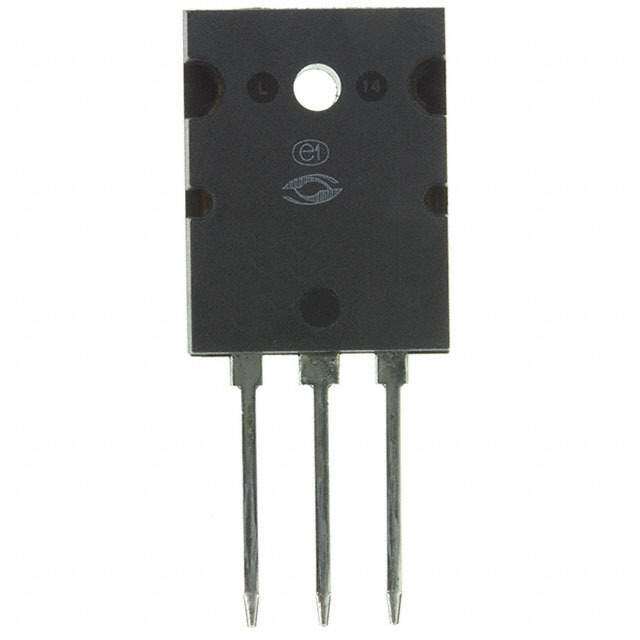
TO-220 Tape and Reel Data and Package Dimensions TO-220 Tube Packing Configuration: Figure 1.0 Packaging Description: TO-220 parts are shipped normally in tube. The tube is made of PVC plastic treated with anti-static agent.These tubes in standard option are placed inside a dissipative 45 units per Tube plastic bag, barcode labeled, and placed inside a box made of recyclable corrugated paper. One box contains two bags maximum (see fig. 1.0). And one or several of these boxes are placed inside a labeled shipping box which comes in different sizes depending on the number of parts shipped. The other option comes in bulk as described in the Packaging Information table. The units in this option are placed inside a small box laid with anti- static bubble sheet. These smaller boxes are individually 12 Tubes per Bag labeled and placed inside a larger box (see fig. 3.0). These larger or intermediate boxes then will be placed finally inside a labeled shipping box which still comes in different sizes depending on the number of units shipped. 530mm x 130mm x 83mm Intermediate box 2 bags per Box Conductive Plastic Bag TO-220 Packaging FSCINT Label sample Information: Figure 2.0 FAIRCHILD SEMICONDUCTOR CORPORATION HTB:B 1080 units maximum LOT: CBVK741B019 QTY: 1080 quantity per box TO-220 Packaging Information NSID: FDP7060 SPEC: Packaging Option (noS tfalonwd acordde) S62Z Packaging type Rail/Tube BULK D/C1: D 9842 SPQEAC RREEVV:: B2 Qty per Tube/Box 45 300 FSCINT Label Box Dimension (mm) 530x130x83 114x102x51 (FSCINT) Max qty per Box 1,080 1,500 Weight per unit (gm) 1.4378 1.4378 Note/Comments TO-220 bulk Packing Configuration: Figure 3.0 Anti-static 530mm x 130mm x 83mm FSCINT Label Bubble Sheets Intermediate box 1500 units maximum quantity per intermediate box 300 units per 5 EO70 boxes per per EO70 box Intermediate Box 114mm x 102mm x 51mm EO70 Immediate Box FSCINT Label TO-220 Tube Configuration: Figure 4.0 0.123 +0.001 0.165 -0.003 Note: All dimensions are in inches 0.080 0.450 0.275 –.030 FN9D8P542060L FN9D8P542060L FN9D8P542060L FN9D8P542060L FN9D8P542060L FN9D8P542060L FN9D8P542060L FN9D8P542060L FN9D8P542060LFN9D8P542060L FN9D8P542060L FN9D8P542060L 1.300 –.015 0.032 0.160 –.003 20.000 +0.031 0.800 -0.065 0.275 August 1999, Rev. B
TO-220 Tape and Reel Data and Package Dimensions, continued TO-220 (FS PKG Code 37) 1:1 Scale 1:1 on letter size paper Dimensions shown below are in: inches [millimeters] Part Weight per unit (gram): 1.4378 September 1998, Rev. A
TO-263AB/D2PAK Tape and Reel Data and Package Dimensions TO-263AB/D2PAK Packaging Configuration: Figure 1.0 Packaging Description: TO-263/D2PAK parts are shipped in tape. The carrier tape ETPPDLNTEOER E NCNLTO UDR TSMO A S ST MBT HR EAIE EE PEG R NNON L RE G EST SIT CT CIOH, T MR TMMAEIVG NIARNNEXEE OA_ TR_ _IC _SDS_ _OT_TER_R_O_ R_AV_N_AG__TID_ _CIEO_IL_CA_EE_C_C_T_ST_IVR__EO gg SFmmTIEAssLTDICS Antistatic Cover Tape irAased dshhmineea.ss diTivveehe e fi lrnaco yomneva re,ta ur rsteaed)pai seplsar inpiimsta, ta aivra iemlny d u(c cltoaailmranbytpoie-onsrs t aeffitidllimlce od f(s) H ppeproaaolyytly eecAdsact retbairvo gafneitlamentdte,. ESD Label T80h0e suen irtese pleedr 1p3a"r tso r in3 3s0tcamnd adriadm oeptteior nr eaerl.e Tshheip rpeeedls wairteh dark blue in color and is made of polystyrene plastic (anti- static coated). This and some other options are further described in the Packaging Information table. These full reels are individually barcode labeled, dry packed, and placed inside a standard intermediate box (illustrated in figure 1.0) made of recyclable corrugated brown paper. One box contains one reel maximum. And CAUTION tbhoexs ew bhoicxhe sc aorme epsl acine dd iinffseirdeen ta sbiazrecso ddee plaebnedleindg shoinp ptihneg number of parts shipped. Static Dissipative Embossed Carrier Tape Moisture Sensitive Label F63TNR Label Customized Label LA306BDF LA306BDF LA306BDF LA306BDF 5389F 5389F 5389F 5389F TO-263AB/D2PAK Packaging Information Packaging Option (noS ftlaonwd acordde) L86Z TO-263AB/D2PAK Unit Orientation Packaging type TNR Rail/Tube Qty per Reel/Tube/Bag 800 45 Reel Size 13" Dia - Box Dimension (mm) 359x359x57 530x130x83 Max qty per Box 800 1,080 359mm x 359mm x 57mm Weight per unit (gm) 1.4378 1.4378 Standard Intermediate box Weight per Reel 1.6050 - Note/Comments ESD Label Moisture Sensitive Label F63TNR Label sample F63TNR Label LOT: CBVK741B019 QTY: 800 FSID: FDB6320L SPEC: DRYPACK Bag D/C1: D9842 QTY1: SPEC REV: D/C2: QTY2: CPN: N/F: F (F63TNR)3 TO-263AB/D2PAK Tape Leader and Trailer Configuration: Figure 2.0 Carrier Tape Components Cover Tape Trailer Tape Leader Tape 400mm minimum or 1520mm minimum or 25 empty pockets 95 empty pockets September 1999, Rev. B
TO-263AB/D2PAK Tape and Reel Data and Package Dimensions, continued TO-263AB/D2PAK Embossed Carrier Tape Configuration: Figure 3.0 P0 D0 T E1 F K0 E2 W Wc B0 Tc A0 P1 D1 User Direction of Feed Dimensions are in millimeter Pkg type A0 B0 W D0 D1 E1 E2 F P1 P0 K0 T Wc Tc TO263AB/ D2PAK 10.60 15.80 24.0 1.55 1.60 1.75 22.25 11.50 16.0 4.0 4.90 0.450 21.0 0.06 +/-0.10 +/-0.10 +/-0.3 +/-0.05 +/-0.10 +/-0.10 min +/-0.10 +/-0.1 +/-0.1 +/-0.10 +/-0.150 +/-0.3 +/-0.02 (24mm) Notes: A0, B0, and K0 dimensions are determined with respect to the EIA/Jedec RS-481 rotational and lateral movement requirements (see sketches A, B, and C). 0.9mm 10 deg maximum maximum Typical component cavity 0.9mm B0 center line maximum 10 deg maximum component rotation Typical Sketch A (Side or Front Sectional View) component Sketch C (Top View) Component Rotation A0 center line Component lateral movement TO-263AB/D2PAK Reel Configuration: SCkoemtchp Bo n(Teonpt V Rieowt)ation Figure 4.0 W1 Measured at Hub Dim A Max B Min Dim C Dim A max Dim N Dim D min DETAIL AA See detail AA W3 13" Diameter Option W2 max Measured at Hub Dimensions are in inches and millimeters Reel Tape Size Dim A Dim B Dim C Dim D Dim N Dim W1 Dim W2 Dim W3 (LSL-USL) Option 24mm 13" Dia 1333.000 01..0559 51132 + +00.5.0/-200.2/-0.008 02.07.925 41.0000 02.49.641 + +2/00.078/-0.000 13.01.947 02.39.491 – – 2 07..14.079 August 1999, Rev. B
TO-263AB/D2PAK Tape and Reel Data and Package Dimensions, continued TO-263AB/D2PAK (FS PKG Code 45) 1:1 Scale 1:1 on letter size paper Dimensions shown below are in: inches [millimeters] Part Weight per unit (gram): 1.4378 August 1998, Rev. A
TRADEMARKS The following are registered and unregistered trademarks Fairchild Semiconductor owns or is authorized to use and is not intended to be an exhaustive list of all such trademarks. ACEx™ ISOPLANAR™ SyncFET™ CoolFET™ MICROWIRE™ TinyLogic™ CROSSVOLT™ POP™ UHC™ E2CMOSTM PowerTrench VCX™ FACT™ QFET™ FACT Quiet Series™ QS™ FAST® Quiet Series™ FASTr™ SuperSOT™-3 GTO™ SuperSOT™-6 HiSeC™ SuperSOT™-8 DISCLAIMER FAIRCHILD SEMICONDUCTOR RESERVES THE RIGHT TO MAKE CHANGES WITHOUT FURTHER NOTICE TO ANY PRODUCTS HEREIN TO IMPROVE RELIABILITY, FUNCTION OR DESIGN. FAIRCHILD DOES NOT ASSUME ANY LIABILITY ARISING OUT OF THE APPLICATION OR USE OF ANY PRODUCT OR CIRCUIT DESCRIBED HEREIN; NEITHER DOES IT CONVEY ANY LICENSE UNDER ITS PATENT RIGHTS, NOR THE RIGHTS OF OTHERS. LIFE SUPPORT POLICY FAIRCHILD’S PRODUCTS ARE NOT AUTHORIZED FOR USE AS CRITICAL COMPONENTS IN LIFE SUPPORT DEVICES OR SYSTEMS WITHOUT THE EXPRESS WRITTEN APPROVAL OF FAIRCHILD SEMICONDUCTOR CORPORATION. As used herein: 1. Life support devices or systems are devices or 2. A critical component is any component of a life systems which, (a) are intended for surgical implant into support device or system whose failure to perform can the body, or (b) support or sustain life, or (c) whose be reasonably expected to cause the failure of the life failure to perform when properly used in accordance support device or system, or to affect its safety or with instructions for use provided in the labeling, can be effectiveness. reasonably expected to result in significant injury to the user. PRODUCT STATUS DEFINITIONS Definition of Terms Datasheet Identification Product Status Definition Advance Information Formative or This datasheet contains the design specifications for In Design product development. Specifications may change in any manner without notice. Preliminary First Production This datasheet contains preliminary data, and supplementary data will be published at a later date. Fairchild Semiconductor reserves the right to make changes at any time without notice in order to improve design. No Identification Needed Full Production This datasheet contains final specifications. Fairchild Semiconductor reserves the right to make changes at any time without notice in order to improve design. Obsolete Not In Production This datasheet contains specifications on a product that has been discontinued by Fairchild semiconductor. The datasheet is printed for reference information only. Rev. D
ON Semiconductor and are trademarks of Semiconductor Components Industries, LLC dba ON Semiconductor or its subsidiaries in the United States and/or other countries. ON Semiconductor owns the rights to a number of patents, trademarks, copyrights, trade secrets, and other intellectual property. A listing of ON Semiconductor’s product/patent coverage may be accessed at www.onsemi.com/site/pdf/Patent−Marking.pdf. ON Semiconductor reserves the right to make changes without further notice to any products herein. ON Semiconductor makes no warranty, representation or guarantee regarding the suitability of its products for any particular purpose, nor does ON Semiconductor assume any liability arising out of the application or use of any product or circuit, and specifically disclaims any and all liability, including without limitation special, consequential or incidental damages. Buyer is responsible for its products and applications using ON Semiconductor products, including compliance with all laws, regulations and safety requirements or standards, regardless of any support or applications information provided by ON Semiconductor. “Typical” parameters which may be provided in ON Semiconductor data sheets and/or specifications can and do vary in different applications and actual performance may vary over time. All operating parameters, including “Typicals” must be validated for each customer application by customer’s technical experts. ON Semiconductor does not convey any license under its patent rights nor the rights of others. ON Semiconductor products are not designed, intended, or authorized for use as a critical component in life support systems or any FDA Class 3 medical devices or medical devices with a same or similar classification in a foreign jurisdiction or any devices intended for implantation in the human body. Should Buyer purchase or use ON Semiconductor products for any such unintended or unauthorized application, Buyer shall indemnify and hold ON Semiconductor and its officers, employees, subsidiaries, affiliates, and distributors harmless against all claims, costs, damages, and expenses, and reasonable attorney fees arising out of, directly or indirectly, any claim of personal injury or death associated with such unintended or unauthorized use, even if such claim alleges that ON Semiconductor was negligent regarding the design or manufacture of the part. ON Semiconductor is an Equal Opportunity/Affirmative Action Employer. This literature is subject to all applicable copyright laws and is not for resale in any manner. PUBLICATION ORDERING INFORMATION LITERATURE FULFILLMENT: N. American Technical Support: 800−282−9855 Toll Free ON Semiconductor Website: www.onsemi.com Literature Distribution Center for ON Semiconductor USA/Canada 19521 E. 32nd Pkwy, Aurora, Colorado 80011 USA Europe, Middle East and Africa Technical Support: Order Literature: http://www.onsemi.com/orderlit Phone: 303−675−2175 or 800−344−3860 Toll Free USA/Canada Phone: 421 33 790 2910 Fax: 303−675−2176 or 800−344−3867 Toll Free USA/Canada Japan Customer Focus Center For additional information, please contact your local Email: orderlit@onsemi.com Phone: 81−3−5817−1050 Sales Representative © Semiconductor Components Industries, LLC www.onsemi.com www.onsemi.com 1
Mouser Electronics Authorized Distributor Click to View Pricing, Inventory, Delivery & Lifecycle Information: O N Semiconductor: NDB6060L