ICGOO在线商城 > 分立半导体产品 > 晶体管 - FET,MOSFET - 单 > FDB2572

 Datasheet下载
- 型号: FDB2572
- 制造商: Fairchild Semiconductor
- 库位|库存: xxxx|xxxx
- 要求:
| 数量阶梯 | 香港交货 | 国内含税 |
| +xxxx | $xxxx | ¥xxxx |
查看当月历史价格
查看今年历史价格
FDB2572产品简介:
ICGOO电子元器件商城为您提供FDB2572由Fairchild Semiconductor设计生产,在icgoo商城现货销售,并且可以通过原厂、代理商等渠道进行代购。 FDB2572价格参考。Fairchild SemiconductorFDB2572封装/规格:晶体管 - FET,MOSFET - 单, 表面贴装 N 沟道 150V 4A(Ta),29A(Tc) 135W(Tc) TO-236AB。您可以下载FDB2572参考资料、Datasheet数据手册功能说明书,资料中有FDB2572 详细功能的应用电路图电压和使用方法及教程。
FDB2572 是由 ON Semiconductor(安森美半导体)生产的单通道 MOSFET(金属氧化物场效应晶体管)。该型号属于 FET 类别,广泛应用于多种电力电子设备和电路设计中。以下是其主要应用场景:

1. 电源管理:
   - FDB2572 常用于开关电源(SMPS)、DC-DC 转换器、AC-DC 适配器等电源管理系统中。其低导通电阻(Rds(on))特性有助于提高效率,减少功率损耗,适用于需要高效能转换的应用。

2. 电机驱动:
   - 在小型电机驱动电路中,如无刷直流电机(BLDC)、步进电机等,FDB2572 可作为功率级元件,实现精确的电流控制和快速响应。其高开关速度和低损耗特性使其适合高频驱动应用。

3. 负载开关:
   - 作为负载开关,FDB2572 可用于笔记本电脑、平板电脑、智能手机等便携式设备中,提供高效的电源管理和保护功能。它能够快速切换负载状态,确保系统的稳定性和安全性。

4. 电池管理系统 (BMS):
   - 在电池管理系统中,FDB2572 可用于电池充放电控制、过流保护、短路保护等功能。其低导通电阻和高可靠性确保了电池的安全运行和长寿命。

5. 汽车电子:
   - 在汽车电子领域,FDB2572 可用于车载充电器、电动助力转向系统(EPS)、车身控制系统等。其耐高温、抗干扰能力强的特点使其适合严苛的车规环境。

6. 工业自动化:
   - 在工业自动化设备中,如可编程逻辑控制器(PLC)、伺服驱动器等,FDB2572 可用于信号隔离、功率放大等环节。其高可靠性和稳定性保证了工业设备的长期可靠运行。

总之,FDB2572 凭借其优异的电气性能和可靠性,在多个领域的电力电子应用中表现出色,适用于需要高效、低损耗、高可靠性的电路设计。
| 参数 | 数值 |
| 产品目录 | |
| ChannelMode | Enhancement |
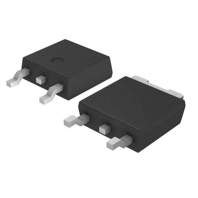
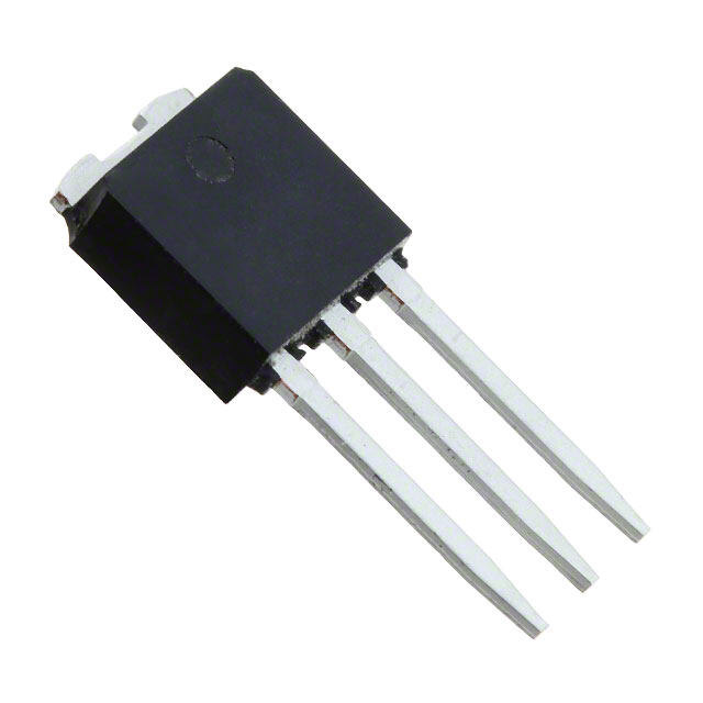
| 描述 | MOSFET N-CH 150V 29A TO-263ABMOSFET N-Channel UltraFET |
| 产品分类 | FET - 单分离式半导体 |
| FET功能 | 标准 |
| FET类型 | MOSFET N 通道,金属氧化物 |
| Id-ContinuousDrainCurrent | 29 A |
| 品牌 | Fairchild Semiconductor |
| 产品手册 | |
| 产品图片 |
|
| rohs | RoHS 合规性豁免无铅 / 符合限制有害物质指令(RoHS)规范要求 |
| 产品系列 | 晶体管,MOSFET,Fairchild Semiconductor FDB2572PowerTrench® |
| 数据手册 | |
| 产品型号 | FDB2572 |
| Pd-PowerDissipation | 135 W |
| RdsOn-Drain-SourceResistance | 45 mOhms |
| Vds-Drain-SourceBreakdownVoltage | 150 V |
| Vgs-Gate-SourceBreakdownVoltage | +/- 20 V |
| 上升时间 | 14 ns |
| 下降时间 | 14 ns |
| 不同Id时的Vgs(th)(最大值) | 4V @ 250µA |
| 不同Vds时的输入电容(Ciss) | 1770pF @ 25V |
| 不同Vgs时的栅极电荷(Qg) | 34nC @ 10V |
| 不同 Id、Vgs时的 RdsOn(最大值) | 54 毫欧 @ 9A,10V |
| 产品培训模块 | http://www.digikey.cn/PTM/IndividualPTM.page?site=cn&lang=zhs&ptm=356 |
| 产品种类 | MOSFET |
| 供应商器件封装 | TO-263AB |
| 其它名称 | FDB2572DKR |
| 典型关闭延迟时间 | 31 ns |
| 功率-最大值 | 135W |
| 包装 | Digi-Reel® |
| 单位重量 | 1.312 g |
| 商标 | Fairchild Semiconductor |
| 安装类型 | 表面贴装 |
| 安装风格 | SMD/SMT |
| 封装 | Reel |
| 封装/外壳 | TO-263-3,D²Pak(2 引线+接片),TO-263AB |
| 封装/箱体 | TO-263 |
| 工厂包装数量 | 800 |
| 晶体管极性 | N-Channel |
| 最大工作温度 | + 175 C |
| 最小工作温度 | - 55 C |
| 标准包装 | 1 |
| 漏源极电压(Vdss) | 150V |
| 电流-连续漏极(Id)(25°C时) | 4A (Ta), 29A (Tc) |
| 系列 | FDB2572 |
| 配置 | Single |
| 零件号别名 | FDB2572_NL |


- 商务部:美国ITC正式对集成电路等产品启动337调查
- 曝三星4nm工艺存在良率问题 高通将骁龙8 Gen1或转产台积电
- 太阳诱电将投资9.5亿元在常州建新厂生产MLCC 预计2023年完工
- 英特尔发布欧洲新工厂建设计划 深化IDM 2.0 战略
- 台积电先进制程称霸业界 有大客户加持明年业绩稳了
- 达到5530亿美元!SIA预计今年全球半导体销售额将创下新高
- 英特尔拟将自动驾驶子公司Mobileye上市 估值或超500亿美元
- 三星加码芯片和SET,合并消费电子和移动部门,撤换高东真等 CEO
- 三星电子宣布重大人事变动 还合并消费电子和移动部门
- 海关总署:前11个月进口集成电路产品价值2.52万亿元 增长14.8%


PDF Datasheet 数据手册内容提取
Is Now Part of To learn more about ON Semiconductor, please visit our website at www.onsemi.com Please note: As part of the Fairchild Semiconductor integration, some of the Fairchild orderable part numbers will need to change in order to meet ON Semiconductor’s system requirements. Since the ON Semiconductor product management systems do not have the ability to manage part nomenclature that utilizes an underscore (_), the underscore (_) in the Fairchild part numbers will be changed to a dash (-). This document may contain device numbers with an underscore (_). Please check the ON Semiconductor website to verify the updated device numbers. The most current and up-to-date ordering information can be found at www.onsemi.com. Please email any questions regarding the system integration to Fairchild_questions@onsemi.com. ON Semiconductor and the ON Semiconductor logo are trademarks of Semiconductor Components Industries, LLC dba ON Semiconductor or its subsidiaries in the United States and/or other countries. ON Semiconductor owns the rights to a number of patents, trademarks, copyrights, trade secrets, and other intellectual property. A listing of ON Semiconductor’s product/patent coverage may be accessed at www.onsemi.com/site/pdf/Patent-Marking.pdf. ON Semiconductor reserves the right to make changes without further notice to any products herein. ON Semiconductor makes no warranty, representation or guarantee regarding the suitability of its products for any particular purpose, nor does ON Semiconductor assume any liability arising out of the application or use of any product or circuit, and specifically disclaims any and all liability, including without limitation special, consequential or incidental damages. Buyer is responsible for its products and applications using ON Semiconductor products, including compliance with all laws, regulations and safety requirements or standards, regardless of any support or applications information provided by ON Semiconductor. “Typical” parameters which may be provided in ON Semiconductor data sheets and/or specifications can and do vary in different applications and actual performance may vary over time. All operating parameters, including “Typicals” must be validated for each customer application by customer’s technical experts. ON Semiconductor does not convey any license under its patent rights nor the rights of others. ON Semiconductor products are not designed, intended, or authorized for use as a critical component in life support systems or any FDA Class 3 medical devices or medical devices with a same or similar classification in a foreign jurisdiction or any devices intended for implantation in the human body. Should Buyer purchase or use ON Semiconductor products for any such unintended or unauthorized application, Buyer shall indemnify and hold ON Semiconductor and its officers, employees, subsidiaries, affiliates, and distributors harmless against all claims, costs, damages, and expenses, and reasonable attorney fees arising out of, directly or indirectly, any claim of personal injury or death associated with such unintended or unauthorized use, even if such claim alleges that ON Semiconductor was negligent regarding the design or manufacture of the part. ON Semiconductor is an Equal Opportunity/Affirmative Action Employer. This literature is subject to all applicable copyright laws and is not for resale in any manner.
F D B 2 5 January 2012 7 FDB2572 2 N-Channel PowerTrench® MOSFET 150V, 29A, 54mΩ Features Applications (cid:127) r = 45mΩ (Typ.), V = 10V, I = 9A (cid:127) DC/DC converters and Off-Line UPS DS(ON) GS D (cid:127) Qg(tot) = 26nC (Typ.), VGS = 10V (cid:127) Distributed Power Architectures and VRMs (cid:127) Low Miller Charge (cid:127) Primary Switch for 24V and 48V Systems (cid:127) Low Q Body Diode RR (cid:127) High Voltage Synchronous Rectifier (cid:127) UIS Capability (Single Pulse and Repetitive Pulse) Formerly developmental type 82860 DRAIN D (FLANGE) GATE SOURCE G TO-263AB FDBSERIES S MOSFET Maximum Ratings TC = 25°C unless otherwise noted Symbol Parameter Ratings Units V Drain to Source Voltage 150 V DSS V Gate to Source Voltage ±20 V GS Drain Current Continuous (T = 25oC, V = 10V) 29 A C GS I Continuous (T = 100oC, V = 10V) 20 A D C GS Continuous (Tamb = 25oC, VGS = 10V, RθJA = 43oC/W) 4 A Pulsed Figure 4 A E Single Pulse Avalanche Energy (Note 1) 36 mJ AS Power dissipation 135 W P D Derate above 25oC 0.9 W/oC T , T Operating and Storage Temperature -55 to 175 oC J STG Thermal Characteristics RθJC Thermal Resistance Junction to Case, TO-263 1.11 oC/W RθJA Thermal Resistance Junction to Ambient , TO-263 (Note 2) 62 oC/W RθJA Thermal Resistance Junction to Ambient TO-263, 1in2 copper pad area 43 oC/W ©2012 Fairchild Semiconductor Corporation FDB2572Rev. C
F Package Marking and Ordering Information D B Device Marking Device Package Reel Size Tape Width Quantity 2 FDB2572 FDB2572 TO-263AB 330mm 24mm 800 units 5 7 2 Electrical Characteristics T = 25°C unless otherwise noted C Symbol Parameter Test Conditions Min Typ Max Units Off Characteristics B Drain to Source Breakdown Voltage I = 250µA, V = 0V 150 - - V VDSS D GS V = 120V - - 1 I Zero Gate Voltage Drain Current DS µA DSS V = 0V T = 150o - - 250 GS C I Gate to Source Leakage Current V = ±20V - - ±100 nA GSS GS On Characteristics V Gate to Source Threshold Voltage V = V , I = 250µA 2 - 4 V GS(TH) GS DS D I =9A, V =10V - 0.045 0.054 D GS r Drain to Source On Resistance I = 4A, V = 6V, - 0.050 0.075 Ω DS(ON) D GS I =9A, V =10V, T =175oC - 0.126 0.146 D GS C Dynamic Characteristics C Input Capacitance - 1770 - pF ISS V = 25V, V = 0V, C Output Capacitance DS GS - 183 - pF OSS f = 1MHz C Reverse Transfer Capacitance - 40 - pF RSS Q Total Gate Charge at 10V V = 0V to 10V - 26 34 nC g(TOT) GS Qg(TH) Threshold Gate Charge VGS = 0V to 2V VDD = 75V - 3.3 4.3 nC Q Gate to Source Gate Charge I = 9A - 8 - nC gs D Qgs2 Gate Charge Threshold to Plateau Ig = 1.0mA - 5 - nC Q Gate to Drain “Miller” Charge - 6 - nC gd Resistive Switching Characteristics (V = 10V) GS t Turn-On Time - - 36 ns ON t Turn-On Delay Time - 11 - ns d(ON) tr Rise Time VDD = 75V, ID = 9A - 14 - ns td(OFF) Turn-Off Delay Time VGS = 10V, RGS = 11.0Ω - 31 - ns t Fall Time - 14 - ns f t Turn-Off Time - - 66 ns OFF Drain-Source Diode Characteristics I = 9A - - 1.25 V V Source to Drain Diode Voltage SD SD I = 4A - - 1.0 V SD t Reverse Recovery Time I = 9A, dI /dt =100A/µs - - 74 ns rr SD SD Q Reverse Recovered Charge I = 9A, dI /dt =100A/µs - - 169 nC RR SD SD Notes: 1: Starting TJ = 25°C, L = 0.2mH, IAS = 19A. 2: Pulse Width = 100s ©2012 Fairchild Semiconductor Corporation FDB2572 Rev. C
F Typical Characteristics D T = 25°C unless otherwise noted C B 2 1.2 40 5 7 35 VGS = 10V 2 R 1.0 E N MULTIPLI 0.8 RENT (A) 2350 ATIO 0.6 CUR 20 DISSIP 0.4 DRAIN 15 WER 0.2 I, D 10 PO 5 0 0 0 25 50 75 100 125 150 175 25 50 75 100 125 150 175 TC, CASE TEMPERATURE (oC) TC, CASE TEMPERATURE (oC) Figure 1. Normalized Power Dissipation vs Figure 2. Maximum Continuous Drain Current vs Ambient Temperature Case Temperature 2.0 1.0 DUTY CYCLE - DESCENDING ORDER 0.5 0.2 0.1 ORMALIZEDL IMPEDANCE 0.1 000...000512 PDM NA Z, θJCHERM SINGLE PULSE t1t2 T NOTES: DUTY FACTOR: D = t1/t2 PEAK TJ = PDM x ZθJC x RθJC + TC 0.01 10-5 10-4 10-3 10-2 10-1 100 101 t, RECTANGULAR PULSE DURATION (s) Figure 3. Normalized Maximum Transient Thermal Impedance 500 TC = 25oC FOR TEMPERATURES TMRAAYN LSIMCIOTN CDUURCRTEANNTCE ABOVE 25oC DERATE PEAK IN THIS REGION CURRENT AS FOLLOWS: T (A) I = I25 17155 -0 TC N RE 100 R U C K A E P , M D I VGS = 10V 20 10-5 10-4 10-3 10-2 10-1 100 101 t, PULSE WIDTH (s) Figure 4. Peak Current Capability ©2012 Fairchild Semiconductor Corporation FDB2572 Rev. C
F Typical Characteristics T = 25°C unless otherwise noted D C B 2 1000 100 5 7 2 10µs A) STARTING TJ = 25oC ENT (A) 100 100µs RENT ( 10 R R R 1ms U CU 10 E C I, DRAIN D 1 OLPIMEIRATARETDEIA OB NMY AIrNDY S TB(OHENIS) 10ms AVALANCH 1 If RS =T A0RTING TJ = 150oC TSJIN =G MLAEX P RUALTSEED DC I, AS tIfA VR =≠ (0L)(IAS)/(1.3*RATED BVDSS - VDD) TC = 25oC tAV = (L/R)ln[(IAS*R)/(1.3*RATED BVDSS - VDD) +1] 0.1 0.1 1 10 100 200 0.001 0.01 0.1 1 VDS, DRAIN TO SOURCE VOLTAGE (V) tAV, TIME IN AVALANCHE (ms) Figure5. Forward Bias Safe Operating Area NOTE:RefertoFairchildApplicationNotesAN7514andAN7515 Figure6. Unclamped Inductive Switching Capability 60 60 PULSE DURATION = 80µs DUTY CYCLE = 0.5% MAX TC = 25oC VGS = 10V 50 VDD = 15V 50 A) A) URRENT (3400 TJ = 175oC URRENT (3400 VGS = 6V VGS = 7V C C N N RAI20 TJ = 25oC RAI20 VGS = 5V D D I, D TJ = -55oC I, D 10 10 PULSE DURATION = 80µs DUTY CYCLE = 0.5% MAX 0 0 3.0 3.5 4.0 4.5 5.0 5.5 6.0 6.5 0 1 2 3 4 5 VGS, GATE TO SOURCE VOLTAGE (V) VDS, DRAIN TO SOURCE VOLTAGE (V) Figure 7. Transfer Characteristics Figure 8. Saturation Characteristics 60 3.0 PULSE DURATION = 80µs PULSE DURATION = 80µs Ω) DUTY CYCLE = 0.5% MAX DUTY CYCLE = 0.5% MAX m CE 2.5 E ( 55 VGS = 6V UR C O STAN TO SNCE2.0 URCE ON RESI 5405 VGS = 10V ALIZED DRAIN ON RESISTA11..05 O M S R 0.5 O O AIN T 40 N 0 VGS = 10V, ID =9A R D 0 10 20 30 -80 -40 0 40 80 120 160 200 ID, DRAIN CURRENT (A) TJ, JUNCTION TEMPERATURE (oC) Figure 9. Drain to Source On Resistance vs Drain Figure 10. Normalized Drain to Source On Current Resistance vs Junction Temperature ©2012 Fairchild Semiconductor Corporation FDB2572 Rev. C
F Typical Characteristics T = 25°C unless otherwise noted D C B 2 1.4 1.2 5 7 VGS = VDS, ID = 250µA ID = 250µA 2 E 1.2 C R NORMALIZED GATETHRESHOLD VOLTAGE001...680 RMALIZED DRAIN TO SOUBREAKDOWN VOLTAGE11..01 O N 0.4 0.9 -80 -40 0 40 80 120 160 200 -80 -40 0 40 80 120 160 200 TJ, JUNCTION TEMPERATURE (oC) TJ, JUNCTION TEMPERATURE (oC) Figure 11. Normalized Gate Threshold Voltage vs Figure 12. Normalized Drain to Source Junction Temperature Breakdown Voltage vs Junction Temperature 1000 10 VDD = 75V 1000 CISS = CGS + CGD E (V) 8 G A pF) COSS ≅ CDS + CGD OLT PACITANCE ( 100 CRSS = CGD O SOURCE V 46 A T C E C, AT WAVEFORMS IN VGS = 0V, f = 1MHz V, GGS 2 DESCIIDDE ==N 94DAAING ORDER: 10 0 0.1 1 10 150 0 5 10 15 20 25 30 VDS, DRAIN TO SOURCE VOLTAGE (V) Qg, GATE CHARGE (nC) Figure 13. Capacitance vs Drain to Source Figure 14. Gate Charge Waveforms for Constant Voltage Gate Currents ©2012 Fairchild Semiconductor Corporation FDB2572 Rev. C
F Test Circuits and Waveforms D B 2 5 VDS BVDSS 7 2 tP L VDS IAS VARY tP TO OBTAIN + VDD REQUIRED PEAK IAS RG VDD VGS - DUT tP 0V IAS 0 0.01Ω tAV Figure 15. Unclamped Energy Test Circuit Figure 16. Unclamped Energy Waveforms VDS VDD Qg(TOT) VDS L VGS = 10V VGS + -VDD VGS DUT VGS = 2V Ig(REF) Qg(0TH) Qgs2 Qgs Qgd Ig(REF) 0 Figure 17. Gate Charge Test Circuit Figure 18. Gate Charge Waveforms VDS tON tOFF td(ON) td(OFF) RL tr tf VDS 90% 90% + VGS VDD 10% 10% - 0 DUT 90% RGS VGS 50% 50% PULSE WIDTH VGS 0 10% Figure 19. Switching Time Test Circuit Figure 20. Switching Time Waveforms ©2012 Fairchild Semiconductor Corporation FDB2572 Rev. C
F Thermal Resistance vs. Mounting Pad Area D B The maximum rated junction temperature, T , and the JM 80 2 thermal resistance of the heat dissipating path determines 5 the maximum allowable device power dissipation, P , in an RθJA = 26.51+ 19.84/(0.262+Area) EQ.2 7 DM application. Therefore the application’s ambient RθJA = 26.51+ 128/(1.69+Area) EQ.3 2 temperature, TA (oC), and thermal resistance RθJA (oC/W) must be reviewed to ensure that T is never exceeded. 60 JM Equation 1 mathematically represents the relationship and W) serves as the basis for establishing the rating of the part. oC/ (A (T –T ) RθJ P = -------J---M--------------A----- (EQ. 1) 40 DM RθJA In using surface mount devices such as the TO-263 package, the environment in which it is applied will have a 20 significant influence on the part’s current and maximum 0.1 1 10 power dissipation ratings. Precise determination of PDM is (0.645) (6.45) (64.5) complex and influenced by many factors: AREA, TOP COPPER AREA in2 (cm2) Figure 21. Thermal Resistance vs Mounting 1. Mounting pad area onto which the device is attached and Pad Area whether there is copper on one side or both sides of the board. 2. The number of copper layers and the thickness of the board. 3. The use of external heat sinks. 4. The use of thermal vias. 5. Air flow and board orientation. 6. For non steady state applications, the pulse width, the duty cycle and the transient thermal response of the part, the board and the environment they are in. Fairchild provides thermal information to assist the designer’s preliminary application evaluation. Figure 21 defines the RθJA for the device as a function of the top copper (component side) area. This is for a horizontally positioned FR-4 board with 1oz copper after 1000 seconds of steady state power with no air flow. This graph provides the necessary information for calculation of the steady state junction temperature or power dissipation. Pulse applications can be evaluated using the Fairchild device Spice thermal model or manually utilizing the normalized maximum transient thermal impedance curve. Thermal resistances corresponding to other copper areas can be obtained from Figure 21 or by calculation using Equation 2 or 3. Equation 2 is used for copper area defined in inches square and equation 3 is for area in centimeter square. The area, in square inches or square centimeters is the top copper area including the gate and source pads. 19.84 RθJA = 26.51+(---0---.-2---6---2-----+-----A----r---e---a---)- (EQ. 2) Area in Inches Squared 128 RθJA = 26.51+(---1---.-6---9-----+-----A----r---e---a---)- (EQ. 3) Area in Centimeters Squared ©2012 Fairchild Semiconductor Corporation FDB2572 Rev. C
F PSPICE Electrical Model D B .SUBCKT FDB2572 2 1 3 ; rev April 2002 2 CA 12 8 5.5e-10 5 Cb 15 14 7.4e-10 LDRAIN 7 Cin 6 8 1.7e-9 DPLCAP 5 DRAIN 2 2 Dbody 7 5 DbodyMOD 10 RLDRAIN Dbreak 5 11 DbreakMOD RSLC1 Dplcap 10 5 DplcapMOD 51 DBREAK RSLC2 + 5 Ebreak 11 7 17 18 160 51 ESLC 11 Eds 14 8 5 8 1 -50 + Egs 13 8 6 8 1 - Esg 6 10 6 8 1 ESG 68 RDRAIN EBREAK 1178 DBODY Evthres 6 21 19 8 1 + EVTHRES 16 - Evtemp 20 6 18 22 1 LGATE EVTEMP + 189 - 21 MWEAK It 8 17 1 GA1TE 9RGATE20+ 1282 - 6 MMED Lgate 1 9 9.56e-9 RLGATE MSTRO LSOURCE LLdsorauirnc e2 35 71 .70.e7-19e-9 CIN 8 7 SOU3RCE RSOURCE RLgate 1 9 95.6 RLSOURCE RRLLdsorauirnc e2 35 71 077.1 12S1A13 14S2A 15 17 RBREAK 18 8 13 Mmed 16 6 8 8 MmedMOD S1B S2B RVTEMP MMswteroa k1 61 66 281 8 8 M 8s MtrowMeOakDM OD CA 13++ CB+ 14 IT -19 Rbreak 17 18 RbreakMOD 1 EGS 68 EDS 58 + VBAT Rdrain 50 16 RdrainMOD 35e-3 -- - 8 22 Rgate 9 20 1.6 RVTHRES RSLC1 5 51 RSLCMOD 1.0e-6 RSLC2 5 50 1.0e3 Rsource 8 7 RsourceMOD 3.0e-3 Rvthres 22 8 RvthresMOD 1 Rvtemp 18 19 RvtempMOD 1 S1a 6 12 13 8 S1AMOD S1b 13 12 13 8 S1BMOD S2a 6 15 14 13 S2AMOD S2b 13 15 14 13 S2BMOD Vbat 22 19 DC 1 ESLC 51 50 VALUE={(V(5,51)/ABS(V(5,51)))*(PWR(V(5,51)/(1e-6*52),3))} .MODEL DbodyMOD D (IS=6.0E-11 N=1.14 RS=3.9e-3 TRS1=3.5e-3 TRS2=3.0e-6 + CJO=1.1e-9 M=0.63 TT=6.2e-8 XTI=4.5) .MODEL DbreakMOD D (RS=10 TRS1=5.0e-3 TRS2=-5.0e-6) .MODEL DplcapMOD D (CJO=3.5e-10 IS=1.0e-30 N=10 M=0.65) .MODEL MmedMOD NMOS (VTO=3.55 KP=3 IS=1e-40 N=10 TOX=1 L=1u W=1u RG=1.6) .MODEL MstroMOD NMOS (VTO=4.0 KP=25 IS=1e-30 N=10 TOX=1 L=1u W=1u) .MODEL MweakMOD NMOS (VTO=2.95 KP=0.05 IS=1e-30 N=10 TOX=1 L=1u W=1u RG=16 RS=0.1) .MODEL RbreakMOD RES (TC1=1.15e-3 TC2=-9.5e-7) .MODEL RdrainMOD RES (TC1=9.0e-3 TC2=2.5e-5) .MODEL RSLCMOD RES (TC1=3.0e-3 TC2=2.5e-6) .MODEL RsourceMOD RES (TC1=4.0e-3 TC2=1.0e-6) .MODEL RvthresMOD RES (TC1=-4.1e-3 TC2=-1.0e-5) .MODEL RvtempMOD RES (TC1=-4.0e-3 TC2=1.0e-6) .MODEL S1AMOD VSWITCH (RON=1e-5 ROFF=0.1 VON=-5.0 VOFF=-3.5) .MODEL S1BMOD VSWITCH (RON=1e-5 ROFF=0.1 VON=-3.5 VOFF=-5.0) .MODEL S2AMOD VSWITCH (RON=1e-5 ROFF=0.1 VON=-0.5 VOFF=0.3) .MODEL S2BMOD VSWITCH (RON=1e-5 ROFF=0.1 VON=0.3 VOFF=-0.5) .ENDS Note: For further discussion of the PSPICE model, consult A New PSPICE Sub-Circuit for the Power MOSFET Featuring Global Temperature Options; IEEE Power Electronics Specialist Conference Records, 1991, written by William J. Hepp and C. Frank Wheatley. ©2012 Fairchild Semiconductor Corporation FDB2572 Rev. C
F SABER Electrical Model D B REV April 2002 2 ttemplate FDB2572 n2,n1,n3 5 electrical n2,n1,n3 7 { 2 var i iscl dp..model dbodymod = (isl=6.0e-11,nl=1.14,rs=3.9e-3,trs1=3.5e-3,trs2=3.0e-6,cjo=1.1e-9,m=0.63,tt=6.2e-8,xti=4.5) dp..model dbreakmod = (rs=10,trs1=5.0e-3,trs2=-5.0e-6) dp..model dplcapmod = (cjo=3.5e-10,isl=10.0e-30,nl=10,m=0.65) m..model mmedmod = (type=_n,vto=3.55,kp=3,is=1e-40, tox=1) m..model mstrongmod = (type=_n,vto=4.0,kp=25,is=1e-30, tox=1) m..model mweakmod = (type=_n,vto=2.95,kp=0.05,is=1e-30, tox=1,rs=0.1) LDRAIN sw_vcsp..model s1amod = (ron=1e-5,roff=0.1,von=-5.0,voff=-3.5) DPLCAP 5 DRAIN sw_vcsp..model s1bmod = (ron=1e-5,roff=0.1,von=-3.5,voff=-5.0) 10 2 sw_vcsp..model s2amod = (ron=1e-5,roff=0.1,von=-0.5,voff=0.3) RLDRAIN sw_vcsp..model s2bmod = (ron=1e-5,roff=0.1,von=0.3,voff=-0.5) RSLC1 51 c.ca n12 n8 = 5.5e-10 RSLC2 c.cb n15 n14 = 7.4e-10 ISCL c.cin n6 n8 = 1.7e-9 50 DBREAK - dp.dbody n7 n5 = model=dbodymod 6 RDRAIN ddpp..ddbprlceaapk nn150 n n151 == mmooddeell==ddpblrceaapkmmoodd ESG+8 EVTHRES 16 11 DBODY LGATE EVTEMP + 189 - 21 MWEAK ssppee..eebdrse na1k4 n n181 nn57 nn81 7= n118 = 160GA1TE 9RGATE20+ 1282 - 6 MMED EBREA+K spe.egs n13 n8 n6 n8 = 1 RLGATE MSTRO 17 spe.esg n6 n10 n6 n8 = 1 18 LSOURCE spe.evthres n6 n21 n19 n8 = 1 CIN 8 - 7 SOU3RCE spe.evtemp n20 n6 n18 n22 = 1 RSOURCE RLSOURCE i.it n8 n17 = 1 S1A S2A l.lgate n1 n9 = 9.56e-9 12 183 1143 15 17 RBREAK 18 l.ldrain n2 n5 = 1.0e-9 S1B S2B RVTEMP l.lsource n3 n7 = 7.71e-9 CA 13 CB 19 ++ + 14 IT - res.rlgate n1 n9 = 95.6 6 5 VBAT res.rldrain n2 n5 = 10 EGS 8 EDS 8 + res.rlsource n3 n7 = 77.1 -- - 8 22 m.mmed n16 n6 n8 n8 = model=mmedmod, l=1u, w=1u RVTHRES m.mstrong n16 n6 n8 n8 = model=mstrongmod, l=1u, w=1u m.mweak n16 n21 n8 n8 = model=mweakmod, l=1u, w=1u res.rbreak n17 n18 = 1, tc1=1.15e-3,tc2=-9.5e-7 res.rdrain n50 n16 = 35e-3, tc1=9.0e-3,tc2=2.5e-5 res.rgate n9 n20 = 1.6 res.rslc1 n5 n51 = 1.0e-6, tc1=3.0e-3,tc2=2.5e-6 res.rslc2 n5 n50 = 1.0e3 res.rsource n8 n7 = 3.0e-3, tc1=4.0e-3,tc2=1.0e-6 res.rvthres n22 n8 = 1, tc1=-4.1e-3,tc2=-1.0e-5 res.rvtemp n18 n19 = 1, tc1=-4.0e-3,tc2=1.0e-6 sw_vcsp.s1a n6 n12 n13 n8 = model=s1amod sw_vcsp.s1b n13 n12 n13 n8 = model=s1bmod sw_vcsp.s2a n6 n15 n14 n13 = model=s2amod sw_vcsp.s2b n13 n15 n14 n13 = model=s2bmod v.vbat n22 n19 = dc=1 equations { i (n51->n50) +=iscl iscl: v(n51,n50) = ((v(n5,n51)/(1e-9+abs(v(n5,n51))))*((abs(v(n5,n51)*1e6/52))** 3))} } ©2012 Fairchild Semiconductor Corporation FDB2572 Rev. C
F SPICE Thermal Model D th JUNCTION B REV 26 April 2002 2 5 FDB2572 7 2 CTHERM1 TH 6 3.8e-3 CTHERM2 6 5 4.0e-3 CTHERM3 5 4 4.2e-3 RTHERM1 CTHERM1 CTHERM4 4 3 4.3e-3 CTHERM5 3 2 8.5e-3 CTHERM6 2 TL 3.0e-2 6 RTHERM1 TH 6 5.5e-4 RTHERM2 6 5 5.0e-3 RTHERM3 5 4 4.5e-2 RTHERM2 CTHERM2 RTHERM4 4 3 10.5e-2 RTHERM5 3 2 3.7e-1 RTHERM6 2 TL 3.8e-1 5 SABER Thermal Model SABER thermal model FDB2572 template thermal_model th tl RTHERM3 CTHERM3 thermal_c th, tl { ctherm.ctherm1 th 6 =3.8e-3 ctherm.ctherm2 6 5 =4.0e-3 4 ctherm.ctherm3 5 4 =4.2e-3 ctherm.ctherm4 4 3 =4.3e-3 ctherm.ctherm5 3 2 =8.5e-3 RTHERM4 CTHERM4 ctherm.ctherm6 2 tl =3.0e-2 rtherm.rtherm1 th 6 =5.5e-4 rtherm.rtherm2 6 5 =5.0e-3 3 rtherm.rtherm3 5 4 =4.5e-2 rtherm.rtherm4 4 3 =10.5e-2 rtherm.rtherm5 3 2 =3.7e-1 RTHERM5 CTHERM5 rtherm.rtherm6 2 tl =3.8e-1 } 2 RTHERM6 CTHERM6 tl CASE ©2012 Fairchild Semiconductor Corporation FDB2572 Rev. C
F D B 2 5 7 2 TRADEMARKS The following includes registered and unregistered trademarks and service marks, owned by Fairchild Semiconductor and/or its global subsidiaries, and is not intended to be an exhaustive list of all such trademarks. 2Cool™ F-PFS™ PowerTrench® The Power Franchise® AccuPower™ FRFET® PowerXS™ ® AX-CAP™* Global Power ResourceSM Programmable Active Droop™ BitSiC® Green Bridge™ QFET® TinyBoost™tm Build it Now™ Green FPS™ QS™ TinyBuck™ CorePLUS™ Green FPS™ e-Series™ Quiet Series™ TinyCalc™ CorePOWER™ Gmax™ RapidConfigure™ TinyLogic® CROSSVOLT™ GTO™ ™ TINYOPTO™ CTL™ IntelliMAX™ TinyPower™ Current Transfer Logic™ ISOPLANAR™ Saving our world, 1mW/W/kW at a time™ DEUXPEED® Marking Small Speakers Sound Louder SignalWise™ TinyPWM™ TinyWire™ DEcuoaSl CPAooRl™K® aMnedg BaBeuttcekr™™ SSMmAarRtMT aSxT™ART™ TranSiC® TriFault Detect™ EESffiBceCn™tMax™ MMiIcCrRoFOECTO™UPLER™ SSoPlMut®ions for Your Success™ TRUECURRENT®* μSerDes™ MicroPak™ STEALTH™ ® MicroPak2™ SuperFET® FFaaiirrcchhiilldd® Semiconductor® MMiollteiorDnMrivaex™™ SSuuppeerrSSOOTT™™--36 UHC® FACT Quiet Series™ Motion-SPM™ SuperSOT™-8 Ultra FRFET™ FACT® mWSaver™ SupreMOS® UniFET™ FAST® OptoHiT™ SyncFET™ VCX™ FastvCore™ OPTOLOGIC® Sync-Lock™ VisualMax™ FETBench™ OPTOPLANAR® ®* VoltagePlus™ FlashWriter® * XS™ ® FPS™ tm *Trademarks of System General Corporation, used under license by Fairchild Semiconductor. DISCLAIMER FAIRCHILD SEMICONDUCTOR RESERVES THE RIGHT TO MAKE CHANGES WITHOUT FURTHER NOTICE TO ANY PRODUCTS HEREIN TO IMPROVE RELIABILITY, FUNCTION, OR DESIGN. FAIRCHILD DOES NOT ASSUME ANY LIABILITY ARISING OUT OF THE APPLICATION OR USE OF ANY PRODUCT OR CIRCUIT DESCRIBED HEREIN; NEITHER DOES IT CONVEY ANY LICENSE UNDER ITS PATENT RIGHTS, NOR THE RIGHTS OF OTHERS. THESE SPECIFICATIONS DO NOT EXPAND THE TERMS OF FAIRCHILD’S WORLDWIDE TERMS AND CONDITIONS, SPECIFICALLY THE WARRANTY THEREIN, WHICH COVERS THESE PRODUCTS. LIFE SUPPORT POLICY FAIRCHILD’S PRODUCTS ARE NOT AUTHORIZED FOR USE AS CRITICAL COMPONENTS IN LIFE SUPPORT DEVICES OR SYSTEMS WITHOUT THE EXPRESS WRITTEN APPROVAL OF FAIRCHILD SEMICONDUCTOR CORPORATION. As used here in: 1. Life support devices or systems are devices or systems which, (a) are 2. A critical component in any component of a life support, device, or intended for surgical implant into the body or (b) support or sustain life, system whose failure to perform can be reasonably expected to cause and (c) whose failure to perform when properly used in accordance with the failure of the life support device or system, or to affect its safety or instructions for use provided in the labeling, can be reasonably effectiveness. expected to result in a significant injury of the user. ANTI-COUNTERFEITING POLICY Fairchild Semiconductor Corporation’s Anti-Counterfeiting Policy. Fairchild’s Anti-Counterfeiting Policy is also stated on our external website, www.Fairchildsemi.com, under Sales Support. Counterfeiting of semiconductor parts is a growing problem in the industry. All manufactures of semiconductor products are experiencing counterfeiting of their parts. Customers who inadvertently purchase counterfeit parts experience many problems such as loss of brand reputation, substandard performance, failed application, and increased cost of production and manufacturing delays. Fairchild is taking strong measures to protect ourselves and our customers from the proliferation of counterfeit parts. Fairchild strongly encourages customers to purchase Fairchild parts either directly from Fairchild or from Authorized Fairchild Distributors who are listed by country on our web page cited above. Products customers buy either from Fairchild directly or from Authorized Fairchild Distributors are genuine parts, have full traceability, meet Fairchild’s quality standards for handing and storage and provide access to Fairchild’s full range of up-to-date technical and product information. Fairchild and our Authorized Distributors will stand behind all warranties and will appropriately address and warranty issues that may arise. Fairchild will not provide any warranty coverage or other assistance for parts bought from Unauthorized Sources. Fairchild is committed to combat this global problem and encourage our customers to do their part in stopping this practice by buying direct or from authorized distributors. PRODUCT STATUS DEFINITIONS Definition of Terms Datasheet Identification Product Status Definition Datasheet contains the design specifications for product development. Specifications Advance Information Formative / In Design may change in any manner without notice. Datasheet contains preliminary data; supplementary data will be published at a later Preliminary First Production date. Fairchild Semiconductor reserves the right to make changes at any time without notice to improve design. Datasheet contains final specifications. Fairchild Semiconductor reserves the right to No Identification Needed Full Production make changes at any time without notice to improve the design. Datasheet contains specifications on a product that is discontinued by Fairchild Obsolete Not In Production Semiconductor. The datasheet is for reference information only. Rev. I61 ©2012 Fairchild Semiconductor Corporation FDB2572 Rev. C
ON Semiconductor and are trademarks of Semiconductor Components Industries, LLC dba ON Semiconductor or its subsidiaries in the United States and/or other countries. ON Semiconductor owns the rights to a number of patents, trademarks, copyrights, trade secrets, and other intellectual property. A listing of ON Semiconductor’s product/patent coverage may be accessed at www.onsemi.com/site/pdf/Patent−Marking.pdf. ON Semiconductor reserves the right to make changes without further notice to any products herein. ON Semiconductor makes no warranty, representation or guarantee regarding the suitability of its products for any particular purpose, nor does ON Semiconductor assume any liability arising out of the application or use of any product or circuit, and specifically disclaims any and all liability, including without limitation special, consequential or incidental damages. Buyer is responsible for its products and applications using ON Semiconductor products, including compliance with all laws, regulations and safety requirements or standards, regardless of any support or applications information provided by ON Semiconductor. “Typical” parameters which may be provided in ON Semiconductor data sheets and/or specifications can and do vary in different applications and actual performance may vary over time. All operating parameters, including “Typicals” must be validated for each customer application by customer’s technical experts. ON Semiconductor does not convey any license under its patent rights nor the rights of others. ON Semiconductor products are not designed, intended, or authorized for use as a critical component in life support systems or any FDA Class 3 medical devices or medical devices with a same or similar classification in a foreign jurisdiction or any devices intended for implantation in the human body. Should Buyer purchase or use ON Semiconductor products for any such unintended or unauthorized application, Buyer shall indemnify and hold ON Semiconductor and its officers, employees, subsidiaries, affiliates, and distributors harmless against all claims, costs, damages, and expenses, and reasonable attorney fees arising out of, directly or indirectly, any claim of personal injury or death associated with such unintended or unauthorized use, even if such claim alleges that ON Semiconductor was negligent regarding the design or manufacture of the part. ON Semiconductor is an Equal Opportunity/Affirmative Action Employer. This literature is subject to all applicable copyright laws and is not for resale in any manner. PUBLICATION ORDERING INFORMATION LITERATURE FULFILLMENT: N. American Technical Support: 800−282−9855 Toll Free ON Semiconductor Website: www.onsemi.com Literature Distribution Center for ON Semiconductor USA/Canada 19521 E. 32nd Pkwy, Aurora, Colorado 80011 USA Europe, Middle East and Africa Technical Support: Order Literature: http://www.onsemi.com/orderlit Phone: 303−675−2175 or 800−344−3860 Toll Free USA/Canada Phone: 421 33 790 2910 Fax: 303−675−2176 or 800−344−3867 Toll Free USA/Canada Japan Customer Focus Center For additional information, please contact your local Email: orderlit@onsemi.com Phone: 81−3−5817−1050 Sales Representative © Semiconductor Components Industries, LLC www.onsemi.com www.onsemi.com 1
Mouser Electronics Authorized Distributor Click to View Pricing, Inventory, Delivery & Lifecycle Information: O N Semiconductor: FDB2572