ICGOO在线商城 > 分立半导体产品 > 晶体管 - FET,MOSFET - 单 > IRLL014TRPBF

 Datasheet下载
- 型号: IRLL014TRPBF
- 制造商: Vishay
- 库位|库存: xxxx|xxxx
- 要求:
| 数量阶梯 | 香港交货 | 国内含税 |
| +xxxx | $xxxx | ¥xxxx |
查看当月历史价格
查看今年历史价格
IRLL014TRPBF产品简介:
ICGOO电子元器件商城为您提供IRLL014TRPBF由Vishay设计生产,在icgoo商城现货销售,并且可以通过原厂、代理商等渠道进行代购。 IRLL014TRPBF价格参考¥2.62-¥3.58。VishayIRLL014TRPBF封装/规格:晶体管 - FET,MOSFET - 单, 表面贴装 N 沟道 60V 2.7A(Tc) 2W(Ta),3.1W(Tc) SOT-223。您可以下载IRLL014TRPBF参考资料、Datasheet数据手册功能说明书,资料中有IRLL014TRPBF 详细功能的应用电路图电压和使用方法及教程。
Vishay Siliconix的IRLL014TRPBF是一款N沟道增强型MOSFET(金属氧化物场效应晶体管),具有低导通电阻和高开关速度,适用于多种电力电子应用。其主要应用场景包括:

1. 电源管理:该MOSFET广泛应用于DC-DC转换器、降压/升压转换器等电源管理系统中。它能够高效地进行电流切换,降低能量损耗,提高电源转换效率。

2. 电机驱动:在小型直流电机或步进电机驱动电路中,IRLL014TRPBF可以作为开关元件,控制电机的启停和转向。其低导通电阻特性有助于减少发热,延长设备使用寿命。

3. 电池保护电路:用于锂电池或其他可充电电池组的过流、短路保护。当检测到异常电流时,MOSFET迅速切断电路,防止电池损坏或发生危险。

4. 负载开关:在便携式电子产品如智能手机、平板电脑中,用作负载开关,实现对不同功能模块供电路径的精确控制,优化功耗管理。

5. 太阳能逆变器:参与光伏系统的最大功率点跟踪(MPPT)算法实施,确保太阳能板输出的最大功率被有效利用。

6. 消费类电子产品:如笔记本电脑适配器、LED照明系统等,负责电压调节与电流分配任务。

7. 工业自动化:在PLC控制系统、传感器接口等领域也有广泛应用,提供可靠的信号传输与执行机构驱动能力。

总之,IRLL014TRPBF凭借其优异的电气性能,在众多领域内扮演着关键角色,尤其适合需要高效能、小体积解决方案的应用场合。
| 参数 | 数值 |
| 产品目录 | |
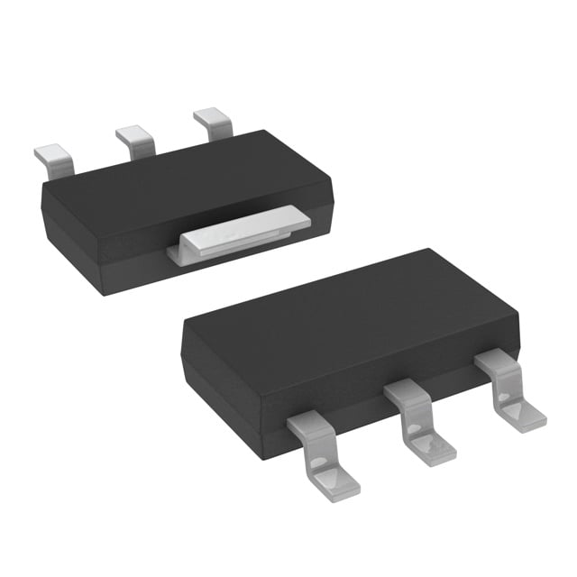
| 描述 | MOSFET N-CH 60V 2.7A SOT223MOSFET N-Chan 60V 2.7 Amp |
| 产品分类 | FET - 单分离式半导体 |
| FET功能 | 逻辑电平门 |
| FET类型 | MOSFET N 通道,金属氧化物 |
| Id-连续漏极电流 | 2.7 A |
| 品牌 | Vishay / SiliconixVishay Siliconix |
| 产品手册 | |
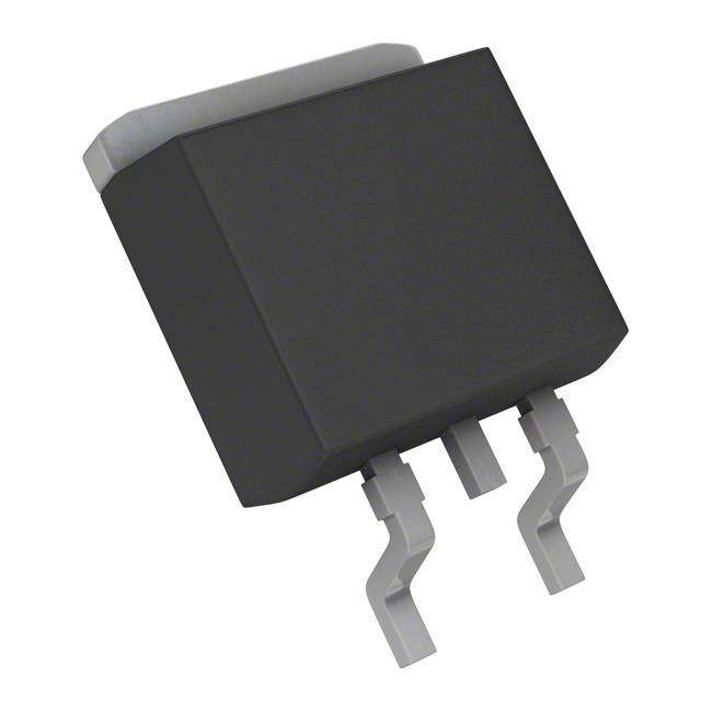
| 产品图片 |
|
| rohs | RoHS 合规性豁免无铅 / 符合限制有害物质指令(RoHS)规范要求 |
| 产品系列 | 晶体管,MOSFET,Vishay / Siliconix IRLL014TRPBF- |
| 数据手册 | |
| 产品型号 | IRLL014TRPBFIRLL014TRPBF |
| Pd-PowerDissipation | 2 W |
| Pd-功率耗散 | 2 W |
| RdsOn-漏源导通电阻 | 200 mOhms |
| Vds-漏源极击穿电压 | 60 V |
| Vgs-Gate-SourceBreakdownVoltage | +/- 10 V |
| Vgs-栅源极击穿电压 | 10 V |
| 上升时间 | 110 ns |
| 下降时间 | 26 ns |
| 不同Id时的Vgs(th)(最大值) | 2V @ 250µA |
| 不同Vds时的输入电容(Ciss) | 400pF @ 25V |
| 不同Vgs时的栅极电荷(Qg) | 8.4nC @ 5V |
| 不同 Id、Vgs时的 RdsOn(最大值) | 200 毫欧 @ 1.6A,5V |
| 产品目录绘图 |
|
| 产品目录页面 | |
| 产品种类 | MOSFET |
| 供应商器件封装 | SOT-223 |
| 其它名称 | *IRLL014TRPBF |
| 典型关闭延迟时间 | 17 ns |
| 功率-最大值 | 2W |
| 功率耗散 | 2 W |
| 包装 | 剪切带 (CT) |
| 商标 | Vishay / Siliconix |
| 安装类型 | 表面贴装 |
| 安装风格 | SMD/SMT |
| 导通电阻 | 200 mOhms |
| 封装 | Reel |
| 封装/外壳 | TO-261-4,TO-261AA |
| 封装/箱体 | SOT-223-3 |
| 工厂包装数量 | 2500 |
| 晶体管极性 | N-Channel |
| 最大工作温度 | + 150 C |
| 最小工作温度 | - 55 C |
| 标准包装 | 1 |
| 汲极/源极击穿电压 | 60 V |
| 漏极连续电流 | 2.7 A |
| 漏源极电压(Vdss) | 60V |
| 电流-连续漏极(Id)(25°C时) | 2.7A (Tc) |
| 通道模式 | Enhancement |
| 配置 | Single Dual Drain |
| 闸/源击穿电压 | +/- 10 V |


- 商务部:美国ITC正式对集成电路等产品启动337调查
- 曝三星4nm工艺存在良率问题 高通将骁龙8 Gen1或转产台积电
- 太阳诱电将投资9.5亿元在常州建新厂生产MLCC 预计2023年完工
- 英特尔发布欧洲新工厂建设计划 深化IDM 2.0 战略
- 台积电先进制程称霸业界 有大客户加持明年业绩稳了
- 达到5530亿美元!SIA预计今年全球半导体销售额将创下新高
- 英特尔拟将自动驾驶子公司Mobileye上市 估值或超500亿美元
- 三星加码芯片和SET,合并消费电子和移动部门,撤换高东真等 CEO
- 三星电子宣布重大人事变动 还合并消费电子和移动部门
- 海关总署:前11个月进口集成电路产品价值2.52万亿元 增长14.8%


PDF Datasheet 数据手册内容提取
IRLL014, SiHLL014 www.vishay.com Vishay Siliconix Power MOSFET FEATURES PRODUCT SUMMARY • Surface mount VDS (V) 60 • Available in tape and reel RDS(on) () VGS = 5.0 V 0.20 • Dynamic dV/dt rating Q max. (nC) 8.4 • Logic-level gate drive g • R specified at V = 4 V and 5 V Q (nC) 3.5 DS(on) GS gs • Fast switching Available Q (nC) 6.0 gd • Ease of paralleling Configuration Single • Material categorization: for definitions of compliance please see www.vishay.com/doc?99912 D DESCRIPTION Third generation power MOSFETs from Vishay provide the SOT-223 designer with the best combination of fast switching, D ruggedized device design, low on-resistance and G cost-effectiveness. S The SOT-223 package is designed for surface-mounting D G using vapor phase, infrared, or wave soldering techniques. Its unique package design allows for easy automatic Marking code: LA S pick-and-place as with other SOT or SOIC packages but has the added advantage of improved thermal performance N-Channel MOSFET due to an enlarged tab for heatsinking. Power dissipation of greater than 1.25 W is possible in a typical surface mount application. ORDERING INFORMATION Package SOT-223 Lead (Pb)-free and Halogen-free SiHLL014TR-GE3 Lead (Pb)-free IRLL014TRPbF a Note a. See device orientation. ABSOLUTE MAXIMUM RATINGS (T = 25 °C, unless otherwise noted) C PARAMETER SYMBOL LIMIT UNIT Drain-Source Voltage V 60 DS V Gate-Source Voltage V ± 10 GS T = 25 °C 2.7 Continuous Drain Current V at 10 V C I GS T = 100 °C D 1.7 A C Pulsed Drain Current a I 22 DM Linear Derating Factor 0.025 W/°C Linear Derating Factor (PCB mount) e 0.017 Single Pulse Avalanche Energy b E 100 mJ AS Repetitive Avalanche Current a I 2.7 A AR Repetitive Avalanche Energy a E 0.31 mJ AR Maximum Power Dissipation T = 25 °C 3.1 C P W Maximum Power Dissipation (PCB mount) e T = 25 °C D 2.0 A Peak Diode Recovery dV/dt c dV/dt 4.5 V/ns Operating Junction and Storage Temperature Range T , T -55 to +150 J stg °C Soldering Recommendations (Peak temperature) d for 10 s 300 Notes a. Repetitive rating; pulse width limited by maximum junction temperature (see fig. 11). b. VDD = 25 V, starting TJ = 25 °C, L = 16 mH, Rg = 25 , IAS = 2.7 A (see fig. 12). c. ISD 10 A, dI/dt 90 A/μs, VDD VDS, TJ 150 °C. d. 1.6 mm from case. e. When mounted on 1" square PCB (FR-4 or G-10 material). S16-0015-Rev. F, 18-Jan-16 1 Document Number: 91319 For technical questions, contact: hvm@vishay.com THIS DOCUMENT IS SUBJECT TO CHANGE WITHOUT NOTICE. THE PRODUCTS DESCRIBED HEREIN AND THIS DOCUMENT ARE SUBJECT TO SPECIFIC DISCLAIMERS, SET FORTH AT www.vishay.com/doc?91000
IRLL014, SiHLL014 www.vishay.com Vishay Siliconix THERMAL RESISTANCE RATINGS PARAMETER SYMBOL MIN. TYP. MAX. UNIT Maximum Junction-to-Ambient R - - 60 (PCB mount) a thJA °C/W Maximum Junction-to-Case (Drain) R - - 40 thJC Note a. When mounted on 1" square PCB (FR-4 or G-10 material). SPECIFICATIONS (T = 25 °C, unless otherwise noted) J PARAMETER SYMBOL TEST CONDITIONS MIN. TYP. MAX. UNIT Static Drain-Source Breakdown Voltage V V = 0 V, I = 250 μA 60 - - V DS GS D VDS Temperature Coefficient VDS/TJ Reference to 25 °C, ID = 1 mA - 0.073 - V/°C Gate-Source Threshold Voltage V V = V , I = 250 μA 1.0 - 2.0 V GS(th) DS GS D Gate-Source Leakage I V = ± 10 V - - ± 100 nA GSS GS V = 60 V, V = 0 V - - 25 DS GS Zero Gate Voltage Drain Current I μA DSS V = 48 V, V = 0 V, T = 125 °C - - 250 DS GS J V = 5.0 V I = 1.6 A b - - 0.20 GS D Drain-Source On-State Resistance RDS(on) V = 4.0 V I = 1.4 A b - - 0.28 GS D Forward Transconductance g V = 25 V, I = 1.6 A 3.2 - - S fs DS D Dynamic Input Capacitance C - 400 - iss V = 0 V, GS Output Capacitance C V = 25 V, - 170 - pF oss DS f = 1.0 MHz, see fig. 5 Reverse Transfer Capacitance C - 42 - rss Total Gate Charge Q - - 8.4 g I = 10 A, V = 48 V, Gate-Source Charge Q V = 5.0 V D DS - - 3.5 nC gs GS see fig. 6 and 13 b Gate-Drain Charge Q - - 6.0 gd Turn-On Delay Time t - 9.3 - d(on) Rise Time tr VDD = 30 V, ID = 10 A, - 110 - ns Turn-Off Delay Time td(off) Rg = 12 , RD = 2.8 , see fig. 10 b - 17 - Fall Time t - 26 - f Internal Drain Inductance L Between lead, D - 4.0 - D 6 mm (0.25") from nH package and center of G Internal Source Inductance LS die contact - 6.0 - S Drain-Source Body Diode Characteristics Continuous Source-Drain Diode Current IS MOSFET symbol D - - 2.7 showing the A integral reverse G Pulsed Diode Forward Current a ISM p - n junction diode S - - 22 Body Diode Voltage V T = 25 °C, I = 2.7 A, V = 0 V b - - 1.6 V SD J S GS Body Diode Reverse Recovery Time t - 65 130 ns rr T = 25 °C, I = 10 A, dI/dt = 100 A/μs b J F Body Diode Reverse Recovery Charge Q - 0.33 0.65 μC rr Forward Turn-On Time t Intrinsic turn-on time is negligible (turn-on is dominated by L and L ) on S D Notes a. Repetitive rating; pulse width limited by maximum junction temperature (see fig. 11). b. Pulse width 300 μs; duty cycle 2 %. S16-0015-Rev. F, 18-Jan-16 2 Document Number: 91319 For technical questions, contact: hvm@vishay.com THIS DOCUMENT IS SUBJECT TO CHANGE WITHOUT NOTICE. THE PRODUCTS DESCRIBED HEREIN AND THIS DOCUMENT ARE SUBJECT TO SPECIFIC DISCLAIMERS, SET FORTH AT www.vishay.com/doc?91000
IRLL014, SiHLL014 www.vishay.com Vishay Siliconix TYPICAL CHARACTERISTICS (25 °C, unless otherwise noted) 101TopV7543G....S5005 VVVV sistance 32..05 IVDG =S 1=0 1 A0 V 3.0 V e ent (A) 10B0ottom2.27.55 VV e On Red) 2.0 Curr ourcmaliz 1.5 Drain 10-1 n-to-S(Nor 1.0 I, D 2.25 V Drai 10-2 20 µs Pulse Width , on) 0.5 TC = 25 °C RDS( 0.0 10-1 100 101 - 60- 40- 20 0 20 40 60 80 100120 140 160 VDS, Drain-to-Source Voltage (V) TJ, Junction Temperature (°C) Fig. 1 - Typical Output Characteristics, T = 25 °C Fig. 4 - Normalized On-Resistance vs. Temperature C TopV7G.S5V 700 VGS = 0 V, f = 1 MHz 5.0V C = C + C , C Shorted 101 43..05VV 600 Ciss = Cgs gd ds 3.0V rss gd Current (A) 10B0ottom22.7.55VV ance (pF) 450000 Coss = Cds C+i sCsgd Drain 10-1 2.25 V apacit 300 Coss , D C 200 I 10-2 20µs PulseWidth 100 Crss T = 150 °C C 0 10-1 100 101 100 101 VDS, Drain-to-SourceVoltage (V) VDS, Drain-to-Source Voltage (V) Fig. 2 - Typical Output Characteristics, T = 150 °C Fig. 5 - Typical Capacitance vs. Drain-to-Source Voltage C 101 10 I = 10 A D V) 150 °C ge ( 6 ent (A) 100 e Volta 6 VDS =V 3D0S V= 48 V Curr 10-1 25 °C ourc n S ai o- 4 Dr e-t , D 10-2 at I G , S 2 20 µs Pulse Width VG For test circuit 10-3 VDS = 25 V see figure 13 0 2 2.5 3 3.5 4 4.5 5 0 2 4 6 8 10 VGS, Gate-to-Source Voltage (V) QG, Total Gate Charge (nC) Fig. 3 - Typical Transfer Characteristics Fig. 6 - Typical Gate Charge vs. Gate-to-Source Voltage S16-0015-Rev. F, 18-Jan-16 3 Document Number: 91319 For technical questions, contact: hvm@vishay.com THIS DOCUMENT IS SUBJECT TO CHANGE WITHOUT NOTICE. THE PRODUCTS DESCRIBED HEREIN AND THIS DOCUMENT ARE SUBJECT TO SPECIFIC DISCLAIMERS, SET FORTH AT www.vishay.com/doc?91000
IRLL014, SiHLL014 www.vishay.com Vishay Siliconix R D V A) TJ = 150 °C DS nt ( 101 VGS D.U.T. e urr Rg + C -VDD n ai Dr T = 25 °C 10 V e 100 J Pulse width ≤ 1 µs ers Duty factor ≤ 0.1 % v e R , D Fig. 10a - Switching Time Test Circuit S I V = 0 V GS 10-1 V 0.4 0.8 1.2 1.6 2.0 2.4 DS 90 % V , Source-to-Drain Voltage (V) SD Fig. 7 - Typical Source-Drain Diode Forward Voltage 10 % V GS 103 t t t t d(on) r d(off) f 5 Fig. 10b - Switching Time Waveforms 2 Operation in this area limited by R A) 102 DS(on) nt ( 5 e 2 urr 10 C 100 µs n 5 ai 1 ms Dr 2 , D 1 10 ms I 5 TC = 25 °C 2 TJ = 150 °C Single Pulse 0.1 0.1 2 5 1 2 5 10 2 5 102 2 5 103 V , Drain-to-Source Voltage (V) DS Fig. 8 - Maximum Safe Operating Area 3.0 2.5 A) nt ( 2.0 e Curr 1.5 n ai Dr 1.0 , D I 0.5 0.0 25 50 75 100 125 150 T , Case Temperature (°C) C Fig. 9 - Maximum Drain Current vs. Case Temperature S16-0015-Rev. F, 18-Jan-16 4 Document Number: 91319 For technical questions, contact: hvm@vishay.com THIS DOCUMENT IS SUBJECT TO CHANGE WITHOUT NOTICE. THE PRODUCTS DESCRIBED HEREIN AND THIS DOCUMENT ARE SUBJECT TO SPECIFIC DISCLAIMERS, SET FORTH AT www.vishay.com/doc?91000
IRLL014, SiHLL014 www.vishay.com Vishay Siliconix 102 )C D = 0.50 ZthJ 10 0.20 e ( 0.10 s n 0.05 o sp 1 0.02 PDM e R 0.01 mal Single Pulse t1 er 10-1 (Thermal Response) t2 h T Notes: 1. Duty Factor, D = t/t 1 2 2. Peak T = P x Z + T j DM thJC C 10-2 10-5 10-4 10-3 10-2 0.1 1 101 102 103 t , Rectangular Pulse Duration (s) 1 Fig. 11 - Maximum Effective Transient Thermal Impedance, Junction-to-Case L V V DS DS Vary tp to obtain tp required I AS V DD Rg D.U.T + V - DD V DS I AS 10 V t 0.01 Ω p I AS Fig. 12a - Unclamped Inductive Test Circuit Fig. 12b - Unclamped Inductive Waveforms mJ) 250 gy ( Top 1.I2D A er 200 1.7 A En Bottom 2.7 A e h c an 150 al v A e 100 s ul P e gl 50 n Si , AS 0 VDD = 25 V E 25 50 75 100 125 150 Starting T, Junction Temperature (°C) J Fig. 12c - Maximum Avalanche Energy vs. Drain Current S16-0015-Rev. F, 18-Jan-16 5 Document Number: 91319 For technical questions, contact: hvm@vishay.com THIS DOCUMENT IS SUBJECT TO CHANGE WITHOUT NOTICE. THE PRODUCTS DESCRIBED HEREIN AND THIS DOCUMENT ARE SUBJECT TO SPECIFIC DISCLAIMERS, SET FORTH AT www.vishay.com/doc?91000
IRLL014, SiHLL014 www.vishay.com Vishay Siliconix Current regulator Same type as D.U.T. Q 50 kΩ G VGS 12 V 0.2 µF 0.3 µF QGS QGD + V D.U.T. - DS V G V GS 3 mA Charge I I G D Current sampling resistors Fig. 13a - Basic Gate Charge Waveform Fig. 13b - Gate Charge Test Circuit Peak Diode Recovery dV/dt Test Circuit + Circuit layout considerations D.U.T. • Low stray inductance • Ground plane • Low leakage inductance current transformer - + - + - Rg • dV/dt controlled by Rg + •• DISrDi vceorn staromlleed t ybpye d aust yD f.aUc.Tto.r “D” -VDD • D.U.T. - device under test Driver gate drive Period D = P.W. P.W. Period VGS = 10 Va D.U.T. lSD waveform Reverse recovery Body diode forward current current dI/dt D.U.T. VDS waveform Diode recovery dV/dt VDD Re-applied voltage Body diode forward drop Inductor current Ripple ≤ 5 % ISD Note a. VGS = 5 V for logic level devices Fig. 14 - For N-Channel Vishay Siliconix maintains worldwide manufacturing capability. Products may be manufactured at one of several qualified locations. Reliability data for Silicon Technology and Package Reliability represent a composite of all qualified locations. For related documents such as package/tape drawings, part marking, and reliability data, see www.vishay.com/ppg?91319. S16-0015-Rev. F, 18-Jan-16 6 Document Number: 91319 For technical questions, contact: hvm@vishay.com THIS DOCUMENT IS SUBJECT TO CHANGE WITHOUT NOTICE. THE PRODUCTS DESCRIBED HEREIN AND THIS DOCUMENT ARE SUBJECT TO SPECIFIC DISCLAIMERS, SET FORTH AT www.vishay.com/doc?91000
Package Information Vishay Siliconix SOT-223 (HIGH VOLTAGE) D B A 3 0.08 (0.003) B1 C 00..1100 ((00..000044))MMCC BMM A 4 3 H E 0.20 (0.008)MC AM L1 1 2 3 4 x L 3 x B e θ 0.10 (0.004)MC BM e1 4 x C MILLIMETERS INCHES DIM. MIN. MAX. MIN. MAX. A 1.55 1.80 0.061 0.071 B 0.65 0.85 0.026 0.033 B1 2.95 3.15 0.116 0.124 C 0.25 0.35 0.010 0.014 D 6.30 6.70 0.248 0.264 E 3.30 3.70 0.130 0.146 e 2.30 BSC 0.0905 BSC e1 4.60 BSC 0.181 BSC H 6.71 7.29 0.264 0.287 L 0.91 - 0.036 - L1 0.061 BSC 0.0024 BSC θ - 10' - 10' ECN: S-82109-Rev. A, 15-Sep-08 DWG: 5969 Notes 1. Dimensioning and tolerancing per ASME Y14.5M-1994. 2. Dimensions are shown in millimeters (inches). 3. Dimension do not include mold flash. 4. Outline conforms to JEDEC outline TO-261AA. Document Number: 91363 www.vishay.com Revision: 15-Sep-08 1
Legal Disclaimer Notice www.vishay.com Vishay Disclaimer ALL PRODUCT, PRODUCT SPECIFICATIONS AND DATA ARE SUBJECT TO CHANGE WITHOUT NOTICE TO IMPROVE RELIABILITY, FUNCTION OR DESIGN OR OTHERWISE. Vishay Intertechnology, Inc., its affiliates, agents, and employees, and all persons acting on its or their behalf (collectively, “Vishay”), disclaim any and all liability for any errors, inaccuracies or incompleteness contained in any datasheet or in any other disclosure relating to any product. Vishay makes no warranty, representation or guarantee regarding the suitability of the products for any particular purpose or the continuing production of any product. To the maximum extent permitted by applicable law, Vishay disclaims (i) any and all liability arising out of the application or use of any product, (ii) any and all liability, including without limitation special, consequential or incidental damages, and (iii) any and all implied warranties, including warranties of fitness for particular purpose, non-infringement and merchantability. Statements regarding the suitability of products for certain types of applications are based on Vishay’s knowledge of typical requirements that are often placed on Vishay products in generic applications. Such statements are not binding statements about the suitability of products for a particular application. It is the customer’s responsibility to validate that a particular product with the properties described in the product specification is suitable for use in a particular application. Parameters provided in datasheets and / or specifications may vary in different applications and performance may vary over time. All operating parameters, including typical parameters, must be validated for each customer application by the customer’s technical experts. Product specifications do not expand or otherwise modify Vishay’s terms and conditions of purchase, including but not limited to the warranty expressed therein. Except as expressly indicated in writing, Vishay products are not designed for use in medical, life-saving, or life-sustaining applications or for any other application in which the failure of the Vishay product could result in personal injury or death. Customers using or selling Vishay products not expressly indicated for use in such applications do so at their own risk. Please contact authorized Vishay personnel to obtain written terms and conditions regarding products designed for such applications. No license, express or implied, by estoppel or otherwise, to any intellectual property rights is granted by this document or by any conduct of Vishay. Product names and markings noted herein may be trademarks of their respective owners. © 2017 VISHAY INTERTECHNOLOGY, INC. ALL RIGHTS RESERVED Revision: 08-Feb-17 1 Document Number: 91000
Mouser Electronics Authorized Distributor Click to View Pricing, Inventory, Delivery & Lifecycle Information: V ishay: IRLL014TRPBF IRLL014 IRLL014TR IRLL014PBF