ICGOO在线商城 > 分立半导体产品 > 晶体管 - FET,MOSFET - 单 > FDS6675BZ
/FDS6675BZ.jpg)
 Datasheet下载
- 型号: FDS6675BZ
- 制造商: Fairchild Semiconductor
- 库位|库存: xxxx|xxxx
- 要求:
| 数量阶梯 | 香港交货 | 国内含税 |
| +xxxx | $xxxx | ¥xxxx |
查看当月历史价格
查看今年历史价格
FDS6675BZ产品简介:
ICGOO电子元器件商城为您提供FDS6675BZ由Fairchild Semiconductor设计生产,在icgoo商城现货销售,并且可以通过原厂、代理商等渠道进行代购。 FDS6675BZ价格参考¥2.97-¥3.71。Fairchild SemiconductorFDS6675BZ封装/规格:晶体管 - FET,MOSFET - 单, 表面贴装 P 沟道 30V 11A(Ta) 2.5W(Ta) 8-SO。您可以下载FDS6675BZ参考资料、Datasheet数据手册功能说明书,资料中有FDS6675BZ 详细功能的应用电路图电压和使用方法及教程。
FDS6675BZ是ON Semiconductor(安森美半导体)生产的单个MOSFET晶体管,具体应用场景包括但不限于以下几个方面:

1. 电源管理:FDS6675BZ适用于各种电源管理系统,例如开关电源、DC-DC转换器等。其低导通电阻(Rds(on))特性使其在高频开关应用中表现出色,能够有效降低功率损耗,提高效率。

2. 电机驱动:该器件可以用于驱动小型直流电机或步进电机,特别是在需要高精度控制和快速响应的应用中。其较低的栅极电荷(Qg)有助于实现更高效的开关操作,减少能量损失。

3. 负载切换:FDS6675BZ可用于实现负载切换功能,如USB端口保护、电池充电电路中的电流路径控制等。它能够快速可靠地切断或接通电流,确保系统的安全性和稳定性。

4. LED驱动:对于LED照明系统,此MOSFET可以用作恒流源控制器的一部分,通过PWM调光等方式精确调节LED亮度,同时保持良好的散热性能。

5. 通信设备:在网络路由器、交换机等通信产品内部,FDS6675BZ可作为信号调理元件,帮助处理数据传输过程中的电压水平转换等问题。

6. 消费电子产品:在智能手机、平板电脑等便携式电子设备中,这款MOSFET常被用来优化电源管理单元的设计,延长电池寿命并提升用户体验。

总之,FDS6675BZ凭借其优异的电气参数和可靠性,在众多领域都有着广泛的应用前景。用户可以根据实际需求选择合适的工作条件来发挥其最佳性能。
| 参数 | 数值 |
| 产品目录 | |
| ChannelMode | Enhancement |
| 描述 | MOSFET P-CH 30V 8-SOICMOSFET -30V P-Channel PwrTrch MOSFET |
| 产品分类 | FET - 单分离式半导体 |
| FET功能 | 逻辑电平门 |
| FET类型 | MOSFET P 通道,金属氧化物 |
| Id-ContinuousDrainCurrent | 11 A |
| Id-连续漏极电流 | 11 A |
| 品牌 | Fairchild Semiconductor |
| 产品手册 | |
| 产品图片 |
|
| rohs | 符合RoHS无铅 / 符合限制有害物质指令(RoHS)规范要求 |
| 产品系列 | 晶体管,MOSFET,Fairchild Semiconductor FDS6675BZPowerTrench® |
| 数据手册 | |
| 产品型号 | FDS6675BZ |
| PCN组件/产地 | |
| PCN设计/规格 | |
| Pd-PowerDissipation | 2.5 W |
| Pd-功率耗散 | 2.5 W |
| RdsOn-Drain-SourceResistance | 10.8 mOhms |
| RdsOn-漏源导通电阻 | 10.8 mOhms |
| Vds-Drain-SourceBreakdownVoltage | - 30 V |
| Vds-漏源极击穿电压 | - 30 V |
| Vgs-Gate-SourceBreakdownVoltage | +/- 25 V |
| Vgs-栅源极击穿电压 | 25 V |
| 上升时间 | 7.8 ns |
| 下降时间 | 60 ns |
| 不同Id时的Vgs(th)(最大值) | 3V @ 250µA |
| 不同Vds时的输入电容(Ciss) | 2470pF @ 15V |
| 不同Vgs时的栅极电荷(Qg) | 62nC @ 10V |
| 不同 Id、Vgs时的 RdsOn(最大值) | 13 毫欧 @ 11A,10V |
| 产品目录页面 | |
| 产品种类 | MOSFET |
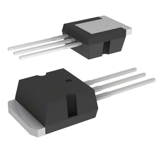
| 供应商器件封装 | 8-SO |
| 其它名称 | FDS6675BZDKR |
| 典型关闭延迟时间 | 120 ns |
| 功率-最大值 | 1W |
| 包装 | Digi-Reel® |
| 单位重量 | 187 mg |
| 商标 | Fairchild Semiconductor |
| 安装类型 | 表面贴装 |
| 安装风格 | SMD/SMT |
| 封装 | Reel |
| 封装/外壳 | 8-SOIC(0.154",3.90mm 宽) |
| 封装/箱体 | SOIC-8 Narrow |
| 工厂包装数量 | 2500 |
| 晶体管极性 | P-Channel |
| 最大工作温度 | + 150 C |
| 最小工作温度 | - 55 C |
| 标准包装 | 1 |
| 正向跨导-最小值 | 34 S |
| 漏源极电压(Vdss) | 30V |
| 电流-连续漏极(Id)(25°C时) | 11A (Ta) |
| 系列 | FDS6675 |
| 通道模式 | Enhancement |
| 配置 | Single Quad Drain Triple Source |


- 商务部:美国ITC正式对集成电路等产品启动337调查
- 曝三星4nm工艺存在良率问题 高通将骁龙8 Gen1或转产台积电
- 太阳诱电将投资9.5亿元在常州建新厂生产MLCC 预计2023年完工
- 英特尔发布欧洲新工厂建设计划 深化IDM 2.0 战略
- 台积电先进制程称霸业界 有大客户加持明年业绩稳了
- 达到5530亿美元!SIA预计今年全球半导体销售额将创下新高
- 英特尔拟将自动驾驶子公司Mobileye上市 估值或超500亿美元
- 三星加码芯片和SET,合并消费电子和移动部门,撤换高东真等 CEO
- 三星电子宣布重大人事变动 还合并消费电子和移动部门
- 海关总署:前11个月进口集成电路产品价值2.52万亿元 增长14.8%


PDF Datasheet 数据手册内容提取
Is Now Part of To learn more about ON Semiconductor, please visit our website at www.onsemi.com Please note: As part of the Fairchild Semiconductor integration, some of the Fairchild orderable part numbers will need to change in order to meet ON Semiconductor’s system requirements. Since the ON Semiconductor product management systems do not have the ability to manage part nomenclature that utilizes an underscore (_), the underscore (_) in the Fairchild part numbers will be changed to a dash (-). This document may contain device numbers with an underscore (_). Please check the ON Semiconductor website to verify the updated device numbers. The most current and up-to-date ordering information can be found at www.onsemi.com. Please email any questions regarding the system integration to Fairchild_questions@onsemi.com. ON Semiconductor and the ON Semiconductor logo are trademarks of Semiconductor Components Industries, LLC dba ON Semiconductor or its subsidiaries in the United States and/or other countries. ON Semiconductor owns the rights to a number of patents, trademarks, copyrights, trade secrets, and other intellectual property. A listing of ON Semiconductor’s product/patent coverage may be accessed at www.onsemi.com/site/pdf/Patent-Marking.pdf. ON Semiconductor reserves the right to make changes without further notice to any products herein. ON Semiconductor makes no warranty, representation or guarantee regarding the suitability of its products for any particular purpose, nor does ON Semiconductor assume any liability arising out of the application or use of any product or circuit, and specifically disclaims any and all liability, including without limitation special, consequential or incidental damages. Buyer is responsible for its products and applications using ON Semiconductor products, including compliance with all laws, regulations and safety requirements or standards, regardless of any support or applications information provided by ON Semiconductor. “Typical” parameters which may be provided in ON Semiconductor data sheets and/or specifications can and do vary in different applications and actual performance may vary over time. All operating parameters, including “Typicals” must be validated for each customer application by customer’s technical experts. ON Semiconductor does not convey any license under its patent rights nor the rights of others. ON Semiconductor products are not designed, intended, or authorized for use as a critical component in life support systems or any FDA Class 3 medical devices or medical devices with a same or similar classification in a foreign jurisdiction or any devices intended for implantation in the human body. Should Buyer purchase or use ON Semiconductor products for any such unintended or unauthorized application, Buyer shall indemnify and hold ON Semiconductor and its officers, employees, subsidiaries, affiliates, and distributors harmless against all claims, costs, damages, and expenses, and reasonable attorney fees arising out of, directly or indirectly, any claim of personal injury or death associated with such unintended or unauthorized use, even if such claim alleges that ON Semiconductor was negligent regarding the design or manufacture of the part. ON Semiconductor is an Equal Opportunity/Affirmative Action Employer. This literature is subject to all applicable copyright laws and is not for resale in any manner.
F D S 6 6 March 2009 7 FDS6675BZ 5 B P-Channel PowerTrench® MOSFET Z tm P -30V, -11A, 13mΩ - C h General Description Features a n This P-Channel MOSFET is producted using Fairchild (cid:132) Max rDS(on) = 13mΩ at VGS = -10V, ID = -11A n Semiconductor’s advanced PowerTrench process that has e been especially tailored to minimize the on-state (cid:132) Max rDS(on) = 21.8mΩ at VGS = -4.5V, ID = -9A l P resistance. (cid:132) Extended V range (-25V) for battery applications o GS This device is well suited for Power Management and load w switching applications common in Notebook Computers (cid:132) HBM ESD protection level of 5.4 KV typical (note 3) e r and Portable Battery Packs. (cid:132) High performance trench technology for extremely low T rDS(on) re n (cid:132) High power and current handing capability c h (cid:132) RoHS Compliant ® M O S D F D 5 4 E D T D 6 3 7 2 G S S 8 1 SO-8 S MOSFET Maximum Ratings TA = 25°C unless otherwise noted Symbol Parameter Ratings Units V Drain to Source Voltage -30 V DS V Gate to Source Voltage ±25 V GS Drain Current -Continuous (Note 1a) -11 I A D -Pulsed -55 Power Dissipation for Single Operation (Note 1a) 2.5 P (Note 1b) 1.2 W D (Note 1c) 1.0 T , T Operating and Storage Temperature -55 to 150 °C J STG Thermal Characteristics R Thermal Resistance , Junction to Ambient (Note 1a) 50 °C/W θJA R Thermal Resistance , Junction to Case (Note 1) 25 °C/W θJC Package Marking and Ordering Information Device Marking Device Reel Size Tape Width Quantity FDS6675BZ FDS6675BZ 13’’ 12mm 2500 units ©2009 Fairchild Semiconductor Corporation 1 www.fairchildsemi.com FDS6675BZ Rev. B2
Electrical Characteristics F TJ = 25°C unless otherwise noted D S Symbol Parameter Test Conditions Min Typ Max Units 6 Off Characteristics 6 7 B Drain to Source Breakdown Voltage I = -250µA, V = 0V -30 V 5 VDSS D GS B ∆B Breakdown Voltage Temperature I = -250µA, referenced to VDSS D -20 mV/°C Z ∆TJ Coefficient 25°C P I Zero Gate Voltage Drain Current V = -24V, V = 0V -1 µA DSS DS GS - C I Gate to Source Leakage Current V = ±25V, V = 0V ±10 µA GSS GS DS h a On Characteristics (Note 2) n V Gate to Source Threshold Voltage V = V , I = -250µA -1 -2 -3 V n GS(th) GS DS D e ∆VGS(th) Gate to Source Threshold Voltage ID = -250µA, referenced to 15.7 mV/°C l ∆T Temperature Coefficient 25°C P J V = -10V , I = -11A 10.8 13.0 o GS D w V = -4.5V, I = -9A 17.4 21.8 r Drain to Source On Resistance GS D mΩ e DS(on) V = -10V, I = -11A r TG =S 125oC D 15.0 18.8 T J r g Forward Transconductance V = -5V, I = -11A 34 S e FS DS D n c Dynamic Characteristics h ® C Input Capacitance 1855 2470 pF Ciss Output Capacitance VDS = -15V, VGS = 0V, 335 450 pF M oss f = 1MHz O C Reverse Transfer Capacitance 330 500 pF rss S Switching Characteristics (Note 2) F E t Turn-On Delay Time 3.0 10 ns T d(on) V = -15V, I = -11A t Rise Time DD D 7.8 16 ns r V = -10V, R = 6Ω t Turn-Off Delay Time GS GS 120 200 ns d(off) t Fall Time 60 100 ns f V = -15V, V = -10V, Q Total Gate Charge DS GS 44 62 nC g I = -11A D Q Total Gate Charge 25 35 nC g V = -15V, V = -5V, Q Gate to Source Gate Charge DS GS 7.2 nC gs I = -11A D Q Gate to Drain Charge 11.4 nC gd Drain-Source Diode Characteristics V Source to Drain Diode Forward Voltage V = 0V, I = -2.1A -0.7 -1.2 V SD GS S t Reverse Recovery Time I = -11A, di/dt = 100A/µs 42 ns rr F Q Reverse Recovery Charge I = -11A, di/dt = 100A/µs 30 nC rr F Notes: 1: RθJA is the sum of the junction-to-case and case-to-ambient thermal resistance where the case thermal reference is defined as the solder mounting surface of the drain pins. RθJC is guaranteed by design while RθCA is determined by the user’s board design. a) 50°C/W when b)105°C/W when c) 125°C/W when mounted on a 1 in2 mounted on a .04 in2 m ounted on a pad of 2 oz copper minimun pad pad of 2 oz copper Scale 1 : 1 on letter size paper 2: Pulse Test:Pulse Width <300 us, Duty Cycle < 2.0% 3: The diode connected between the gate and source serves only as protection against ESD. No gate overvoltage rating is implied. ©2009 Fairchild Semiconductor Corporation 2 www.fairchildsemi.com FDS6675BZ Rev.B2
F Typical Characteristics T = 25°C unless otherwise noted D J S 6 6 60 E 4.0 7 50 VGS = - 10V PDUULTSYE C DYUCRLEA T=I O0.N5 %= M80AµXs TANC 3.5 VGS = - 3.5V PDUULTSYE C DYUCRLEA T=I O0.N5 %= M80AµXs 5B URRENT (A) 3400 VGSV =G S- 4=. 5-V 5V VGS = - 4V ALIZEDE ON-RESIS 23..50 VGS = - 4V VGS = - 4.5V Z P-Ch -I, DRAIN CD 1200 VGS = - 3.5V VGS = - 3V NORMAIN TO SOURC 112...050 VGS V=G -S 1 =0 V- 5V annel P 0 DR 0.5 o 0 1 2 3 4 0 10 20 30 40 50 60 w -VDS, DRAIN TO SOURCE VOLTAGE (V) -ID, DRAIN CURRENT(A) e r T Figure 1. On Region Characteristics Figure 2. Normalized On-Resistance vs Drain r Current and Gate Voltage e n c h E 1.6 50 ® NC ID = -11A ID = -11A PULSE DURATION = 80µs M NORMALIZEDN TO SOURCE ON-RESISTA 0111....8024 VGS = -10V r, DRAIN TO SOURCE DS(on)ON-RESISTANCE m()Ω 12340000 DUTTYJ CT=J Y2 =C5 o1LC5E0 o=C 0.5%MAX OSFET AI DR 0.6-80 -40 0 40 80 120 160 03.0 4.5 6.0 7.5 9.0 10 TJ, JUNCTION TEM PERATURE (oC) -VGS, GATE TO SOURCE VOLTAGE (V) Figure 3. Normalized On Resistance vs Junction Figure 4. On-Resistance vs Gate to Source Temperature Voltage 60 100 NT (A) 50 PDUULTSYE C DYUCRLEA T=I O0.N5 %= M80AµXs RENT (A) 10 VGS = 0V RE 40 UR TJ = 150oC R C 1 U N DRAIN C 2300 TJ = 150oC SE DRAI 0.1 TJ = 25oC -I, D10 TJ = 25oC EVER 0.01 TJ = -55oC R 0 TJ = -55oC -I, S1E-3 2.0 2.5 3.0 3.5 4.0 4.5 0.0 0.2 0.4 0.6 0.8 1.0 1.2 1.4 -VGS, GATE TO SOURCE VOLTAGE (V) -VSD, BODY DIODE FORWARD VOLTAGE (V) Figure 5. Transfer Characteristics Figure 6. Source to Drain Diode Forward Voltage vs Source Current ©2009 Fairchild Semiconductor Corporation 3 www.fairchildsemi.com FDS6675BZ Rev.B2
F Typical Characteristics T = 25°C unless otherwise noted D J S 6 6 10 4000 V) 7 GE( Ciss 5B A 8 T F) Z L p RCE VO 6 VDD = -10V VDD = -15V ANCE ( 1000 Coss P-C OU CIT h E TO S 4 VDD = -20V CAPA Crss ann , GATS 2 fV =GS 1 =M 0HVz el P VG 0 100 o - 0 10 20 30 40 50 0.1 1 10 30 w Qg, GATE CHARGE(nC) -VDS, DRAIN TO SOURCE VOLTAGE (V) e r T Figure 7. Gate Charge Characteristics Figure 8. Capacitance vs Drain to Source Voltage r e n c 1000 A) 20 h T( ® 100 N RE 10 M 10 TJ = 150oC UR O uA) 1 HE C TJ = 25oC SF -I(g 0.1 ANC ET 0.01 TJ = 25oC VAL TJ = 125oC A , S 1E-3 -IA 1E-4 1 0 5 10 15 20 25 30 35 10-2 10-1 100 101 102 -VGS(V) tAV, TIME IN AVALANCHE(ms) Figure 9. I vs V Figure 10. Unclamped Inductive Switching g GS Capability 12 100 100 us 10 A) NT ( 8 VGS = -10V T (A) 10 1 ms E N R E R R 10 ms RAIN CU 46 VGS = -4.5V RAIN CUR 1 TLSIHIMNISIGT LAEERD E PBAUY LI SrSD ES(on) 110 s0 ms -I, DD 2 I, DD 0.1 TRJθ J=A M= A1X2 5R oACT/WED 1D0C s TA = 25 oC 0 0.01 25 50 75 100 125 150 0.01 0.1 1 10 100200 TA, AMBIENT TEMPERATURE(oC) VDS, DRAIN to SOU RCE VOLTAGE (V) Figure 11. Maximum Continuous Drain Current vs Figure 12. Forward Bias Safe Operating Area Ambient Temperature ©2009 Fairchild Semiconductor Corporation 4 www.fairchildsemi.com FDS6675BZ Rev.B2
F Typical Characteristics T = 25°C unless otherwise noted D J S 6 6 104 7 W) 5B ER ( 103 VGS = -10 V Z W O P P ENT 102 -C SI h AN a R SINGLE PULSE n T PEAK 10 RTAθJ =A 2=5 1 o2C5 oC/W nel , )PK 1 P P( 0.5 o 10-4 10-3 10-2 10-1 1 10 102 103 w t, PULSE WIDTH (sec) e r T Figure 13. Single Pulse Maximum Power Dissipation r e n c h 2 ® 1 DUTY CYCLE-DESCENDING ORDER M O L D = 0.5 MA A10-1 0.2 S LIZED THER EDANCE,ZJθ10-2 0000....1000521 PDM t1 FET MAMP SINGLE PULSE t2 NORI10-3 RθJA = 125 oC/W NDOUTTYE SF:ACTOR: D = t1/t2 PEAK TJ = PDM x ZθJA x RθJA + TA 10-4 10-4 10-3 10-2 10-1 1 10 102 103 t, RECTANGULAR PULSE DURATION (sec) Figure 14. Junction-to-Ambient Transient Thermal Response Curve ©2009 Fairchild Semiconductor Corporation 5 www.fairchildsemi.com FDS6675BZ Rev.B2
F D S 6 6 7 5 B Z TRADEMARKS The following includes registered and unregistered trademarks and service marks, owned by Fairchild Semiconductor and/or its global subsidiaries, and is not P intended to be an exhaustive list of all such trademarks. - C Build it Now™ FRFET® Programmable Active Droop™ h CorePLUS™ Global Power ResourceSM QFET® a CorePOWER™ Green FPS™ QS™ TinyBoost™tm n CROSSVOLT™ Green FPS™ e-Series™ Quiet Series™ TinyBuck™ n CTL™ GTO™ RapidConfigure™ TinyLogic® e CEcuorrSePntA TRrKan®sfer Logic™ IISntOelPliMLAANXA™R™ ™ TTIinNyYPOoPwTeOr™™ l P EfficentMax™ MegaBuck™ Saving our world, 1mW /W /kW at a time™ TinyPWM™ o EZSWITCH™ * MICROCOUPLER™ SmartMax™ ™ MicroFET™ SMART START™ TinyWire™ w MicroPak™ SPM® TriFault Detect™ e ® MillerDrive™ STEALTH™ TµSReUrEDCesU™RRENT™* rT MotionMax™ SuperFET™ Fairctmhild® Motion-SPM™ SuperSOT™-3 re Fairchild Semiconductor® OPTOLOGIC® SuperSOT™-6 n FFFAAASCCTTT®® Quiet Series™ OPTO®PLANAR® SSSyuunppcreeFrMSEOTO™TS™™-8 UUlHtrCa ®FRFET™ ch® FFalassthvWCorirtee™r® * PDPtm SPM™ ® UVCniXF™ET™ M FF-PPSF™S™ PPoowweerrT-SrePnMc™h® The Power Franchise® VXiSs™ualMax™ O PowerXS™ S *Trademarks of System General Corporation, used under license by Fairchild Semiconductor. F E DISCLAIMER T FAIRCHILD SEMICONDUCTOR RESERVES THE RIGHT TO MAKE CHANGES WITHOUT FURTHER NOTICE TO ANY PRODUCTS HEREIN TO IMPROVE RELIABILITY, FUNCTION, OR DESIGN. FAIRCHILD DOES NOT ASSUME ANY LIABILITY ARISING OUT OF THE APPLICATION OR USE OF ANY PRODUCT OR CIRCUIT DESCRIBED HEREIN; NEITHER DOES IT CONVEY ANY LICENSE UNDER ITS PATENT RIGHTS, NOR THE RIGHTS OF OTHERS. THESE SPECIFICATIONS DO NOT EXPAND THE TERMS OF FAIRCHILD’S WORLDWIDE TERMS AND CONDITIONS, SPECIFICALLY THE WARRANTY THEREIN, WHICH COVERS THESE PRODUCTS. LIFE SUPPORT POLICY FAIRCHILD’S PRODUCTS ARE NOT AUTHORIZED FOR USE AS CRITICAL COMPONENTS IN LIFE SUPPORT DEVICES OR SYSTEMS WITHOUT THE EXPRESS WRITTEN APPROVAL OF FAIRCHILD SEMICONDUCTOR CORPORATION. As used herein: 1. Life support devices or systems are devices or systems which, (a) are 2. A critical component in any component of a life support, device, or intended for surgical implant into the body or (b) support or sustain life, system whose failure to perform can be reasonably expected to cause and (c) whose failure to perform when properly used in accordance with the failure of the life support device or system, or to affect its safety or instructions for use provided in the labeling, can be reasonably effectiveness. expected to result in a significant injury of the user. ANTI-COUNTERFEITING POLICY Fairchild Semiconductor Corporation’s Anti-Counterfeiting Policy. Fairchild’s Anti-Counterfeiting Policy is also stated on our external website, www.Fairchildsemi.com, under Sales Support. Counterfeiting of semiconductor parts is a growing problem in the industry. All manufactures of semiconductor products are experiencing counterfeiting of their parts. Customers who inadvertently purchase counterfeit parts experience many problems such as loss of brand reputation, substandard performance, failed application, and increased cost of production and manufacturing delays. Fairchild is taking strong measures to protect ourselves and our customers from the proliferation of counterfeit parts. Fairchild strongly encourages customers to purchase Fairchild parts either directly from Fairchild or from Authorized Fairchild Distributors who are listed by country on our web page cited above. Products customers buy either from fairchild directly or from Authorized Fairchild Distributors are genuine parts, have full traceability, meet Fairchild’s quality standards for handing and storage and provide access to Fairchild’s full range of up-to-date technical and product information. Fairchild and our Authorized Distributors will stand behind all warranties and will appropriately address and warranty issues that may arise. Fairchild will not provide any warranty coverage or other assistance for parts bought from Unauthorized Sources. Fairchild is committed to combat this global problem and encourage our customers to do their part in stopping this practice by buying direct or from authorized distributors. PRODUCT STATUS DEFINITIONS Definition of Terms Datasheet Identification Product Status Definition Datasheet contains the design specifications for product development. Specifications Advance Information Formative / In Design may change in any manner without notice. Datasheet contains preliminary data; supplementary data will be published at a later Preliminary First Production date. Fairchild Semiconductor reserves the right to make changes at any time without notice to improve design. Datasheet contains final specifications. Fairchild Semiconductor reserves the right to No Identification Needed Full Production make changes at any time without notice to improve the design. Datasheet contains specifications on a product that is discontinued by Fairchild Obsolete Not In Production Semiconductor. The datasheet is for reference information only. Rev. I39 ©2009 Fairchild Semiconductor Corporation 6 www.fairchildsemi.com FDS6675BZ Rev.B2
ON Semiconductor and are trademarks of Semiconductor Components Industries, LLC dba ON Semiconductor or its subsidiaries in the United States and/or other countries. ON Semiconductor owns the rights to a number of patents, trademarks, copyrights, trade secrets, and other intellectual property. A listing of ON Semiconductor’s product/patent coverage may be accessed at www.onsemi.com/site/pdf/Patent−Marking.pdf. ON Semiconductor reserves the right to make changes without further notice to any products herein. ON Semiconductor makes no warranty, representation or guarantee regarding the suitability of its products for any particular purpose, nor does ON Semiconductor assume any liability arising out of the application or use of any product or circuit, and specifically disclaims any and all liability, including without limitation special, consequential or incidental damages. Buyer is responsible for its products and applications using ON Semiconductor products, including compliance with all laws, regulations and safety requirements or standards, regardless of any support or applications information provided by ON Semiconductor. “Typical” parameters which may be provided in ON Semiconductor data sheets and/or specifications can and do vary in different applications and actual performance may vary over time. All operating parameters, including “Typicals” must be validated for each customer application by customer’s technical experts. ON Semiconductor does not convey any license under its patent rights nor the rights of others. ON Semiconductor products are not designed, intended, or authorized for use as a critical component in life support systems or any FDA Class 3 medical devices or medical devices with a same or similar classification in a foreign jurisdiction or any devices intended for implantation in the human body. Should Buyer purchase or use ON Semiconductor products for any such unintended or unauthorized application, Buyer shall indemnify and hold ON Semiconductor and its officers, employees, subsidiaries, affiliates, and distributors harmless against all claims, costs, damages, and expenses, and reasonable attorney fees arising out of, directly or indirectly, any claim of personal injury or death associated with such unintended or unauthorized use, even if such claim alleges that ON Semiconductor was negligent regarding the design or manufacture of the part. ON Semiconductor is an Equal Opportunity/Affirmative Action Employer. This literature is subject to all applicable copyright laws and is not for resale in any manner. PUBLICATION ORDERING INFORMATION LITERATURE FULFILLMENT: N. American Technical Support: 800−282−9855 Toll Free ON Semiconductor Website: www.onsemi.com Literature Distribution Center for ON Semiconductor USA/Canada 19521 E. 32nd Pkwy, Aurora, Colorado 80011 USA Europe, Middle East and Africa Technical Support: Order Literature: http://www.onsemi.com/orderlit Phone: 303−675−2175 or 800−344−3860 Toll Free USA/Canada Phone: 421 33 790 2910 Fax: 303−675−2176 or 800−344−3867 Toll Free USA/Canada Japan Customer Focus Center For additional information, please contact your local Email: orderlit@onsemi.com Phone: 81−3−5817−1050 Sales Representative © Semiconductor Components Industries, LLC www.onsemi.com www.onsemi.com 1
Mouser Electronics Authorized Distributor Click to View Pricing, Inventory, Delivery & Lifecycle Information: O N Semiconductor: FDS6675BZ