ICGOO在线商城 > 分立半导体产品 > 晶体管 - FET,MOSFET - 单 > SIR804DP-T1-GE3
 Datasheet下载
- 型号: SIR804DP-T1-GE3
- 制造商: Vishay
- 库位|库存: xxxx|xxxx
- 要求:
| 数量阶梯 | 香港交货 | 国内含税 |
| +xxxx | $xxxx | ¥xxxx |
查看当月历史价格
查看今年历史价格
SIR804DP-T1-GE3产品简介:
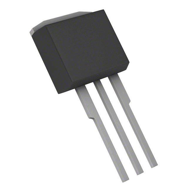
ICGOO电子元器件商城为您提供SIR804DP-T1-GE3由Vishay设计生产,在icgoo商城现货销售,并且可以通过原厂、代理商等渠道进行代购。 SIR804DP-T1-GE3价格参考。VishaySIR804DP-T1-GE3封装/规格:晶体管 - FET,MOSFET - 单, 表面贴装 N 沟道 100V 60A(Tc) 6.25W(Ta),104W(Tc) PowerPAK® SO-8。您可以下载SIR804DP-T1-GE3参考资料、Datasheet数据手册功能说明书,资料中有SIR804DP-T1-GE3 详细功能的应用电路图电压和使用方法及教程。
Vishay Siliconix 的 SIR804DP-T1-GE3 是一款 P 沟道增强型 MOSFET,常用于需要高效功率控制的场景。其主要应用场景包括:

1. 电源管理:适用于笔记本电脑、服务器和通信设备中的 DC-DC 转换器和负载开关,实现高效的电能分配与管理。

2. 电池供电设备:在便携式电子产品(如平板电脑、移动电源)中作为电源开关或逆向电流保护器件,因其低导通电阻可减少功耗,延长电池寿命。

3. 电机驱动与负载控制:用于小型电机、继电器或电磁阀的开关控制,具备快速响应特性,适合工业自动化和消费类电器应用。

4. 汽车电子:应用于车载电源系统、LED 照明控制及电池管理系统(BMS),满足对可靠性和效率要求较高的场景。

该器件采用小型封装(如PowerPAK® SC-70),适合空间受限的设计,同时具备良好的热性能和高耐用性,适用于中低功率开关应用。
| 参数 | 数值 |
| 产品目录 | |
| 描述 | MOSFET N-CH 100V 60A PPAK SO-8MOSFET 100V 7.2mOhm@10V 60A N-Ch MV T-FET |
| 产品分类 | FET - 单分离式半导体 |
| FET功能 | 标准 |
| FET类型 | MOSFET N 通道,金属氧化物 |
| Id-ContinuousDrainCurrent | 60 A |
| Id-连续漏极电流 | 60 A |
| 品牌 | Vishay SiliconixVishay / Siliconix |
| 产品手册 | |
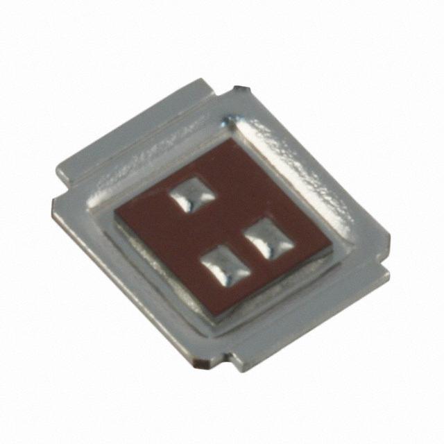
| 产品图片 |
|
| rohs | RoHS 合规性豁免无铅 / 符合限制有害物质指令(RoHS)规范要求 |
| 产品系列 | 晶体管,MOSFET,Vishay / Siliconix SIR804DP-T1-GE3TrenchFET® |
| 数据手册 | |
| 产品型号 | SIR804DP-T1-GE3SIR804DP-T1-GE3 |
| Pd-PowerDissipation | 104 W |
| Pd-功率耗散 | 104 W |
| Qg-GateCharge | 50.8 nC |
| Qg-栅极电荷 | 50.8 nC |
| RdsOn-Drain-SourceResistance | 7.2 mOhms |
| RdsOn-漏源导通电阻 | 7.2 mOhms |
| Vds-Drain-SourceBreakdownVoltage | 100 V |
| Vds-漏源极击穿电压 | 100 V |
| Vgs-Gate-SourceBreakdownVoltage | +/- 20 V |
| Vgs-栅源极击穿电压 | 20 V |
| 上升时间 | 9 nS |
| 下降时间 | 11 nS |
| 不同Id时的Vgs(th)(最大值) | 3V @ 250µA |
| 不同Vds时的输入电容(Ciss) | 2450pF @ 50V |
| 不同Vgs时的栅极电荷(Qg) | 76nC @ 10V |
| 不同 Id、Vgs时的 RdsOn(最大值) | 7.2 毫欧 @ 20A,10V |
| 产品种类 | MOSFET |
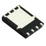
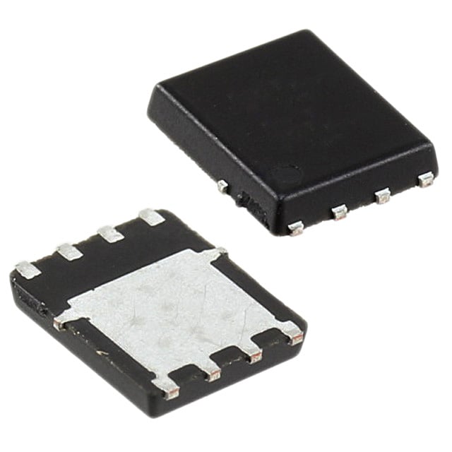
| 供应商器件封装 | PowerPAK® SO-8 |
| 其它名称 | SIR804DP-T1-GE3TR |
| 典型关闭延迟时间 | 38 nS |
| 功率-最大值 | 104W |
| 包装 | 带卷 (TR) |
| 商标 | Vishay / Siliconix |
| 安装类型 | 表面贴装 |
| 安装风格 | SMD/SMT |
| 封装 | Reel |
| 封装/外壳 | PowerPAK® SO-8 |
| 封装/箱体 | PowerPAK SO-8 |
| 工厂包装数量 | 3000 |
| 晶体管极性 | N-Channel |
| 最大工作温度 | + 150 C |
| 最小工作温度 | - 55 C |
| 标准包装 | 3,000 |
| 正向跨导-最小值 | 73 S |
| 漏源极电压(Vdss) | 100V |
| 特色产品 | http://www.digikey.com/product-highlights/cn/zh/vishay-thunderfet/1150 |
| 电流-连续漏极(Id)(25°C时) | 60A (Tc) |
| 系列 | SIRxxxDP |
| 配置 | Single |
| 零件号别名 | SIR804DP-GE3 |


- 商务部:美国ITC正式对集成电路等产品启动337调查
- 曝三星4nm工艺存在良率问题 高通将骁龙8 Gen1或转产台积电
- 太阳诱电将投资9.5亿元在常州建新厂生产MLCC 预计2023年完工
- 英特尔发布欧洲新工厂建设计划 深化IDM 2.0 战略
- 台积电先进制程称霸业界 有大客户加持明年业绩稳了
- 达到5530亿美元!SIA预计今年全球半导体销售额将创下新高
- 英特尔拟将自动驾驶子公司Mobileye上市 估值或超500亿美元
- 三星加码芯片和SET,合并消费电子和移动部门,撤换高东真等 CEO
- 三星电子宣布重大人事变动 还合并消费电子和移动部门
- 海关总署:前11个月进口集成电路产品价值2.52万亿元 增长14.8%


PDF Datasheet 数据手册内容提取
New Product SiR804DP Vishay Siliconix N-Channel 100 V (D-S) MOSFET FEATURES PRODUCT SUMMARY • Halogen-free According to IEC 61249-2-21 VDS (V) RDS(on) () ID (A)a Qg (Typ.) Definition 0.0072 at VGS = 10 V 60 (cid:129) TrenchFET® Power MOSFET 100 0.0078 at VGS = 7.5 V 60 24.8 nC (cid:129) 100 % Rg Tested 0.0103 at VGS = 4.5 V 60 (cid:129) 100 % UIS Tested (cid:129) Compliant to RoHS Directive 2002/95/EC PowerPAK® SO-8 APPLICATIONS (cid:129) Fixed Telecom 6.15 mm S 5.15 mm (cid:129) DC/DC Converter 1 S D 2 (cid:129) Primary Side Switch S 3 G 4 D 8 D 7 G D 6 D 5 Bottom View S Ordering Information: SiR804DP-T1-GE3 (Lead (Pb)-free and Halogen-free) N-Channel MOSFET ABSOLUTE MAXIMUM RATINGS (T = 25 °C, unless otherwise noted) A Parameter Symbol Limit Unit Drain-Source Voltage VDS 100 V Gate-Source Voltage VGS ± 20 TC = 25 °C 60a Continuous Drain Current (T = 150 °C) TC = 70 °C I 60a J TA = 25 °C D 20.8b, c TA = 70 °C 16.6b, c A Pulsed Drain Current IDM 100 Continuous Source-Drain Diode Current TTCA == 2255 °°CC IS 56.60ba, c Single Pulse Avalanche Current L =0.1 mH IAS 35 Single Pulse Avalanche Energy EAS 61 mJ TC = 25 °C 104 Maximum Power Dissipation TC = 70 °C PD 66.6 W TA = 25 °C 6.25b, c TA = 70 °C 4.0b, c Operating Junction and Storage Temperature Range TJ, Tstg - 55 to 150 °C Soldering Recommendations (Peak Temperature)d, e 260 THERMAL RESISTANCE RATINGS Parameter Symbol Typical Maximum Unit Maximum Junction-to-Ambientb, f t 10 s RthJA 15 20 °C/W Maximum Junction-to-Case (Drain) Steady State RthJC 0.9 1.2 Notes: a.Package limited. b.Surface mounted on 1" x 1" FR4 board. c. t = 10 s. d.See solder profile (www.vishay.com/ppg?73257). The PowerPAK SO-8 is a leadless package. The end of the lead terminal is exposed copper (not plated) as a result of the singulation process in manufacturing. A solder fillet at the exposed copper tip cannot be guaranteed and is not required to ensure adequate bottom side solder interconnection. e.Rework conditions: manual soldering with a soldering iron is not recommended for leadless components. f. Maximum under steady state conditions is 54 °C/W. Document Number: 65703 www.vishay.com S10-2680-Rev. B, 22-Nov-10 1
New Product SiR804DP Vishay Siliconix SPECIFICATIONS (T = 25 °C, unless otherwise noted) J Parameter Symbol Test Conditions Min. Typ. Max. Unit Static Drain-Source Breakdown Voltage VDS VGS = 0 V, ID = 250 µA 100 V VDS Temperature Coefficient VDS/TJ 51 ID = 250 µA mV/°C VGS(th) Temperature Coefficient VGS(th)/TJ - 6.0 Gate-Source Threshold Voltage VGS(th) VDS = VGS, ID = 250 µA 1.2 3.0 V Gate-Source Leakage IGSS VDS = 0 V, VGS = ± 20 V ± 100 nA VDS = 100 V, VGS = 0 V 1 Zero Gate Voltage Drain Current IDSS µA VDS = 100 V, VGS = 0 V, TJ = 55 °C 10 On-State Drain Currenta ID(on) VDS 5 V, VGS = 10 V 30 A VGS = 10 V, ID = 20 A 0.0059 0.0072 Drain-Source On-State Resistancea RDS(on) VGS = 7.5 V, ID = 20 A 0.0063 0.0078 VGS = 4.5 V, ID = 15 A 0.0083 0.0103 Forward Transconductancea gfs VDS = 10 V, ID = 20 A 73 S Dynamicb Input Capacitance Ciss 2450 Output Capacitance Coss VDS = 50 V, VGS = 0 V, f = 1 MHz 1430 pF Reverse Transfer Capacitance Crss 80 VDS = 50 V, VGS = 10 V, ID = 20 A 50.8 76 Total Gate Charge Qg VDS = 50 V, VGS = 7.5 V, ID = 20 A 39.2 59 24.8 37.2 nC Gate-Source Charge Qgs VDS = 50 V, VGS = 4.5 V, ID = 20 A 8.1 Gate-Drain Charge Qgd 10.6 Gate Resistance Rg f = 1 MHz 0.4 2.0 4.0 Turn-On Delay Time td(on) 11 22 Rise Time tr VDD = 50 V, RL = 2.5 9 18 Turn-Off Delay Time td(off) ID 20 A, VGEN = 10 V, Rg = 1 38 70 Fall Time tf 11 22 ns Turn-On Delay Time td(on) 15 30 Rise Time tr VDD = 50 V, RL = 2.5 14 28 Turn-Off Delay Time td(off) ID 20 A, VGEN = 7.5 V, Rg = 1 35 70 Fall Time tf 10 20 Drain-Source Body Diode Characteristics Continuous Source-Drain Diode Current IS TC = 25 °C 60 A Pulse Diode Forward Currenta ISM 100 Body Diode Voltage VSD IS = 5 A 0.76 1.1 V Body Diode Reverse Recovery Time trr 56 100 ns Body Diode Reverse Recovery Charge Qrr 65 120 nC I = 20 A, dI/dt = 100 A/µs, T = 25 °C F J Reverse Recovery Fall Time ta 22 ns Reverse Recovery Rise Time tb 34 Notes: a. Pulse test; pulse width 300 µs, duty cycle 2 %. b. Guaranteed by design, not subject to production testing. Stresses beyond those listed under “Absolute Maximum Ratings” may cause permanent damage to the device. These are stress ratings only, and functional operation of the device at these or any other conditions beyond those indicated in the operational sections of the specifications is not implied. Exposure to absolute maximum rating conditions for extended periods may affect device reliability. www.vishay.com Document Number: 65703 2 S10-2680-Rev. B, 22-Nov-10
New Product SiR804DP Vishay Siliconix TYPICAL CHARACTERISTICS (25°C, unless otherwise noted) 100 10 VGS= 10 V thru 5 V 80 8 A) VGS= 4 V A) TC= 125 °C nt ( 60 nt ( 6 e e urr urr C C n n ai 40 ai 4 Dr Dr - D - D TC= 25 °C I I 20 2 VGS= 3 V TC= - 55 °C 0 0 0.0 0.5 1.0 1.5 2.0 2.5 0 1 2 3 4 5 VDS- Drain-to-Source Voltage (V) VGS- Gate-to-Source Voltage (V) Output Characteristics Transfer Characteristics 0.0125 4500 Ciss 0.0110 3600 Ω) ance ( 0.0095 VGS= 4.5 V e (pF) 2700 sist anc Re cit n- pa Coss O 0.0080 a 1800 - S(on) VGS= 7.5 V C - C D R 0.0065 900 VGS= 10 V Crss 0.0050 0 0 20 40 60 80 100 0 20 40 60 80 100 ID- Drain Current (A) VDS- Drain-to-Source Voltage (V) On-Resistance vs. Drain Current and Gate Voltage Capacitance 10 2.1 ID= 20 A ID=20A age (V) 8 VDS= 25 V ce 1.8 VGS= 10 V e-to-Source Volt 46 VDS= 50 V VDS= 75 V - On-Resistann)(Normalized) 11..25 VGS= 4.5 V Gat S(o - GS 2 RD 0.9 V 0 0.6 0.0 10.6 21.2 31.8 42.4 53.0 - 50 - 25 0 25 50 75 100 125 150 Qg- Total Gate Charge (nC) TJ- Junction Temperature (°C) Gate Charge On-Resistance vs. Junction Temperature Document Number: 65703 www.vishay.com S10-2680-Rev. B, 22-Nov-10 3
New Product SiR804DP Vishay Siliconix TYPICAL CHARACTERISTICS (25°C, unless otherwise noted) 0.05 100 ID = 20 A TJ= 150 °C 0.04 10 W) ent (A) 1 TJ= 25 °C ance ( 0.03 Curr esist e R urc 0.1 On- 0.02 - SoIS - DS(on) 0.01 TJ= 125 °C 0.01 R TJ= 25 °C 0.00 0.001 0.0 0.2 0.4 0.6 0.8 1.0 1.2 0 2 4 6 8 10 VSD- Source-to-Drain Voltage (V) VGS- Gate-to-Source Voltage (V) Source-Drain Diode Forward Voltage On-Resistance vs. Gate-to-Source Voltage 0.5 200 0.2 160 V) ce ( - 0.1 W) 120 n VariaS(th) - 0.4 ID= 5 mA Power ( 80 G V - 0.7 40 ID= 250 µA - 1.0 0 - 50 - 25 0 25 50 75 100 125 150 0.001 0.01 0.1 1 10 TJ- Temperature (°C) Time (s) Single Pulse Power, Junction-to-Ambient Threshold Voltage 100 Limited by RDS(on)* 10 1 ms A) nt ( e 10 ms Curr 1 ain 100 ms Dr - D 1 s I 0.1 10 s TA= 25 °C BVDSS Limited DC Single Pulse 0.01 0.01 0.1 1 10 100 VDS- Drain-to-SourceVoltage(V) * VGS>minimum VGSat which RDS(on)is specified Safe Operating Area, Junction-to-Ambient www.vishay.com Document Number: 65703 4 S10-2680-Rev. B, 22-Nov-10
New Product SiR804DP Vishay Siliconix TYPICAL CHARACTERISTICS (25°C, unless otherwise noted) 100 80 nt (A) 60 Package Limited e urr C n Drai 40 - D I 20 0 0 25 50 75 100 125 150 TC- Case Temperature (°C) Current Derating* 125 3.0 100 2.4 W) 75 W) 1.8 wer ( wer ( Po 50 Po 1.2 25 0.6 0 0.0 0 25 50 75 100 125 150 0 25 50 75 100 125 150 TC - Case Temperature (°C) TA- Ambient Temperature (°C) Power, Junction-to-Case Power, Junction-to-Ambient * The power dissipation P is based on T = 150 °C, using junction-to-case thermal resistance, and is more useful in settling the upper D J(max) dissipation limit for cases where additional heatsinking is used. It is used to determine the current rating, when this rating falls below the package limit. Document Number: 65703 www.vishay.com S10-2680-Rev. B, 22-Nov-10 5
New Product SiR804DP Vishay Siliconix TYPICAL CHARACTERISTICS (25°C, unless otherwise noted) 1 Duty Cycle = 0.5 nt e Transiance 0.2 ctive mped 0.1 Notes: ed Effeermal I 0.1 0.05 PDM zh maliT t1 Nor 0.02 1.DutyCyclet,2D= t1 t2 2.PerUnitBase=RthJA=54 °C/W 3.TJM--TA=PDMZthJA(t) Single Pulse 4.SurfaceMounted 0.01 10-4 10-3 10-2 10-1 1 10 100 1000 Square Wave Pulse Duration (s) Normalized Thermal Transient Impedance, Junction-to-Ambient 1 Duty Cycle = 0.5 nt Transieance 00..12 ctive mped 0.05 zed Effehermal I 0.1 Single Pulse 0.02 aliT m or N 0.01 10-4 10-3 10-2 10-1 1 10 Square Wave Pulse Duration (s) Normalized Thermal Transient Impedance, Junction-to-Case Vishay Siliconix maintains worldwide manufacturing capability. Products may be manufactured at one of several qualified locations. Reliability data for Silicon Technology and Package Reliability represent a composite of all qualified locations. For related documents such as package/tape drawings, part marking, and reliability data, see www.vishay.com/ppg?65703. www.vishay.com Document Number: 65703 6 S10-2680-Rev. B, 22-Nov-10
Package Information www.vishay.com Vishay Siliconix PowerPAK® SO-8, (Single/Dual) H L E2 K W E4 θ D4 1 M 1 Z 2 2 e 2D1D D2 D D5 3 3 4 4b θ L1 E3 θ θ A1 Backside View of Single Pad H E2 K L A E4 c 2 4 E1 Detail Z D 1 E D3 (2x) D1 2 D2 K1 D5 3 D2 4b Notes 1.Inch will govern. 2 Dimensions exclusive of mold gate burrs. E3 3.Dimensions exclusive of mold flash and cutting burrs. Backside View of Dual Pad MILLIMETERS INCHES DIM. MIN. NOM. MAX. MIN. NOM. MAX. A 0.97 1.04 1.12 0.038 0.041 0.044 A1 - 0.05 0 - 0.002 b 0.33 0.41 0.51 0.013 0.016 0.020 c 0.23 0.28 0.33 0.009 0.011 0.013 D 5.05 5.15 5.26 0.199 0.203 0.207 D1 4.80 4.90 5.00 0.189 0.193 0.197 D2 3.56 3.76 3.91 0.140 0.148 0.154 D3 1.32 1.50 1.68 0.052 0.059 0.066 D4 0.57 typ. 0.0225 typ. D5 3.98 typ. 0.157 typ. E 6.05 6.15 6.25 0.238 0.242 0.246 E1 5.79 5.89 5.99 0.228 0.232 0.236 E2 3.48 3.66 3.84 0.137 0.144 0.151 E3 3.68 3.78 3.91 0.145 0.149 0.154 E4 0.75 typ. 0.030 typ. e 1.27 BSC 0.050 BSC K 1.27 typ. 0.050 typ. K1 0.56 - - 0.022 - - H 0.51 0.61 0.71 0.020 0.024 0.028 L 0.51 0.61 0.71 0.020 0.024 0.028 L1 0.06 0.13 0.20 0.002 0.005 0.008 0° - 12° 0° - 12° W 0.15 0.25 0.36 0.006 0.010 0.014 M 0.125 typ. 0.005 typ. ECN: S17-0173-Rev. L, 13-Feb-17 DWG: 5881 Revison: 13-Feb-17 1 Document Number: 71655 THIS DOCUMENT IS SUBJECT TO CHANGE WITHOUT NOTICE. THE PRODUCTS DESCRIBED HEREIN AND THIS DOCUMENT ARE SUBJECT TO SPECIFIC DISCLAIMERS, SET FORTH AT www.vishay.com/doc?91000
VISHAY SILICONIX www.vishay.com Power MOSFETs Application Note AN821 PowerPAK® SO-8 Mounting and Thermal Considerations by Wharton McDaniel PowerPAK SO-8 SINGLE MOUNTING MOSFETs for switching applications are now available with The PowerPAK single is simple to use. The pin arrangement die on resistances around 1 m and with the capability to (drain, source, gate pins) and the pin dimensions are the handle 85 A. While these die capabilities represent a major same as standard SO-8 devices (see figure 2). Therefore, the advance over what was available just a few years ago, it is PowerPAK connection pads match directly to those of the important for power MOSFET packaging technology to keep SO-8. The only difference is the extended drain connection pace. It should be obvious that degradation of a high area. To take immediate advantage of the PowerPAK SO-8 performance die by the package is undesirable. PowerPAK single devices, they can be mounted to existing SO-8 land is a new package technology that addresses these issues. patterns. In this application note, PowerPAK’s construction is described. Following this mounting information is presented including land patterns and soldering profiles for maximum reliability. Finally, thermal and electrical performance is discussed. THE PowerPAK PACKAGE The PowerPAK package was developed around the SO-8 package (figure 1). The PowerPAK SO-8 utilizes the same footprint and the same pin-outs as the standard SO-8. This Standard SO-8 PowerPAK SO-8 allows PowerPAK to be substituted directly for a standard SO-8 package. Being a leadless package, PowerPAK SO-8 Fig. 2 utilizes the entire SO-8 footprint, freeing space normally occupied by the leads, and thus allowing it to hold a larger The minimum land pattern recommended to take full die than a standard SO-8. In fact, this larger die is slightly advantage of the PowerPAK thermal performance see larger than a full sized DPAK die. The bottom of the die Application Note 826, Recommended Minimum Pad attach pad is exposed for the purpose of providing a direct, Patterns With Outline Drawing Access for Vishay Siliconix low resistance thermal path to the substrate the device is MOSFETs. Click on the PowerPAK SO-8 single in the index mounted on. Finally, the package height is lower than the of this document. standard SO-8, making it an excellent choice for applications with space constraints. In this figure, the drain land pattern is given to make full contact to the drain pad on the PowerPAK package. This land pattern can be extended to the left, right, and top of the drawn pattern. This extension will serve to increase the heat dissipation by decreasing the thermal resistance A from the foot of the PowerPAK to the PC board and P therefore to the ambient. Note that increasing the drain land P area beyond a certain point will yield little decrease L in foot-to-board and foot-to-ambient thermal resistance. I Under specific conditions of board configuration, copperC weight and layer stack, experiments have found thatA more than about 0.25 in2 to 0.5 in2 of additional copperT (in addition to the drain land) will yield little improvement inI O thermal performance. N N Fig. 1 PowerPAK 1212 Devices O T Revision: 16-Mai-13 1 Document Number: 71622 E For technical questions, contact: powermosfettechsupport@vishay.com THIS DOCUMENT IS SUBJECT TO CHANGE WITHOUT NOTICE. THE PRODUCTS DESCRIBED HEREIN AND THIS DOCUMENT ARE SUBJECT TO SPECIFIC DISCLAIMERS, SET FORTH AT www.vishay.com/doc?91000
Application Note AN821 www.vishay.com Vishay Siliconix PowerPAK® SO-8 Mounting and Thermal Considerations PowerPAK SO-8 DUAL For the lead (Pb)-free solder profile, see www.vishay.com/doc?73257. The pin arrangement (drain, source, gate pins) and the pin dimensions of the PowerPAK SO-8 dual are the same as standard SO-8 dual devices. Therefore, the PowerPAK device connection pads match directly to those of the SO-8. As in the single-channel package, the only exception is the extended drain connection area. Manufacturers can likewise take immediate advantage of the PowerPAK SO-8 dual devices by mounting them to existing SO-8 dual land patterns. To take the advantage of the dual PowerPAK SO-8’s thermal performance, the minimum recommended land pattern can be found in Application Note 826, Recommended Minimum Pad Patterns With Outline Drawing Access for Vishay Siliconix MOSFETs. Click on the PowerPAK 1212-8 dual in the index of this document. The gap between the two drain pads is 24 mils. This matches the spacing of the two drain pads on the Fig. 3 Solder Reflow Temperature Profile PowerPAK SO-8 dual package. REFLOW SOLDERING Ramp-Up Rate + 3 °C /s max. Temperature at 150 - 200 °C 120 s max. Vishay Siliconix surface-mount packages meet solder reflow reliability requirements. Devices are subjected to solder Temperature Above 217 °C 60 - 150 s reflow as a test preconditioning and are then Maximum Temperature 255 + 5/- 0 °C reliability-tested using temperature cycle, bias humidity, Time at Maximum 30 s HAST, or pressure pot. The solder reflow temperature profile Temperature used, and the temperatures and time duration, are shown in Ramp-Down Rate + 6 °C/s max. figures 3 and 4. 30 s 260 °C 3 °C(max) 6 °C /s (max.) 217 °C 150 - 200 °C 150 s (max.) 60 s (min.) Reflow Zone E Pre-Heating Zone T O N Maximum peak temperature at 240 °C is allowed. N O I T Fig. 4 Solder Reflow Temperatures and Time Durations A C I L P PRevision: 16-Mai-13 2 Do cument Number: 71622 A For technical questions, contact: powermosfettechsupport@vishay.com THIS DOCUMENT IS SUBJECT TO CHANGE WITHOUT NOTICE. THE PRODUCTS DESCRIBED HEREIN AND THIS DOCUMENT ARE SUBJECT TO SPECIFIC DISCLAIMERS, SET FORTH AT www.vishay.com/doc?91000
Application Note AN821 www.vishay.com Vishay Siliconix PowerPAK® SO-8 Mounting and Thermal Considerations THERMAL PERFORMANCE Introduction Because of the presence of the trough, this result suggests A basic measure of a device’s thermal performance a minimum performance improvement of 10 °C/W by using is the junction-to-case thermal resistance, R , or the a PowerPAK SO-8 in a standard SO-8 PC board mount. thJC junction-to-foot thermal resistance, R This parameter is The only concern when mounting a PowerPAK on a thJF measured for the device mounted to an infinite heat sink and standard SO-8 pad pattern is that there should be no traces is therefore a characterization of the device only, in other running between the body of the MOSFET. Where the words, independent of the properties of the object to which standard SO-8 body is spaced away from the pc board, the device is mounted. Table 1 shows a comparison of allowing traces to run underneath, the PowerPAK sits the DPAK, PowerPAK SO-8, and standard SO-8. The directly on the pc board. PowerPAK has thermal performance equivalent to the Thermal Performance - Spreading Copper DPAK, while having an order of magnitude better thermal Designers may add additional copper, spreading copper, to performance over the SO-8. the drain pad to aid in conducting heat from a device. It is TABLE 1 - DPAK AND POWERPAK SO-8 helpful to have some information about the thermal EQUIVALENT STEADY STATE performance for a given area of spreading copper. PERFORMANCE Figure 6 shows the thermal resistance of a PowerPAK SO-8 device mounted on a 2-in. 2-in., four-layer FR-4 PC board. PowerPAK Standard DPAK The two internal layers and the backside layer are solid SO-8 SO-8 copper. The internal layers were chosen as solid copper to Thermal 1.2 °C/W 1 °C/W 16 °C/W model the large power and ground planes common in many Resistance R thJC applications. The top layer was cut back to a smaller area and at each step junction-to-ambient thermal resistance Thermal Performance on Standard SO-8 Pad Pattern measurements were taken. The results indicate that an area Because of the common footprint, a PowerPAK SO-8 above 0.3 to 0.4 square inches of spreading copper gives no can be mounted on an existing standard SO-8 pad pattern. additional thermal performance improvement. A The question then arises as to the thermal performance subsequent experiment was run where the copper on the of the PowerPAK device under these conditions. A back-side was reduced, first to 50 % in stripes to mimic characterization was made comparing a standard SO-8 and circuit traces, and then totally removed. No significant effect a PowerPAK device on a board with a trough cut out was observed. underneath the PowerPAK drain pad. This configuration restricted the heat flow to the SO-8 land pads. The results are shown in figure 5. (0 %R, t5h 0v s%. ,S 1p0re0a %di nBga Ccko pCpoeprper) 56 Si4874DY vs. Si7446DP PPAK on a 4-Layer Board SO-8 Pattern, Trough Under Drain 60 )s 51 tta 50 w/C )s ( e ttaw 40 cna 46 E /( eC Si4874DY depm T cn 30 I O adep Si7446DP 41 100 % m 0 % N I 20 50 % N 10 36 O 0.00 0.25 0.50 0.75 1.00 1.25 1.50 1.75 2.00 I Spreading Copper (sq in) T 0 A 0.0001 0.01 1 100 10000 Fig. 6 Spreading Copper Junction-to-Ambient Performance C Pulse Duration (sec) I Fig. 5 PowerPAK SO-8 and Standard SO-0 Land Pad Thermal L Path P PRevision: 16-Mai-13 3 Do cument Number: 71622 A For technical questions, contact: powermosfettechsupport@vishay.com THIS DOCUMENT IS SUBJECT TO CHANGE WITHOUT NOTICE. THE PRODUCTS DESCRIBED HEREIN AND THIS DOCUMENT ARE SUBJECT TO SPECIFIC DISCLAIMERS, SET FORTH AT www.vishay.com/doc?91000
Application Note AN821 www.vishay.com Vishay Siliconix PowerPAK® SO-8 Mounting and Thermal Considerations SYSTEM AND ELECTRICAL IMPACT OF Suppose each device is dissipating 2.7 W. Using the PowerPAK SO-8 junction-to-foot thermal resistance characteristics of the PowerPAK SO-8 and the standard SO-8, the die In any design, one must take into account the change in temperature is determined to be 107 °C for the PowerPAK MOSFET R with temperature (figure 7). DS(on) (and for DPAK) and 148 °C for the standard SO-8. This is a 2 °C rise above the board temperature for the PowerPAK On-Resistance vs. Junction Temperature and a 43 °C rise for the standard SO-8. Referring to figure 7, 1.8 a 2 °C difference has minimal effect on R whereas a DS(on) )dezilam 1.6 VID G =S 2=3 1 0 A V M43in °iCm idziifnfegr tehnec teh hearms aal sriisgen iafibcoavnet ethffee cbto oanrd R tDeSm(opn)e. rature by roN using PowerPAK has not only eased the thermal design but ( ) 1.4 it has allowed the device to run cooler, keep rDS(on) low, and ( e permits the device to handle more current than the same c na 1.2 MOSFET die in the standard SO-8 package. ts is e R CONCLUSIONS -n 1.0 O - PowerPAK SO-8 has been shown to have the same thermal )n 0.8 performance as the DPAK package while having the same o (S footprint as the standard SO-8 package. The PowerPAK D R SO-8 can hold larger die approximately equal in size to the 0.6 -50 -25 0 25 50 75 100 125 150 maximum that the DPAK can accommodate implying no sacrifice in performance because of package limitations. TJ - Junction Temperature (°C) Recommended PowerPAK SO-8 land patterns are provided Fig. 7 MOSFET R vs. Temperature to aid in PC board layout for designs using this new DS(on) A MOSFET generates internal heat due to the current package. passing through the channel. This self-heating raises the Thermal considerations have indicated that significant junction temperature of the device above that of the PC advantages can be gained by using PowerPAK SO-8 board to which it is mounted, causing increased power devices in designs where the PC board was laid out for dissipation in the device. A major source of this problem lies the standard SO-8. Applications experimental data gave in the large values of the junction-to-foot thermal resistance thermal performance data showing minimum and of the SO-8 package. typical thermal performance in a SO-8 environment, plus PowerPAK SO-8 minimizes the junction-to-board thermal information on the optimum thermal performance resistance to where the MOSFET die temperature is very obtainable including spreading copper. This further close to the temperature of the PC board. Consider two emphasized the DPAK equivalency. devices mounted on a PC board heated to 105 °C by other PowerPAK SO-8 therefore has the desired small size components on the board (figure 8). characteristics of the SO-8 combined with the attractive thermal characteristics of the DPAK package. PowerPAK SO-8 Standard SO-8 107 °C 148 °C E T O N 0.8 °C/W 16 C/W N PC Board at 105 °C O I T A C I L Fig. 8 Temperature of Devices on a PC Board P PRevision: 16-Mai-13 4 Do cument Number: 71622 A For technical questions, contact: powermosfettechsupport@vishay.com THIS DOCUMENT IS SUBJECT TO CHANGE WITHOUT NOTICE. THE PRODUCTS DESCRIBED HEREIN AND THIS DOCUMENT ARE SUBJECT TO SPECIFIC DISCLAIMERS, SET FORTH AT www.vishay.com/doc?91000
Application Note 826 Vishay Siliconix RECOMMENDED MINIMUM PADS FOR PowerPAK® SO-8 Single 0.260 (6.61) 0.150 (3.81) 0.024 (0.61) (00..06266) 0.154 (3.91) 0.174 (4.42) 0.050 (1.27) 0.050 0.032 0.040 (1.27) (0.82) (1.02) Recommended Minimum Pads Dimensions in Inches/(mm) Return to Index Return to Index A P P L I C A T I O N N O T E Document Number: 72599 www.vishay.com Revision: 21-Jan-08 15
Legal Disclaimer Notice www.vishay.com Vishay Disclaimer ALL PRODUCT, PRODUCT SPECIFICATIONS AND DATA ARE SUBJECT TO CHANGE WITHOUT NOTICE TO IMPROVE RELIABILITY, FUNCTION OR DESIGN OR OTHERWISE. Vishay Intertechnology, Inc., its affiliates, agents, and employees, and all persons acting on its or their behalf (collectively, “Vishay”), disclaim any and all liability for any errors, inaccuracies or incompleteness contained in any datasheet or in any other disclosure relating to any product. Vishay makes no warranty, representation or guarantee regarding the suitability of the products for any particular purpose or the continuing production of any product. To the maximum extent permitted by applicable law, Vishay disclaims (i) any and all liability arising out of the application or use of any product, (ii) any and all liability, including without limitation special, consequential or incidental damages, and (iii) any and all implied warranties, including warranties of fitness for particular purpose, non-infringement and merchantability. Statements regarding the suitability of products for certain types of applications are based on Vishay’s knowledge of typical requirements that are often placed on Vishay products in generic applications. Such statements are not binding statements about the suitability of products for a particular application. It is the customer’s responsibility to validate that a particular product with the properties described in the product specification is suitable for use in a particular application. Parameters provided in datasheets and / or specifications may vary in different applications and performance may vary over time. All operating parameters, including typical parameters, must be validated for each customer application by the customer’s technical experts. Product specifications do not expand or otherwise modify Vishay’s terms and conditions of purchase, including but not limited to the warranty expressed therein. Except as expressly indicated in writing, Vishay products are not designed for use in medical, life-saving, or life-sustaining applications or for any other application in which the failure of the Vishay product could result in personal injury or death. Customers using or selling Vishay products not expressly indicated for use in such applications do so at their own risk. Please contact authorized Vishay personnel to obtain written terms and conditions regarding products designed for such applications. No license, express or implied, by estoppel or otherwise, to any intellectual property rights is granted by this document or by any conduct of Vishay. Product names and markings noted herein may be trademarks of their respective owners. © 2017 VISHAY INTERTECHNOLOGY, INC. ALL RIGHTS RESERVED Revision: 08-Feb-17 1 Document Number: 91000
Mouser Electronics Authorized Distributor Click to View Pricing, Inventory, Delivery & Lifecycle Information: V ishay: SIR804DP-T1-GE3