ICGOO在线商城 > 分立半导体产品 > 晶体管 - FET,MOSFET - 单 > SN7002N L6327
 Datasheet下载
- 型号: SN7002N L6327
- 制造商: Infineon
- 库位|库存: xxxx|xxxx
- 要求:
| 数量阶梯 | 香港交货 | 国内含税 |
| +xxxx | $xxxx | ¥xxxx |
查看当月历史价格
查看今年历史价格
SN7002N L6327产品简介:
ICGOO电子元器件商城为您提供SN7002N L6327由Infineon设计生产,在icgoo商城现货销售,并且可以通过原厂、代理商等渠道进行代购。 SN7002N L6327价格参考。InfineonSN7002N L6327封装/规格:晶体管 - FET,MOSFET - 单, N-Channel 60V 200mA (Ta) 360mW (Ta) Surface Mount SOT-23-3。您可以下载SN7002N L6327参考资料、Datasheet数据手册功能说明书,资料中有SN7002N L6327 详细功能的应用电路图电压和使用方法及教程。
Infineon Technologies 的型号为 SN7002N L6327 的产品实际上存在信息混淆。SN7002N 是 Texas Instruments(德州仪器)生产的 N 沟道 MOSFET,而非 Infineon Technologies(英飞凌)的产品;L6327 则是 Infineon 常用的卷带编码,并非具体型号。因此,该组合可能为误标或混淆型号。

若讨论的是 Infineon 的类似规格 N 沟道 MOSFET(如其 OptiMOS™ 或 StrongIRFET™ 系列中用于小功率开关的器件),这类晶体管通常应用于以下场景:

1. 电源管理:在DC-DC转换器、电压调节模块(VRM)中作为开关元件,提高能效。
2. 负载开关:用于控制便携设备(如手机、平板)中的电源通断,防止浪涌电流。
3. 电机驱动:在小型直流电机或步进电机控制电路中实现低功耗驱动。
4. LED驱动:作为开关控制LED照明的亮灭与调光。
5. 工业与消费类电子:广泛用于电源适配器、智能电表、家电控制板等。

此类MOSFET具有低导通电阻(RDS(on))、快速开关速度和高可靠性,适合高频、高效率的小功率应用。建议核对实际型号以确保选型准确。
| 参数 | 数值 |
| 产品目录 | |
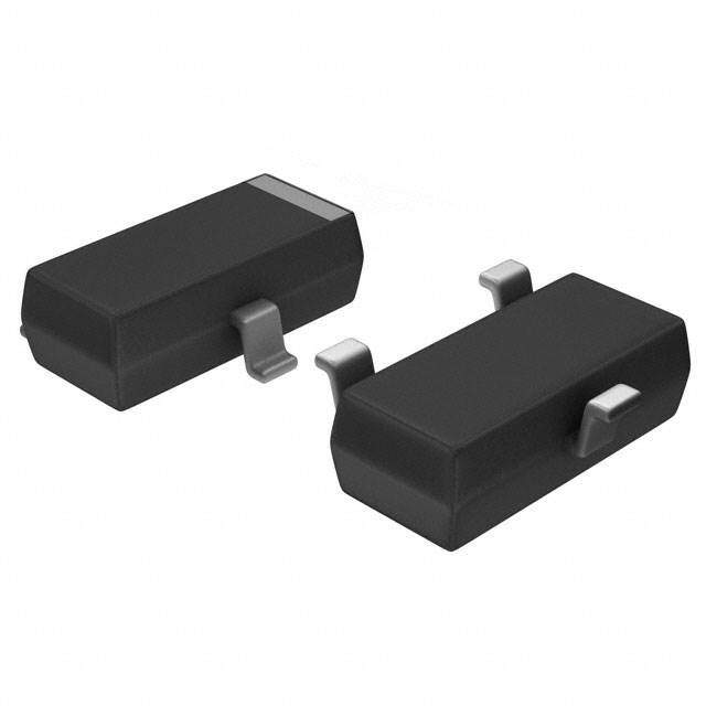
| 描述 | MOSFET N-CH 60V 200MA SOT-23 |
| 产品分类 | FET - 单 |
| FET功能 | 逻辑电平门 |
| FET类型 | MOSFET N 通道,金属氧化物 |
| 品牌 | Infineon Technologies |
| 数据手册 | |
| 产品图片 |
|
| 产品型号 | SN7002N L6327 |
| PCN过时产品 | |
| rohs | 无铅 / 符合限制有害物质指令(RoHS)规范要求 |
| 产品系列 | SIPMOS® |
| 不同Id时的Vgs(th)(最大值) | 1.8V @ 26µA |
| 不同Vds时的输入电容(Ciss) | 45pF @ 25V |
| 不同Vgs时的栅极电荷(Qg) | 1.5nC @ 10V |
| 不同 Id、Vgs时的 RdsOn(最大值) | 5 欧姆 @ 500mA,10V |
| 产品目录页面 | |
| 供应商器件封装 | PG-SOT23-3 |
| 其它名称 | SN7002NL6327 |
| 功率-最大值 | 360mW |
| 包装 | 剪切带 (CT) |
| 安装类型 | 表面贴装 |
| 封装/外壳 | TO-236-3,SC-59,SOT-23-3 |
| 标准包装 | 1 |
| 漏源极电压(Vdss) | 60V |
| 电流-连续漏极(Id)(25°C时) | 200mA (Ta) |


- 商务部:美国ITC正式对集成电路等产品启动337调查
- 曝三星4nm工艺存在良率问题 高通将骁龙8 Gen1或转产台积电
- 太阳诱电将投资9.5亿元在常州建新厂生产MLCC 预计2023年完工
- 英特尔发布欧洲新工厂建设计划 深化IDM 2.0 战略
- 台积电先进制程称霸业界 有大客户加持明年业绩稳了
- 达到5530亿美元!SIA预计今年全球半导体销售额将创下新高
- 英特尔拟将自动驾驶子公司Mobileye上市 估值或超500亿美元
- 三星加码芯片和SET,合并消费电子和移动部门,撤换高东真等 CEO
- 三星电子宣布重大人事变动 还合并消费电子和移动部门
- 海关总署:前11个月进口集成电路产品价值2.52万亿元 增长14.8%


PDF Datasheet 数据手册内容提取
SN7002N (cid:210) SIPMOS Small-Signal-Transistor Product Summary Feature V 60 V • N-Channel DS R 5 W • Enhancement mode DS(on) I 0.2 A • Logic Level D • dv/dt rated PG-SOT-23 Drain pin 3 • Qualified according to AEC Q101 Gate pin1 Source pin 2 Type Package Pb-free Tape and Reel Information Marking SN7002N PG-SOT-23 Yes L6327: 3000 pcs/reel sSN SN7002N PG-SOT-23 Yes L6433: 10000 pcs/reel sSN Maximum Ratings, at T = 25 °C, unless otherwise specified j Parameter Symbol Value Unit Continuous drain current I A D TA=25°C 0.2 TA=70°C 0.16 Pulsed drain current I 0.8 D puls TA=25°C Reverse diode dv/dt dv/dt 6 kV/µs IS=0.2A, VDS=48V, di/dt=200A/µs, Tjmax=150°C Gate source voltage V ±20 V GS ESD Class (JESD22-A114-HBM) 0 (<250V) Power dissipation P 0.36 W tot TA=25°C Operating and storage temperature Tj , Tstg -55... +150 °C IEC climatic category; DIN IEC 68-1 55/150/56 Rev. 2.5 Page 1 2009-14-08
SN7002N Thermal Characteristics Parameter Symbol Values Unit min. typ. max. Characteristics Thermal resistance, junction - ambient R - - 350 K/W thJA at minimal footprint Electrical Characteristics, at T = 25 °C, unless otherwise specified j Parameter Symbol Values Unit min. typ. max. Static Characteristics Drain-source breakdown voltage V 60 - - V (BR)DSS V =0, I =250µA GS D Gate threshold voltage, V = V V 0.8 1.4 1.8 GS DS GS(th) I =26µA D Zero gate voltage drain current I µA DSS V =60V, V =0, T=25°C - - 0.1 DS GS j V =60V, V =0, T=150°C - - 5 DS GS j Gate-source leakage current I - - 10 nA GSS V =20V, V =0 GS DS Drain-source on-state resistance R - 3.9 7.5 W DS(on) V =4.5V, I =0.17A GS D Drain-source on-state resistance R - 2.5 5 DS(on) V =10V, I =0.5A GS D Rev. 2.5 Page 2 2009-14-08
SN7002N Electrical Characteristics, at T = 25 °C, unless otherwise specified j Parameter Symbol Conditions Values Unit min. typ. max. Dynamic Characteristics Transconductance g V ‡ 2*I *R , 0.09 0.17 - S fs DS D DS(on)max I =0.16A D Input capacitance C V =0, V =25V, - 34 45 pF iss GS DS Output capacitance C f=1MHz - 7.2 9.6 oss Reverse transfer capacitance C - 2.8 4.2 rss Turn-on delay time t V =30V, V =10V, - 2.4 3.6 ns d(on) DD GS Rise time t I =0.5A, R =6W - 3.2 4.8 r D G Turn-off delay time t - 5.3 8 d(off) Fall time t - 3.6 5.4 f Gate Charge Characteristics Gate to source charge Q V =48V, I =0.5A - 0.14 0.21 nC gs DD D Gate to drain charge Q - 0.42 0.63 gd Gate charge total Q V =48V, I =0.5A, - 1 1.5 g DD D V =0 to 10V GS Gate plateau voltage V V =48V, I = 0.5 A - 4.5 - V (plateau) DD D Reverse Diode Inverse diode continuous I T =25°C - - 0.2 A S A forward current Inv. diode direct current, pulsedI - - 0.8 SM Inverse diode forward voltage V V =0, I = I - 0.83 1.2 V SD GS F S Reverse recovery time t V =30V, I =l , - 14.2 21.3 ns rr R F S Reverse recovery charge Q di /dt=100A/µs - 5.9 8.8 nC rr F Rev. 2.5 Page 3 2009-14-08
SN7002N 1 Power dissipation 2 Drain current P = f (T ) I = f (T ) tot A D A parameter: V ‡ 10 V GS SN7002N SN7002N 0.38 0.22 W A 0.32 0.18 0.28 0.16 Ptot 0.24 D 0.14 I 0.12 0.2 0.1 0.16 0.08 0.12 0.06 0.08 0.04 0.04 0.02 0 0 0 20 40 60 80 100 120 °C 160 0 20 40 60 80 100 120 °C 160 T T A A 3 Safe operating area 4 Transient thermal impedance I = f ( V ) Z = f (t ) D DS thJA p parameter : D = 0 , T = 25 °C parameter : D = t /T A p 10 1 SN7002N 10 3 SN7002N K/W A 10 2 10 0 tp = 2 0 0 .0 µ s ID R D S ( o n) = V D S / I D 1 ms ZthJA 10 1 10 -1 10 ms 10 0 D = 0.50 0.20 10 -1 0.10 0.05 10 -2 0.02 DC 10 -2 0.01 single pulse 10 -3 10 -3 10 0 10 1 V 10 2 10 -7 10 -6 10 -5 10 -4 10 -3 10 -2 s 10 0 V t DS p Rev. 2.5 Page 4 2009-14-08
SN7002N 5 Typ. output characteristic 6 Typ. drain-source on resistance I = f (V ) R = f (I ) D DS DS(on) D parameter: Tj = 25 °C, VGS parameter: Tj = 25 °C, VGS 1 7.5 3.1V 10V W 3.5V A 7V 3.7V 6V 4.1V 5V 6 4.5V 0.75 4.5V n) 5V 4.0V (o 5.25 6V 3.7V DS 7V D0.625 3.5V R 10V I 4.5 3.0V 0.5 3.75 3 0.375 2.25 0.25 1.5 0.125 0.75 0 0 0 0.5 1 1.5 2 2.5 3 3.5 4 V 5 0 0.1 0.2 0.3 0.4 0.5 0.6 0.7 0.8 A 1 V I DS D 7 Typ. transfer characteristics 8 Typ. forward transconductance I = f ( V ); V ‡ 2 x I x R g = f(I ) D GS DS D DS(on)max fs D parameter: Tj = 25 °C parameter: Tj = 25 °C 1 0.4 A S 0.8 0.3 0.7 D s 0.25 I 0.6 gf 0.5 0.2 0.4 0.15 0.3 0.1 0.2 0.05 0.1 0 0 0 0.8 1.6 2.4 3.2 4 4.8 V 6 0 0.2 0.4 0.6 0.8 A 1.1 V I GS D Rev. 2.5 Page 5 2009-14-08
SN7002N 9 Drain-source on-state resistance 10 Typ. gate threshold voltage R = f (T) V = f (T) DS(on) j GS(th) j parameter : ID = 0.5 A, VGS = 10 V parameter: VGS = VDS; ID =26µA SN7002N 15 2.2 W V 98% 1.8 12 on) 11 h) 1.6 RDS( 10 GS(t 1.4 typ. 9 V 1.2 8 7 1 6 98% 2% 0.8 5 4 0.6 3 typ 0.4 2 0.2 1 0 0 -60 -20 20 60 100 °C 180 -60 -20 20 60 100 °C 160 Tj Tj 11 Typ. capacitances 12 Forward character. of reverse diode C = f (V ) I = f (V ) DS F SD parameter: VGS=0, f=1 MHz, Tj = 25 °C parameter: Tj 10 2 10 0 SN7002N A Ciss pF 10 -1 F I C 10 1 Coss 10 -2 Crss T = 25 °C typ j T = 150 °C typ j T = 25 °C (98%) j T = 150 °C (98%) j 10 0 10 -3 0 5 10 15 20 V 30 0 0.4 0.8 1.2 1.6 2 2.4 V 3 V V DS SD Rev. 2.5 Page 6 2009-14-08
SN7002N 13 Typ. gate charge 14 Drain-source breakdown voltage V = f (Q ); parameter: V , V = f (T) GS G DS (BR)DSS j I = 0.2 A pulsed, T = 25 °C D j SN7002N SN7002N 16 72 V V S 68 12 S D GS BR) 66 V 10 0.2 VDS max V( 0.5 VDS max 64 8 0.8 V DS max 62 6 60 4 58 2 56 0 54 0 0.4 0.8 1.2 1.6 2 nC 2.8 -60 -20 20 60 100 °C 180 Q T G j Rev. 2.5 Page 7 2009-14-08
SN7002N SOT23 Package Outline: Footprint: Packaging: Dimensions in mm Rev 2.5 page 8 2009-14-08
SN7002N Published by Infineon Technologies AG 8 1 7 26 Munich, Germany © 2009 Infineon Technologies AG All Rights Reserved. Legal Disclaimer The information given in this document shall in no event be regarded as a guarantee of conditions or characteristics. With respect to any examples or hints given herein, any typical values stated herein and/or any information regarding the application of the device, Infineon Technologies hereby disclaims any and all warranties and liabilities of any kind, including without limitation, warranties of non-infringement of intellectual property rights of any third party. Information For further information on technology, delivery terms and conditions and prices, please contact the nearest Infineon Technologies Office (www.infineon.com). Warnings Due to technical requirements, components may contain dangerous substances. For information on the types in question, please contact the nearest Infineon Technologies Office. Infineon Technologies components may be used in life-support devices or systems only with the express written approval of Infineon Technologies, if a failure of such components can reasonably be expected to cause the failure of that life-support device or system or to affect the safety or effectiveness of that device or system. Life support devices or systems are intended to be implanted in the human body or to support and/or maintain and sustain and/or protect human life. If they fail, it is reasonable to assume that the health of the user or other persons may be endangered. Rev 2.5 page 9 2009-14-08