ICGOO在线商城 > 分立半导体产品 > 晶体管 - FET,MOSFET - 单 > STP40NF03L
 Datasheet下载
- 型号: STP40NF03L
- 制造商: STMicroelectronics
- 库位|库存: xxxx|xxxx
- 要求:
| 数量阶梯 | 香港交货 | 国内含税 |
| +xxxx | $xxxx | ¥xxxx |
查看当月历史价格
查看今年历史价格
STP40NF03L产品简介:
ICGOO电子元器件商城为您提供STP40NF03L由STMicroelectronics设计生产,在icgoo商城现货销售,并且可以通过原厂、代理商等渠道进行代购。 STP40NF03L价格参考。STMicroelectronicsSTP40NF03L封装/规格:晶体管 - FET,MOSFET - 单, 通孔 N 沟道 30V 40A(Tc) 70W(Tc) TO-220AB。您可以下载STP40NF03L参考资料、Datasheet数据手册功能说明书,资料中有STP40NF03L 详细功能的应用电路图电压和使用方法及教程。
STP40NF03L 是由 STMicroelectronics(意法半导体)生产的一款 N 沟道增强型功率 MOSFET,属于晶体管 - FET/MOSFET - 单类别的产品。其典型应用场景包括但不限于以下领域:

 1. 电源管理
   - 开关电源 (SMPS):STP40NF03L 的低导通电阻(Rds(on) = 7.5mΩ @ Vgs=10V)使其非常适合用于高效能的开关电源设计,例如 DC-DC 转换器、降压或升压电路。
   - 电池充电器:可用于锂离子电池或其他类型电池的充电电路中,提供高效的电流控制和保护功能。

 2. 电机驱动
   - 小型直流电机控制:适用于玩具、家用电器中的小型直流电机驱动电路,能够实现精确的速度和方向控制。
   - H 桥电路:在需要双向控制的电机应用中,该 MOSFET 可作为 H 桥的一部分,用于正反转及制动操作。

 3. 负载开关
   - 在电子设备中用作负载开关,用于动态开启或关闭某些高电流负载(如 LED 灯条、加热元件等),以减少系统功耗并提高可靠性。

 4. 逆变器与太阳能系统
   - 微型逆变器:可以应用于家庭太阳能发电系统的微型逆变器中,负责将直流电转换为交流电。
   - 光伏最大功率点跟踪 (MPPT):参与调节光伏面板输出电压,确保其工作在最佳效率区间。

 5. 保护电路
   - 过流保护:利用其快速响应特性和低损耗特性,在过载情况下迅速切断电路,避免损坏其他组件。
   - 短路保护:结合适当的控制逻辑,可以在检测到短路时立即停止电流流动。

 6. 音频放大器
   - 在一些 D 类音频放大器设计中,STP40NF03L 可用作输出级开关器件,帮助实现高保真度的声音重放同时保持较低的热量产生。

总结来说,STP40NF03L 凭借其优异的电气性能(如低导通电阻、高电流容量以及良好的热稳定性),广泛适用于各种需要高效功率转换和控制的应用场合。
| 参数 | 数值 |
| 产品目录 | |
| ChannelMode | Enhancement |
| 描述 | MOSFET N-CH 30V 40A TO-220MOSFET N-Ch 30 Volt 40 Amp |
| 产品分类 | FET - 单分离式半导体 |
| FET功能 | 逻辑电平门 |
| FET类型 | MOSFET N 通道,金属氧化物 |
| Id-ContinuousDrainCurrent | 40 A |
| Id-连续漏极电流 | 40 A |
| 品牌 | STMicroelectronics |
| 产品手册 | |
| 产品图片 |
|
| rohs | 过渡期间无铅 / 符合限制有害物质指令(RoHS)规范要求 |
| 产品系列 | 晶体管,MOSFET,STMicroelectronics STP40NF03LSTripFET™ |
| 数据手册 | |
| 产品型号 | STP40NF03L |
| Pd-PowerDissipation | 70 W |
| Pd-功率耗散 | 70 W |
| RdsOn-Drain-SourceResistance | 18 mOhms |
| RdsOn-漏源导通电阻 | 18 mOhms |
| Vds-Drain-SourceBreakdownVoltage | 30 V |
| Vds-漏源极击穿电压 | 30 V |
| Vgs-Gate-SourceBreakdownVoltage | +/- 16 V |
| Vgs-栅源极击穿电压 | 16 V |
| 上升时间 | 80 ns |
| 下降时间 | 16 ns |
| 不同Id时的Vgs(th)(最大值) | 2.5V @ 250µA |
| 不同Vds时的输入电容(Ciss) | 770pF @ 25V |
| 不同Vgs时的栅极电荷(Qg) | 15nC @ 4.5V |
| 不同 Id、Vgs时的 RdsOn(最大值) | 22 毫欧 @ 20A,10V |
| 产品目录页面 | |
| 产品种类 | MOSFET |
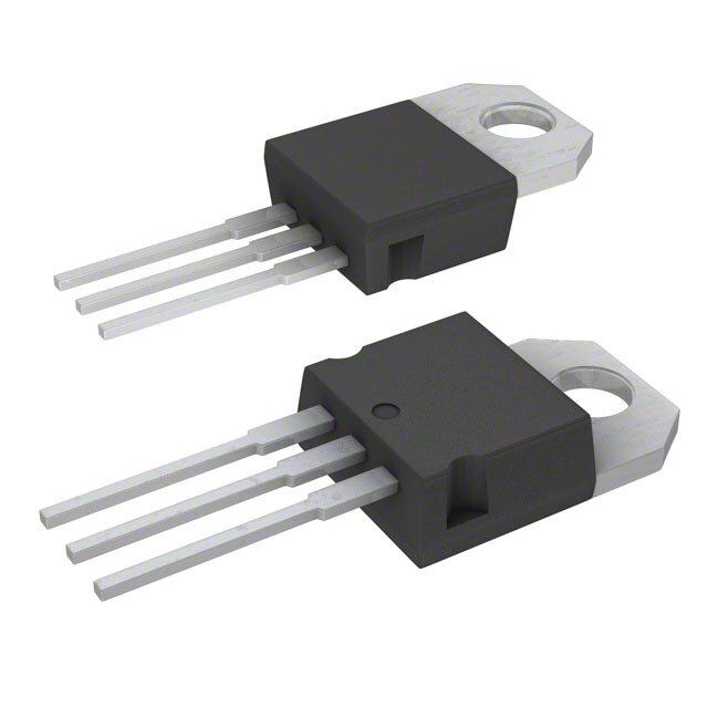
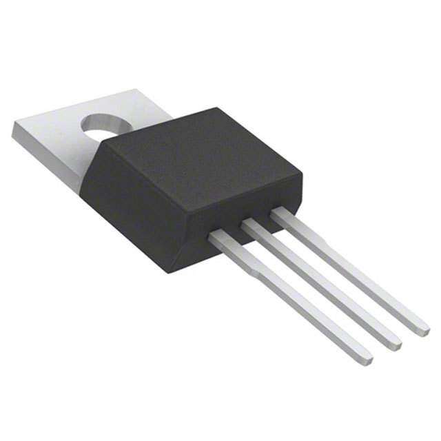
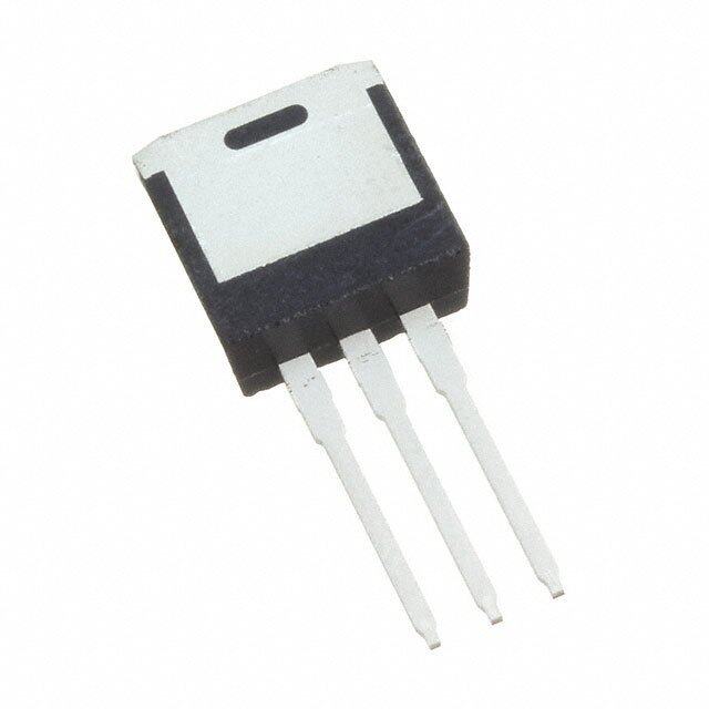
| 供应商器件封装 | TO-220AB |
| 其它名称 | 497-3187-5 |
| 其它有关文件 | http://www.st.com/web/catalog/sense_power/FM100/CL824/SC1164/PF64734?referrer=70071840 |
| 典型关闭延迟时间 | 25 ns |
| 功率-最大值 | 70W |
| 包装 | 管件 |
| 商标 | STMicroelectronics |
| 安装类型 | 通孔 |
| 安装风格 | Through Hole |
| 封装 | Tube |
| 封装/外壳 | TO-220-3 |
| 封装/箱体 | TO-220-3 |
| 工厂包装数量 | 50 |
| 晶体管极性 | N-Channel |
| 最大工作温度 | + 175 C |
| 最小工作温度 | - 55 C |
| 标准包装 | 50 |
| 正向跨导-最小值 | 20 S |
| 漏源极电压(Vdss) | 30V |
| 电流-连续漏极(Id)(25°C时) | 40A (Tc) |
| 系列 | STP40NF03L |
| 通道模式 | Enhancement |
| 配置 | Single |


PDF Datasheet 数据手册内容提取
STF40NF03L STP40NF03L Ω N-channel 30 V, 0.018 , 40 A TO-220, TO-220FP STripFET™ Power MOSFET Features Type V R max I DSS DS(on) D STF40NF03L 30 V 0.022 Ω 23 A STP40NF03L 30 V 0.022 Ω 40 A ■ Low threshold device 3 3 2 2 1 1 Application TO-220 TO-220FP ■ Switching applications Description This Power MOSFET is the latest development of STMicroelectronics unique "single feature size" Figure 1. Internal schematic diagram strip-based process. The resulting transistor shows extremely high packing density for low on- resistance, rugged avalanche characteristics and less critical alignment steps therefore a remarkable manufacturing reproducibility. Table 1. Device summary Order codes Marking Package Packaging STF40NF03L F40NF03L TO-220FP Tube STP40NF03L P40NF03L TO-220 Tube February 2010 Doc ID 6794 Rev 8 1/14 www.st.com 14
Contents STF40NF03L, STP40NF03L Contents 1 Electrical ratings . . . . . . . . . . . . . . . . . . . . . . . . . . . . . . . . . . . . . . . . . . . . 3 2 Electrical characteristics . . . . . . . . . . . . . . . . . . . . . . . . . . . . . . . . . . . . . 4 2.1 Electrical characteristics (curves) . . . . . . . . . . . . . . . . . . . . . . . . . . . . . 6 3 Test circuits . . . . . . . . . . . . . . . . . . . . . . . . . . . . . . . . . . . . . . . . . . . . . . 9 4 Package mechanical data . . . . . . . . . . . . . . . . . . . . . . . . . . . . . . . . . . . . 10 5 Revision history . . . . . . . . . . . . . . . . . . . . . . . . . . . . . . . . . . . . . . . . . . . 13 2/14 Doc ID 6794 Rev 8
STF40NF03L, STP40NF03L Electrical ratings 1 Electrical ratings Table 2. Absolute maximum ratings Value Symbol Parameter Unit TO-220 TO-220FP V Drain-source voltage (V = 0) 30 V DS GS V Gate- source voltage ± 16 V GS I Drain current (continuous) at T = 25 °C 40 23 A D C I Drain current (continuous) at T = 100 °C 28 16 A D C I (1) Drain current (pulsed) 160 92 A DM P Total dissipation at T = 25 °C 70 25 W tot C Derating factor 0.46 W/°C Insulation withstand voltage (RMS) from VISO all three leads to external heat sink 2500 V (t=1 s;T =25 °C) C E (2) Single pulse avalanche energy 250 mJ AS T Storage temperature stg -55 to 175 °C T Max. operating junction temperature j 1. Pulse width limited by safe operating area. 2. Starting T = 25 °C, I = 20 A, V = 15 V j D DD Table 3. Thermal data Value Symbol Parameter Package Unit Typ. Max. TO-220 1.8 2.1 Rthj-c Thermal resistance junction-case °C/W TO-220FP 6 Thermal resistance junction-ambient Rthj-amb 62.5 °C/W max Maximum lead temperature for T 300 °C J soldering purpose Doc ID 6794 Rev 8 3/14
Electrical characteristics STF40NF03L, STP40NF03L 2 Electrical characteristics (T =25 °C unless otherwise specified) CASE Table 4. On/off states Symbol Parameter Test conditions Min. Typ. Max. Unit Drain-source V I = 250 µA, V =0 30 V (BR)DSS breakdown voltage D GS V = max ratings Zero gate voltage DS 1 µA I V = max ratings, DSS drain current (V = 0) DS 10 µA GS T = 125 °C C Gate-body leakage I V = ±16 V ±100 nA GSS current (V = 0) GS DS V Gate threshold voltage V = V , I = 250 µA 1 1.7 2.5 V GS(th) DS GS D R Static drain-source on VGS = 10 V, ID = 20 A 0.018 0.022 Ω DS(on) resistance V = 4.5 V, I = 20 A 0.028 0.035 Ω GS D Table 5. Dynamic Symbol Parameter Test conditions Min. Typ. Max. Unit Forward g (1) V = 10 V, I =20 A - 20 - S fs transconductance DS D Input capacitance C 770 pF Ciss Output capacitance VDS = 25 V, f = 1 MHz, - 255 - pF Coss Reverse transfer VGS = 0 60 pF rss capacitance t Turn-on delay time 14 ns d(on) V = 15 V, I = 20 A t Rise time DD D 80 ns r R =4.7 Ω V = 4.5 V - - t Turn-off delay time G GS 25 ns d(off) (see Figure16) t Fall time 16 ns f Q Total gate charge V = 15 V, I = 40 A, 10.5 15 nC g DD D Q Gate-source charge V = 4.5 V - 4 nC gs GS Q Gate-drain charge (see Figure17) 4.5 nC gd 1. Pulsed: Pulse duration = 300 µs, duty cycle 1.5%. 4/14 Doc ID 6794 Rev 8
STF40NF03L, STP40NF03L Electrical characteristics Table 6. Source drain diode Symbol Parameter Test conditions Min. Typ. Max. Unit Source-drain current I 40 A SD Source-drain current - I (1) 160 A SDM (pulsed) V (2) Forward on voltage I = 40 A, V = 0 - 1.5 V SD SD GS I = 40 A, t Reverse recovery time SD 34.5 ns rr di/dt = 100 A/µs, Q Reverse recovery charge - 30 nC rr V = 15 V, T = 150 °C I Reverse recovery current DD j 2 A RRM (see Figure18) 1. Pulse width limited by safe operating area. 2. Pulsed: Pulse duration = 300 µs, duty cycle 1.5% Doc ID 6794 Rev 8 5/14
Electrical characteristics STF40NF03L, STP40NF03L 2.1 Electrical characteristics (curves) Figure 2. Safe operating area for TO-220 Figure 3. Thermal impedance for TO-220 Figure 4. Safe operating area for TO-220FP Figure 5. Thermal impedance for TO-220FP ID AM03797v1 (A) 100 OpLiermaittieodn ibny tmhias x arReDaS i(osn) 100µs 10 1ms 10ms 1 Tj=175°C Tc=25°C Sinlge 0.1 pulse 0.01 0.1 1 10 VDS(V) Figure 6. Output characteristics Figure 7. Transfer characteristics 6/14 Doc ID 6794 Rev 8
STF40NF03L, STP40NF03L Electrical characteristics Figure 8. Transconductance Figure 9. Static drain-source on resistance Figure 10. Gate charge vs. gate-source voltage Figure 11. Capacitance variations Figure 12. Normalized gate threshold voltage Figure 13. Normalized on resistance vs. vs. temperature temperature Doc ID 6794 Rev 8 7/14
Electrical characteristics STF40NF03L, STP40NF03L Figure 14. Source-drain diode forward Figure 15. Normalized B vs. temperature VDSS characteristics 8/14 Doc ID 6794 Rev 8
STF40NF03L, STP40NF03L Test circuits 3 Test circuits Figure 16. Switching times test circuit for Figure 17. Gate charge test circuit resistive load Figure 18. Test circuit for inductive load Figure 19. Unclamped inductive load test switching and diode recovery times circuit Figure 20. Unclamped inductive waveform Figure 21. Switching time waveform Doc ID 6794 Rev 8 9/14
Package mechanical data STF40NF03L, STP40NF03L 4 Package mechanical data In order to meet environmental requirements, ST offers these devices in different grades of ECOPACK® packages, depending on their level of environmental compliance. ECOPACK® specifications, grade definitions and product status are available at: www.st.com. ECOPACK is an ST trademark. 10/14 Doc ID 6794 Rev 8
STF40NF03L, STP40NF03L Package mechanical data TO-220 mechanical data mm inch Dim Min Typ Max Min Typ Max A 4.40 4.60 0.173 0.181 b 0.61 0.88 0.024 0.034 b1 1.14 1.70 0.044 0.066 c 0.48 0.70 0.019 0.027 D 15.25 15.75 0.6 0.62 D1 1.27 0.050 E 10 10.40 0.393 0.409 e 2.40 2.70 0.094 0.106 e1 4.95 5.15 0.194 0.202 F 1.23 1.32 0.048 0.051 H1 6.20 6.60 0.244 0.256 J1 2.40 2.72 0.094 0.107 L 13 14 0.511 0.551 L1 3.50 3.93 0.137 0.154 L20 16.40 0.645 L30 28.90 1.137 ∅P 3.75 3.85 0.147 0.151 Q 2.65 2.95 0.104 0.116 Doc ID 6794 Rev 8 11/14
Package mechanical data STF40NF03L, STP40NF03L TO-220FP mechanical data mm Dim. Min. Typ. Max. A 4.4 4.6 B 2.5 2.7 D 2.5 2.75 E 0.45 0.7 F 0.75 1 F1 1.15 1.70 F2 1.15 1.5 G 4.95 5.2 G1 2.4 2.7 H 10 10.4 L2 16 L3 28.6 30.6 L4 9.8 10.6 L5 2.9 3.6 L6 15.9 16.4 L7 9 9.3 Dia 3 3.2 L7 E A B D Dia L5 L6 F1 F2 F H G G1 L2 L4 L3 7012510_Rev_J 12/14 Doc ID 6794 Rev 8
STF40NF03L, STP40NF03L Revision history 5 Revision history T able 7. Document revision history Date Revision Changes 09-Sep-2004 1 Preliminary version 21-Jun-2005 2 Complete version with curves 16-Aug-2006 3 New template, no content change 21-Feb-2007 4 Typo mistake on page 1 20-Nov-2008 5 Figure9: Static drain-source on resistance has been corrected. 14-Apr-2009 6 The device in TO-220FP has been added 03-Feb-2010 7 Updated Table3: Thermal data. 22-Feb-2010 8 Updated Table3: Thermal data. Doc ID 6794 Rev 8 13/14
STF40NF03L, STP40NF03L Please Read Carefully: Information in this document is provided solely in connection with ST products. STMicroelectronics NV and its subsidiaries (“ST”) reserve the right to make changes, corrections, modifications or improvements, to this document, and the products and services described herein at any time, without notice. All ST products are sold pursuant to ST’s terms and conditions of sale. Purchasers are solely responsible for the choice, selection and use of the ST products and services described herein, and ST assumes no liability whatsoever relating to the choice, selection or use of the ST products and services described herein. No license, express or implied, by estoppel or otherwise, to any intellectual property rights is granted under this document. If any part of this document refers to any third party products or services it shall not be deemed a license grant by ST for the use of such third party products or services, or any intellectual property contained therein or considered as a warranty covering the use in any manner whatsoever of such third party products or services or any intellectual property contained therein. UNLESS OTHERWISE SET FORTH IN ST’S TERMS AND CONDITIONS OF SALE ST DISCLAIMS ANY EXPRESS OR IMPLIED WARRANTY WITH RESPECT TO THE USE AND/OR SALE OF ST PRODUCTS INCLUDING WITHOUT LIMITATION IMPLIED WARRANTIES OF MERCHANTABILITY, FITNESS FOR A PARTICULAR PURPOSE (AND THEIR EQUIVALENTS UNDER THE LAWS OF ANY JURISDICTION), OR INFRINGEMENT OF ANY PATENT, COPYRIGHT OR OTHER INTELLECTUAL PROPERTY RIGHT. UNLESS EXPRESSLY APPROVED IN WRITING BY AN AUTHORIZED ST REPRESENTATIVE, ST PRODUCTS ARE NOT RECOMMENDED, AUTHORIZED OR WARRANTED FOR USE IN MILITARY, AIR CRAFT, SPACE, LIFE SAVING, OR LIFE SUSTAINING APPLICATIONS, NOR IN PRODUCTS OR SYSTEMS WHERE FAILURE OR MALFUNCTION MAY RESULT IN PERSONAL INJURY, DEATH, OR SEVERE PROPERTY OR ENVIRONMENTAL DAMAGE. ST PRODUCTS WHICH ARE NOT SPECIFIED AS "AUTOMOTIVE GRADE" MAY ONLY BE USED IN AUTOMOTIVE APPLICATIONS AT USER’S OWN RISK. Resale of ST products with provisions different from the statements and/or technical features set forth in this document shall immediately void any warranty granted by ST for the ST product or service described herein and shall not create or extend in any manner whatsoever, any liability of ST. ST and the ST logo are trademarks or registered trademarks of ST in various countries. Information in this document supersedes and replaces all information previously supplied. The ST logo is a registered trademark of STMicroelectronics. All other names are the property of their respective owners. © 2010 STMicroelectronics - All rights reserved STMicroelectronics group of companies Australia - Belgium - Brazil - Canada - China - Czech Republic - Finland - France - Germany - Hong Kong - India - Israel - Italy - Japan - Malaysia - Malta - Morocco - Philippines - Singapore - Spain - Sweden - Switzerland - United Kingdom - United States of America www.st.com 14/14 Doc ID 6794 Rev 8
Mouser Electronics Authorized Distributor Click to View Pricing, Inventory, Delivery & Lifecycle Information: S TMicroelectronics: STP40NF03L STF40NF03L