ICGOO在线商城 > 分立半导体产品 > 晶体管 - FET,MOSFET - 单 > RSD050N10TL

 Datasheet下载
- 型号: RSD050N10TL
- 制造商: ROHM Semiconductor
- 库位|库存: xxxx|xxxx
- 要求:
| 数量阶梯 | 香港交货 | 国内含税 |
| +xxxx | $xxxx | ¥xxxx |
查看当月历史价格
查看今年历史价格
RSD050N10TL产品简介:
ICGOO电子元器件商城为您提供RSD050N10TL由ROHM Semiconductor设计生产,在icgoo商城现货销售,并且可以通过原厂、代理商等渠道进行代购。 RSD050N10TL价格参考¥2.46-¥5.83。ROHM SemiconductorRSD050N10TL封装/规格:晶体管 - FET,MOSFET - 单, 表面贴装 N 沟道 100V 5A(Ta) 15W(Tc) CPT3。您可以下载RSD050N10TL参考资料、Datasheet数据手册功能说明书,资料中有RSD050N10TL 详细功能的应用电路图电压和使用方法及教程。
RSD050N10TL 是由 Rohm Semiconductor 生产的一款 N 沟道增强型 MOSFET(金属氧化物半导体场效应晶体管)。它属于晶体管 - FET,MOSFET - 单一类别,广泛应用于多种电力电子场景。以下是该型号的主要应用场景:

 1. 开关电源 (SMPS)
   - RSD050N10TL 的低导通电阻(Rds(on))和高击穿电压(100V)使其非常适合用于开关电源中的高频开关应用。
   - 常见于 DC-DC 转换器、AC-DC 转换器以及 PFC(功率因数校正)电路中。

 2. 电机驱动
   - 适用于小型直流电机或步进电机的驱动控制。
   - 在 H 桥电路中用作高低侧开关,实现电机的正转、反转和制动功能。

 3. 负载开关
   - 用于需要高效开关的负载控制场景,例如消费电子产品中的电池管理系统 (BMS)。
   - 提供快速开关能力和低功耗特性。

 4. 保护电路
   - 可用于过流保护、短路保护和过温保护电路中。
   - 其内置的热关断和过电流限制功能增强了系统的可靠性。

 5. 汽车电子
   - 在汽车电子领域,可用于车身控制模块 (BCM)、电动窗户、座椅调节等低压控制应用。
   - 符合车规级要求(如 AEC-Q101),确保在恶劣环境下稳定工作。

 6. 工业自动化
   - 应用于工业设备中的信号隔离、传感器接口和继电器替代方案。
   - 支持高效的工业通信模块设计。

 7. 便携式设备
   - 适用于智能手机、平板电脑和其他便携式设备的电源管理单元 (PMU)。
   - 提供小尺寸封装(如 TO-252 或 DPAK),节省空间并降低功耗。

 特性总结
- 击穿电压:100V
- 导通电阻:典型值低至几百毫欧
- 最大漏极电流:几十安培
- 封装形式:表面贴装或通孔封装

这些特性使得 RSD050N10TL 成为高性能、高可靠性的 MOSFET 选择,适用于各种需要高效功率转换和控制的应用场景。
| 参数 | 数值 |
| 产品目录 | |
| 描述 | MOSFET N-CH 100V 5A CPT3MOSFET TRANS MOSFET N-CH 100V 5A 3PIN CPT |
| 产品分类 | FET - 单分离式半导体 |
| FET功能 | 逻辑电平栅极,4V 驱动 |
| FET类型 | MOSFET N 通道,金属氧化物 |
| Id-ContinuousDrainCurrent | 5 A |
| Id-连续漏极电流 | 5 A |
| 品牌 | ROHM Semiconductor |
| 产品手册 | |
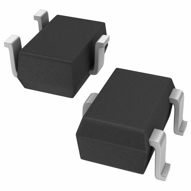
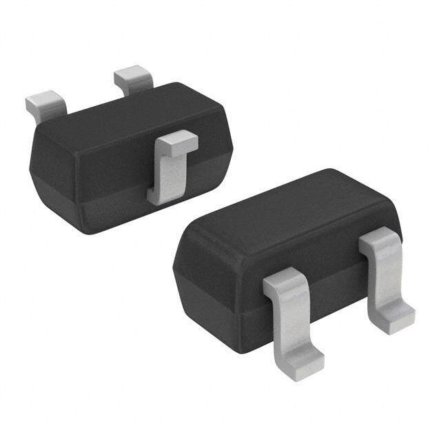
| 产品图片 |
|
| rohs | 符合RoHS无铅 / 符合限制有害物质指令(RoHS)规范要求 |
| 产品系列 | 晶体管,MOSFET,ROHM Semiconductor RSD050N10TL- |
| 数据手册 | 点击此处下载产品Datasheet点击此处下载产品Datasheet点击此处下载产品Datasheet点击此处下载产品Datasheet |
| 产品型号 | RSD050N10TL |
| Pd-PowerDissipation | 15 W |
| Pd-功率耗散 | 15 W |
| Qg-GateCharge | 14 nC |
| Qg-栅极电荷 | 14 nC |
| RdsOn-Drain-SourceResistance | 145 mOhms |
| RdsOn-漏源导通电阻 | 145 mOhms |
| Vds-Drain-SourceBreakdownVoltage | 100 V |
| Vds-漏源极击穿电压 | 100 V |
| Vgs-Gate-SourceBreakdownVoltage | 20 V |
| Vgs-栅源极击穿电压 | 20 V |
| Vgsth-Gate-SourceThresholdVoltage | 1 V to 2.5 V |
| Vgsth-栅源极阈值电压 | 1 V to 2.5 V |
| 上升时间 | 15 ns |
| 下降时间 | 15 ns |
| 不同Id时的Vgs(th)(最大值) | 2.5V @ 1mA |
| 不同Vds时的输入电容(Ciss) | 530pF @ 25V |
| 不同Vgs时的栅极电荷(Qg) | 14nC @ 10V |
| 不同 Id、Vgs时的 RdsOn(最大值) | 190 毫欧 @ 5A, 10V |
| 产品种类 | MOSFET |
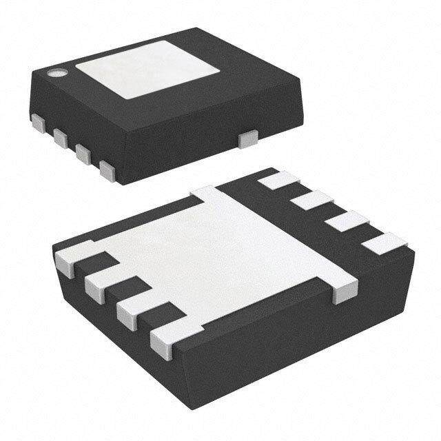
| 供应商器件封装 | CPT3 |
| 其它名称 | RSD050N10TLCT |
| 典型关闭延迟时间 | 45 ns |
| 功率-最大值 | 15W |
| 包装 | 剪切带 (CT) |
| 商标 | ROHM Semiconductor |
| 安装类型 | 表面贴装 |
| 安装风格 | SMD/SMT |
| 封装 | Reel |
| 封装/外壳 | TO-252-3,DPak(2 引线+接片),SC-63 |
| 封装/箱体 | CPT-3 |
| 工厂包装数量 | 2500 |
| 晶体管极性 | N-Channel |
| 最大工作温度 | + 150 C |
| 最小工作温度 | - 55 C |
| 标准包装 | 1 |
| 正向跨导-最小值 | 2.5 S |
| 漏源极电压(Vdss) | 100V |
| 电流-连续漏极(Id)(25°C时) | 5A (Ta) |
| 配置 | Single |


- 商务部:美国ITC正式对集成电路等产品启动337调查
- 曝三星4nm工艺存在良率问题 高通将骁龙8 Gen1或转产台积电
- 太阳诱电将投资9.5亿元在常州建新厂生产MLCC 预计2023年完工
- 英特尔发布欧洲新工厂建设计划 深化IDM 2.0 战略
- 台积电先进制程称霸业界 有大客户加持明年业绩稳了
- 达到5530亿美元!SIA预计今年全球半导体销售额将创下新高
- 英特尔拟将自动驾驶子公司Mobileye上市 估值或超500亿美元
- 三星加码芯片和SET,合并消费电子和移动部门,撤换高东真等 CEO
- 三星电子宣布重大人事变动 还合并消费电子和移动部门
- 海关总署:前11个月进口集成电路产品价值2.52万亿元 增长14.8%


PDF Datasheet 数据手册内容提取
4V Drive Nch MOSFET RSD050N10 Structure Dimensions (Unit : mm) r Silicon N-channel MOSFET o CPT3 (SC-63) 6.5 <SOT-428> 5.1 f 2.3 0.5 Features 1.5 1) Low on-resistance. d 23)) DFarisvte s cwiritccuhitins gc asnp ebeed .simple. e 0.9 5.5 1.59.5 3) Parallel use is easy. 0.75 2.5 d 0.9(1)2.3(2) (3)0.26.53 0.8Min.0.5 1.0 Applications Switching s n n e Packaging specifications Inner circuit g Package CPT3 m ∗1 Type Code TL i Basic ordering unit (pieces) 2500 s m (1) Gate ∗2 (2) Drain e (3) Source Absolute maximum ratings (T =25°C) o *1 ESD Protection Diode a D *2 Body Diode (1) (2) (3) Parameter Symbol Limits Unit c Drain-source voltage V 100 V DSS Gate-source voltage V 20 V GSS w e Continuous I 5.0 A Drain current D Pulsed I **11 20 A DP R Source current Continuous IeS 5.0 A (Body Diode) Pulsed I *1 20 A SP Power dissipation N P *2 15 W D t Channel temperature T 150 °C ch Range of sotorage temperature T 55 to +150 °C stg *1 Pw≦10s, Duty cycle≦1% N *2 Tc=25°C Thermal resistance Parameter Symbol Limits Unit Channel to Case R * 8.33 °C / W th (ch-c) * Tc=25C www.rohm.com ©2012 ROHM Co., Ltd. All rights reserved. 1/6 2012.02 - Rev.B
DataSheet RSD050N10 Electrical characteristics (T =25°C) a Parameter Symbol Min. Typ. Max. Unit Conditions Gate-source leakage I - - ±10 A V =±20V, V =0V GSS GS DS Drain-source breakdown voltage V 100 - - V I =1mA, V =0V (BR)DSS D GS Zero gate voltage drain current I - - 10 A V =100V, V =0V DSS DS GS Gate threshold voltage V 1.0 - 2.5 V V =10V, I =1mA GS (th) DS D - 135 190 I =5.0A, V =10V D GS r Static drain-source on-state * resistance RDS (on) - 142 200 m ID=5.0A, VGS=4.5V o - 145 205 I =5.0A, V =4.0V D GS Forward transfer admittance l Y l** 2.5 - - S I =5.0A, V =10V fs D DS f Input capacitance C - 530 - pF V =25V iss DS Output capacitance Coss - 50 - pF VGS=0V d Reverse transfer capacitance C - 30 - pF f=1MHz rss Turn-on delay time td(on)** - 10 - ns ID=2.5A,e VDD 50V Rise time tr ** - 15 - ns VGS=10V d Turn-off delay time td(off)** - 45 - ns RL=20 Fall time t ** - 15 - ns R =10 f G s n Total gate charge Q ** - 14 - nC V 50V g DD Gate-source charge Q ** - 1.7 - nC I =5.0A, n gs e D Gate-drain charge Qgd** - 3.0 - nC VGS=10V g *Pulsed m i s Body diode characteristics (Source-Drain) (T =25m °C) a Parameter Symbol Min. Typ. Max.eUnit Conditions Forward Voltage V * - - 1.2 V I =5.0A, V =0V SD s GS o D *Pulsed c w e R e N t o N www.rohm.com © 2012 ROHM Co., Ltd. All rights reserved. 2/6 2012.02 - Rev.B
DataSheet RSD050N10 Electrical characteristic curves (T =25C) a Fig.1 Typical Output Characteristics (Ⅰ) Fig.2 Typical Output Characteristics (Ⅱ) 5 5 V =10.0V GS V =2.5V VGS=10.0V VGS=4.0V GS 4 VGS=4.0V 4 VGS=3.0V VGS=3.0V A] r [ ent : I[A]D 3 VGS=2.5V Current : ID 3 o n Curr 2 Drain 2 f ai Dr d 1 1 Ta=25°C e Ta=25°C pulsed pulsed 0 0 0 0.2 0.4 0.6 0.8 1 0 2 4 6 8 10 d Drain-Source Voltage : VDS[V] Drain-Source Voltage : VDS[V] s n Fig.3 Static Drain-Source On-State Resistance vs. Drain Current Fig.4 Static Drain-Source On-State Resistance vs. Drain Current n 1000 e10000 V =10V GS Ta=25°C pulsed Static Drain-Source On-State ResistanceR[mΩ]DS(on) pulsed VVVcGGGSSS===441..005VVVo m m DStatic Drain-Source On-State ResistanceR[mΩ]DS(on) e1010000 sig TTTTaaaa====172-225555°°°CC°CC w 100 e 10 0.01 0.1 1 10 0.01 0.1 1 10 R Drain Current : I [A] Drain Current : ID[A] D e Fig.5 Static Drain-Source On-State Resistance vs. Drain Current Fig.6 Static Drain-Source On-State Resistance vs. Drain Current N 10000t 10000 NDrain-Source On-State ResistanceR[mΩ]DS(on) o1010000 VpuGlSs=e4d.5V TTTTaaaa====172-225555°°°CC°CC Drain-Source On-State ResistanceR[mΩ]DS(on) 1010000 VpuGlSs=e4dV TTTTaaaa====172-225555°°°CC°CC Static Static 10 10 0.01 0.1 1 10 0.01 0.1 1 10 Drain Current : ID[A] Drain Current : ID[A] www.rohm.com © 2012 ROHM Co., Ltd. All rights reserved. 3/6 2012.02 - Rev.B
DataSheet RSD050N10 Fig.7 Forward Transfer Admittance vs. Drain Current Fig.8 Typical Transfer Characteristics 100 10 VpuDlSs=e1d0V VpuDlSs=e1d0V 10 1 e r c n ard Transfer AdmittaY[S]fs 1 TTTTaaaa====172-225555°°°CC°CC Drain Currnt : I[A]D 0.1 TTTTaaaa====172-225555°°°CC°CC fo w or 0.1 0.01 d F e 0.01 0.001 0.01 0.1 1 10 0.0 d0.5 1.0 1.5 2.0 2.5 3.0 3.5 Drain Current : ID[A] Gate-Source Voltage : VGS[V] s n Fig.9 Source Current vs. Source-Drain Voltage Fig.10 Static Drain-Source On-State Resistance vs. Gate-Source Voltage n 10 e 500 VGS=0V Ta=25°C pulsed pulsed g m e Ta=125°C anc 400 Ta=75°C sist i Source Current : Is [A] 0.11 TTaa==o2-255°°CC m D ain-Source On-State ReR[mΩ]DS(on)e230000 s IIDD==25..50AA Dr c c ati 100 St w e 0.01 0 0.0 0.5 1.0 1.5 0 2 4 6 8 10 RSource-Drain Voltage : VSD[V] Gate-Source Voltage : VGS[V] e Fig.11 Switching Characteristics Fig.12 Dynamic Input Characteristics N 10000t 10 VDD≒50V Ta=25°C o VGS=10V VDD=50V RTaG==2150°ΩC 8 IPDu=l5sAed N 1000 Pulsed V] tf [GS me : t [ns] 100 td(off) oltage : V 6 Switching Ti 10 td(on) Gate-Source V 4 2 t r 1 0 0.01 0.1 1 10 0 5 10 15 20 Drain Current : ID[A] Total Gate Charge : Qg [nC] www.rohm.com © 2012 ROHM Co., Ltd. All rights reserved. 4/6 2012.02 - Rev.B
DataSheet RSD050N10 Fig.13 Typical Capacitance vs. Drain-Source Voltage Fig.14 Maximum Safe Operating Area 10000 100 Ta=25°C Ois pliemraitteiodn b iyn Rthis are(Va = 10V) f=1MHz DS(on) GS V =0V GS 1000 10 r citance : C [pF] 100 CCisosss Current : I[ A ]D 1 fPWo= 100μs a Cap Drain PW= 1ms 10 Crss 0.1 Ta=25°C d PW= 10ms Single Pulse Mounted on a ceramic board. DC (30mm ×30mme ×0.8mm) Operation 1 0.01 0.01 0.1 1 10 100 1000 0.1 1 10 100 1000 d Drain-Source Voltage : VDS[V] Drain-Source Voltage : VDS[ V ] s n Fig.15 Normalized Transient Thermal Resistance v.s. Pulse Width n 10 e Tc=25°C Single Pulse g ()t m r nce : RRtthh((cchh--aa))=(t8)=.3r(3t)°×C/RWth(ch-a) i esista 1 m s R al erm e h T sient 0.1 o D n a Tr d c e aliz m Nor e w 0.01 0.0001 0.001 0.01 0.1 1 10 100 1000 R Pulse width : Pw (s) e N t o N www.rohm.com © 2012 ROHM Co., Ltd. All rights reserved. 5/6 2012.02 - Rev.B
DataSheet RSD050N10 Measurement circuits Pulse width VGS ID VDS 50% 90% 50% RL VGS 10% VDS D.U.T. 10% 10% RG VDD 90% 90% r td(on) tr td(off) tf o ton toff Fig.1-1 Switching time measurement circuit Fig.1-2 Switching waveforms f VG VGS ID d VDS Qg RL VGS e IG(Const.) D.U.T. Qgs Qgd VDD d Chnarge s Fig.2-1 Gate charge measurement circuit Fig.2-2 Gate Charge Waveform n e g m i s m e o D c w e R e N t o N www.rohm.com © 2012 ROHM Co., Ltd. All rights reserved. 6/6 2012.02 - Rev.B
Notice Notes No copying or reproduction of this document, in part or in whole, is permitted without the consent of ROHM Co.,Ltd. r The content specified herein is subject to change for improvement without notice. o The content specified herein is for the purpose of introducing ROHM's products (hereinafter "Products"). If you wish to use any such Product, please be sure to refer to the specificatiofns, which can be obtained from ROHM upon request. Examples of application circuits, circuit constants and any other information contaidned herein illustrate the standard usage and operations of the Products. The peripheral conditions must be taken into account when designing circuits for mass production. e Great care was taken in ensuring the accuracy of the information specified in this document. However, should you incur any damage arising from any inaccuradcy or misprint of such information, ROHM shall bear no responsibility for such damage. s n The technical information specified herein is intended only to show the typical functions of and examples of application circuits for the Products. ROHM does not grant you, explicitly or n implicitly, any license to use or exercise intellectual propeerty or other rights held by ROHM and other parties. ROHM shall bear no responsibility whatsoever for any dispute arising from the use of such technical information. g m The Products specified in this document are intended to be used with general-use electronic equipment or devices (such as audio visual equipment, office-automiation equipment, commu- nication devices, electronic appliances and amusement devices).s m The Products specified in this document are not designed to be radiation tolerant. e While ROHM always makes efforts to enhance the quality and reliability of its Products, a o Product may fail or malfunction for a variety of reasoDns. Please be sure to imcplement in your equipment using the Products safety measures to guard against the possibility of physical injury, fir e or any other damage caused in the event of the failure of any Product, such as derating, redundancy, fire control and fail-safe designs. ROHM w shall bear no eresponsibility whatsoever for your use of any Product outside of the prescribed scope or not in accordance with the instruction manual. R The Products are not designeed or manufactured to be used with any equipment, device or system which requires an extremely high level of reliability the failure or malfunction of which may result in a direct threat to human life or create a risk of human injury (such as a medical N instrument, transportation equipment, aerospace machinery, nuclear-reactor controller, fuel- t controller or other safety device). ROHM shall bear no responsibility in any way for use of any of the Products for the above special purposes. If a Product is intended to be used for any o such special purpose, please contact a ROHM sales representative before purchasing. N If you intend to export or ship overseas any Product or technology specified herein that may be controlled under the Foreign Exchange and the Foreign Trade Law, you will be required to obtain a license or permit under the Law. Thank you for your accessing to ROHM product informations. More detail product informations and catalogs are available, please contact us. ROHM Customer Support System http://www.rohm.com/contact/ www.rohm.com R1120A © 2012 ROHM Co., Ltd. All rights reserved.
Mouser Electronics Authorized Distributor Click to View Pricing, Inventory, Delivery & Lifecycle Information: R OHM Semiconductor: RSD050N10TL