ICGOO在线商城 > 分立半导体产品 > 晶体管 - FET,MOSFET - 单 > FDMA908PZ
 Datasheet下载
- 型号: FDMA908PZ
- 制造商: Fairchild Semiconductor
- 库位|库存: xxxx|xxxx
- 要求:
| 数量阶梯 | 香港交货 | 国内含税 |
| +xxxx | $xxxx | ¥xxxx |
查看当月历史价格
查看今年历史价格
FDMA908PZ产品简介:
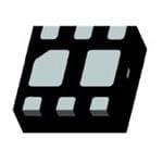
ICGOO电子元器件商城为您提供FDMA908PZ由Fairchild Semiconductor设计生产,在icgoo商城现货销售,并且可以通过原厂、代理商等渠道进行代购。 FDMA908PZ价格参考。Fairchild SemiconductorFDMA908PZ封装/规格:晶体管 - FET,MOSFET - 单, 表面贴装 P 沟道 12V 12A(Ta) 2.4W(Ta) 6-MicroFET(2x2)。您可以下载FDMA908PZ参考资料、Datasheet数据手册功能说明书,资料中有FDMA908PZ 详细功能的应用电路图电压和使用方法及教程。
ON Semiconductor的FDMA908PZ是一款N沟道增强型MOSFET(金属氧化物场效应晶体管),其应用场景广泛,尤其适用于需要高效、低功耗和高可靠性的电子设备。以下是该型号的主要应用场景:

1. 电源管理:FDMA908PZ常用于各种电源管理电路中,如开关电源(SMPS)、直流-直流转换器(DC-DC converters)和线性稳压器。其低导通电阻(Rds(on))特性有助于减少功率损耗,提高转换效率。

2. 电机控制:在小型电机驱动应用中,如风扇、泵和伺服电机等,FDMA908PZ可以作为开关元件,实现对电机速度和方向的精确控制。其快速开关特性和低热阻设计使其能够承受较大的电流波动。

3. 电池管理系统:在便携式设备和电动汽车的电池管理系统中,FDMA908PZ可用于保护电路,防止过充、过放和短路等情况。它还可以用于电池均衡电路,确保电池组中的每个单元都能均匀充电和放电。

4. 负载开关:在消费电子产品和工业控制系统中,FDMA908PZ可以用作负载开关,实现对不同负载的快速切换和保护。其低栅极电荷(Qg)特性使得开关速度更快,响应时间更短。

5. 信号调理与放大:在一些模拟电路中,FDMA908PZ可以用作信号调理和放大的关键元件,例如在音频放大器和传感器接口电路中。它的高输入阻抗和低噪声特性有助于提高信号质量。

6. 汽车电子:在汽车电子系统中,如车身控制模块(BCM)、电动助力转向(EPS)和照明控制系统中,FDMA908PZ可以提供可靠的开关功能,满足汽车级产品的严格要求。

7. 通信设备:在无线通信基站和有线通信设备中,FDMA908PZ可用于射频前端电路、功率放大器和滤波器等组件中,确保信号传输的稳定性和可靠性。

总之,FDMA908PZ凭借其优异的电气性能和可靠性,在多个领域有着广泛的应用前景,特别是在需要高效能和低功耗的场合。
| 参数 | 数值 |
| 产品目录 | |
| 描述 | MOSFET P-CH 12B 6QFNMOSFET -12V Single P-Channel PowerTrench MOSFET |
| 产品分类 | FET - 单分离式半导体 |
| FET功能 | 逻辑电平门 |
| FET类型 | MOSFET P 通道,金属氧化物 |
| Id-ContinuousDrainCurrent | - 12 A |
| Id-连续漏极电流 | - 12 A |
| 品牌 | Fairchild Semiconductor |
| 产品手册 | |
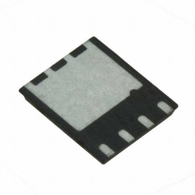
| 产品图片 |
|
| 产品系列 | 晶体管,MOSFET,Fairchild Semiconductor FDMA908PZPowerTrench® |
| 数据手册 | |
| 产品型号 | FDMA908PZ |
| Pd-PowerDissipation | 0.9 W, 2.4 W |
| Pd-功率耗散 | 900 mW, 2.4 W |
| RdsOn-Drain-SourceResistance | 13 mOhms |
| RdsOn-漏源导通电阻 | 13 mOhms |
| rohs | 无铅 / 符合限制有害物质指令(RoHS)规范要求 |
| Vds-Drain-SourceBreakdownVoltage | - 12 V |
| Vds-漏源极击穿电压 | - 12 V |
| Vgs-Gate-SourceBreakdownVoltage | 8 V |
| Vgs-栅源极击穿电压 | 8 V |
| Vgsth-Gate-SourceThresholdVoltage | - 0.6 V |
| Vgsth-栅源极阈值电压 | - 0.6 V |
| 上升时间 | 12 ns |
| 下降时间 | 71 ns |
| 不同Id时的Vgs(th)(最大值) | 1V @ 250µA |
| 不同Vds时的输入电容(Ciss) | 3957pF @ 6V |
| 不同Vgs时的栅极电荷(Qg) | 34nC @ 4.5V |
| 不同 Id、Vgs时的 RdsOn(最大值) | 12.5 毫欧 @ 12A, 4.5V |
| 产品种类 | MOSFET |
| 供应商器件封装 | MicroFET 2x2 |
| 其它名称 | FDMA908PZCT |
| 典型关闭延迟时间 | 131 ns |
| 功率-最大值 | 900mW |
| 包装 | 剪切带 (CT) |
| 单位重量 | 30 mg |
| 商标 | Fairchild Semiconductor |
| 安装类型 | 表面贴装 |
| 安装风格 | SMD/SMT |
| 导通电阻 | 13 mOhms |
| 封装 | Reel |
| 封装/外壳 | 6-WFDFN 裸露焊盘 |
| 封装/箱体 | MicroFET-6 2x2 |
| 工厂包装数量 | 3000 |
| 晶体管极性 | P-Channel |
| 最大工作温度 | + 150 C |
| 最小工作温度 | - 55 C |
| 标准包装 | 1 |
| 正向跨导-最小值 | 60 S |
| 汲极/源极击穿电压 | - 12 V |
| 漏极连续电流 | - 12 A |
| 漏源极电压(Vdss) | 12V |
| 电流-连续漏极(Id)(25°C时) | 12A (Ta) |
| 系列 | FDMA908 |
| 配置 | Single |


- 商务部:美国ITC正式对集成电路等产品启动337调查
- 曝三星4nm工艺存在良率问题 高通将骁龙8 Gen1或转产台积电
- 太阳诱电将投资9.5亿元在常州建新厂生产MLCC 预计2023年完工
- 英特尔发布欧洲新工厂建设计划 深化IDM 2.0 战略
- 台积电先进制程称霸业界 有大客户加持明年业绩稳了
- 达到5530亿美元!SIA预计今年全球半导体销售额将创下新高
- 英特尔拟将自动驾驶子公司Mobileye上市 估值或超500亿美元
- 三星加码芯片和SET,合并消费电子和移动部门,撤换高东真等 CEO
- 三星电子宣布重大人事变动 还合并消费电子和移动部门
- 海关总署:前11个月进口集成电路产品价值2.52万亿元 增长14.8%


PDF Datasheet 数据手册内容提取
Is Now Part of To learn more about ON Semiconductor, please visit our website at www.onsemi.com Please note: As part of the Fairchild Semiconductor integration, some of the Fairchild orderable part numbers will need to change in order to meet ON Semiconductor’s system requirements. Since the ON Semiconductor product management systems do not have the ability to manage part nomenclature that utilizes an underscore (_), the underscore (_) in the Fairchild part numbers will be changed to a dash (-). This document may contain device numbers with an underscore (_). Please check the ON Semiconductor website to verify the updated device numbers. The most current and up-to-date ordering information can be found at www.onsemi.com. Please email any questions regarding the system integration to Fairchild_questions@onsemi.com. ON Semiconductor and the ON Semiconductor logo are trademarks of Semiconductor Components Industries, LLC dba ON Semiconductor or its subsidiaries in the United States and/or other countries. ON Semiconductor owns the rights to a number of patents, trademarks, copyrights, trade secrets, and other intellectual property. A listing of ON Semiconductor’s product/patent coverage may be accessed at www.onsemi.com/site/pdf/Patent-Marking.pdf. ON Semiconductor reserves the right to make changes without further notice to any products herein. ON Semiconductor makes no warranty, representation or guarantee regarding the suitability of its products for any particular purpose, nor does ON Semiconductor assume any liability arising out of the application or use of any product or circuit, and specifically disclaims any and all liability, including without limitation special, consequential or incidental damages. Buyer is responsible for its products and applications using ON Semiconductor products, including compliance with all laws, regulations and safety requirements or standards, regardless of any support or applications information provided by ON Semiconductor. “Typical” parameters which may be provided in ON Semiconductor data sheets and/or specifications can and do vary in different applications and actual performance may vary over time. All operating parameters, including “Typicals” must be validated for each customer application by customer’s technical experts. ON Semiconductor does not convey any license under its patent rights nor the rights of others. ON Semiconductor products are not designed, intended, or authorized for use as a critical component in life support systems or any FDA Class 3 medical devices or medical devices with a same or similar classification in a foreign jurisdiction or any devices intended for implantation in the human body. Should Buyer purchase or use ON Semiconductor products for any such unintended or unauthorized application, Buyer shall indemnify and hold ON Semiconductor and its officers, employees, subsidiaries, affiliates, and distributors harmless against all claims, costs, damages, and expenses, and reasonable attorney fees arising out of, directly or indirectly, any claim of personal injury or death associated with such unintended or unauthorized use, even if such claim alleges that ON Semiconductor was negligent regarding the design or manufacture of the part. ON Semiconductor is an Equal Opportunity/Affirmative Action Employer. This literature is subject to all applicable copyright laws and is not for resale in any manner.
F D M A February 2014 9 0 8 FDMA908PZ P Z Single P-Channel PowerTrench® MOSFET S i n g -12 V, -12 A, 12.5 mΩ l e Features P - C (cid:132) Max r = 12.5 mΩ at V = -4.5 V, I = -12 A General Description h DS(on) GS D a (cid:132) Max r = 18 mΩ at V = -2.5 V, I = -10 A This device is designed specifically for battery charge or load n DS(on) GS D n switching in cellular handset and other ultraportable applications. (cid:132) Max r = 28 mΩ at V = -1.8 V, I = -8 A e DS(on) GS D It features a MOSFET with low on-state resistance and zener l (cid:132) Low Profile - 0.8 mm maximum in the new package MicroFET diode protection against ESD. The MicroFET 2X2 package P o 2x2 mm offers exceptional thermal performance for its physical size and w is well suited to linear mode applications. e (cid:132) HBM ESD protection level > 2.8 kV typical (Note 3) r T (cid:132) Free from halogenated compounds and antimony oxides r e n (cid:132) RoHS Compliant c h ® M O S Pin 1 D D G F E Bottom Drain Contact T D D Drain Source D D G S D D S MicroFET 2X2 (Bottom View) MOSFET Maximum Ratings TA = 25 °C unless otherwise noted Symbol Parameter Ratings Units V Drain to Source Voltage -12 V DS V Gate to Source Voltage ±8 V GS Drain Curre -Continuous T = 25 °C (Note 1a) -12 I A A D -Pulsed -40 Power Dissipation T = 25 °C (Note 1a) 2.4 P A W D Power Dissipation T = 25 °C (Note 1b) 0.9 A T , T Operating and Storage Junction Temperature Range -55 to +150 °C J STG Thermal Characteristics R Thermal Resistance, Junction to Ambient (Note 1a) 52 θJA °C/W R Thermal Resistance, Junction to Ambient (Note 1b) 145 θJA Package Marking and Ordering Information Device Marking Device Package Reel Size Tape Width Quantity 908 FDMA908PZ MicroFET 2X2 7 ” 12 mm 3000 units ©2013 Fairchild Semiconductor Corporation 1 www.fairchildsemi.com FDMA908PZ Rev.E3
F Electrical Characteristics D T = 25 °C unless otherwise noted J M Symbol Parameter Test Conditions Min Typ Max Units A 9 Off Characteristics 0 8 P BV Drain to Source Breakdown Voltage I = -250 μA, V = 0 V -12 V DSS D GS Z ΔBV Breakdown Voltage Temperature DSS I = -250 μA, referenced to 25 °C -10 mV/°C S ΔTJ Coefficient D in I Zero Gate Voltage Drain Current V = -9.6 V, V = 0 V -1 μA g DSS DS GS l I Gate to Source Leakage Current V = ±8 V, V = 0 V ±10 μA e GSS GS DS P On Characteristics -C h VGS(th) Gate to Source Threshold Voltage VGS = VDS, ID = -250 μA -0.4 -0.6 -1 V a ΔV Gate to Source Threshold Voltage n GS(th) I = -250 μA, referenced to 25 °C 2.8 mV/°C n ΔTJ Temperature Coefficient D e l V = -4.5 V, I = -12 A 10 12.5 GS D P V = -2.5 V, I = -10 A 13 18 o GS D w rDS(on) Static Drain to Source On Resistance VGS = -1.8 V, ID = -8 A 18 28 mΩ e V = -4.5 V, I = -12 A, r GS D 13 16 T TJ = 125 °C re g Forward Transconductance V = -5 V, I = -12 A 63 S n FS DD D c h Dynamic Characteristics ® C Input Capacitance 2638 3957 pF M iss C Output Capacitance VDS = -6 V, VGS = 0 V, 649 974 pF O oss f = 1 MHz S Crss Reverse Transfer Capacitance 602 903 pF F E Switching Characteristics T t Turn-On Delay Time 11 21 ns d(on) V = -6 V, I = -12 A, t Rise Time DD D 12 23 ns r V = -4.5 V, R = 6 Ω t Turn-Off Delay Time GS GEN 131 223 ns d(off) t Fall Time 71 121 ns f Qg Total Gate Charge VGS = -4.5 V, VDD = -6 V, 24 34 nC Q Gate to Source Charge I = -12 A 3.4 nC gs D Q Gate to Drain “Miller” Charge 5.3 nC gd Drain-Source Diode Characteristics V = 0 V, I = -2 A (Note 2) -0.6 -1.2 V V Source to Drain Diode Forward Voltage GS S SD V = 0 V, I = -12 A (Note 2) -0.8 -1.2 V GS S t Reverse Recovery Time 26 42 ns rr I = -12 A, di/dt = 100 A/μs Q Reverse Recovery Charge F 8.5 17 nC rr NOTES: 1. RθJA is determined with the device mounted on a 1 in2 pad 2 oz copper pad on a 1.5 x 1.5 in. board of FR-4 material. RθJC is guaranteed by design while RθCA is determined by the user's board design. a. 52 °C/W when mounted b. 145 °C/W when mounted on a on a 1 in2 pad of 2 oz copper. minimum pad of 2 oz copper. GDDSS FSFS GDDSS FSFS 2. Pulse Test: Pulse Width < 300 μs, Duty cycle < 2.0%. 3. The diode connected between the gate and source serves only as protection against ESD. No gate overvoltage rating is implied. ©2013 Fairchild Semiconductor Corporation 2 www.fairchildsemi.com FDMA908PZ Rev.E3
F D Typical Characteristics M T = 25 °C unless otherwise noted J A 9 40 3 0 8 VGS = -4.5 V NCE PZ A) 30 VGS = -3 V STA VGS = -1.5 V S T ( VGS = -2.5 V ESI 2 in CURREN 20 VGS = -1.8 V MALIZEDCE ON-R VGS = -1.8 V VGS = -2.5 V VGS = -3 V gle P -I, DRAIN D 10 VGS = -1.5 V PDUULTSYE C DYUCRLEA T=I O0.N5 %= 8M0A μXs NORRAIN TO SOUR 1 PDUULTSYE C DYUCRLEA T=I O0.N5 %= 8M0A μXs VGS = -4.5 V -Channe D 0 0 l 0.0 0.5 1.0 1.5 2.0 0 10 20 30 40 P -VDS, DRAIN TO SO URCE VOLTAGE (V) -ID, DRAIN CURR ENT (A) ow e Figure 1. On-Region Characteristics Figure 2. Normalized On- Resistance r T vs Drain Current and Gate Voltage r e n 60 c NORMALIZED O SOURCE ON-RESISTANCE 011111......901234 IVDG =S =-1 2-4A.5V rDRAIN TO ,DS(on)()URCE ON-RESISTANCE mΩ2400 TPDJUU =LT 1SY2E C5 D YoIDUCC =RL EA-1 T=2I O 0A.N5 %= 8M0A μXs h MOSFET® T O N 0.8 S TJ = 25 oC AI R 0 D 0.7 1.0 1.5 2.0 2.5 3.0 3.5 4.0 4.5 -75 -50 -25 0 25 50 75 100 125 150 TJ, JUNCTION TEM PERATURE (oC) -VGS, GATE TO SOURCE VOLTAGE (V) Figure 3. Normalized On- Resistance Figure 4. On-Resistance vs Gate to vs Junction Temperature Source Voltage 40 100 PULSE DURATION = 80 μs A) VGS = 0 V DUTY CYCLE = 0.5% MAX T ( EN 10 A) 30 R URRENT ( 20 VDS = -5 V TJ = 150 oC RAIN CUR 1 TJ = 150 oC N C TJ = 25 oC E D 0.1 TJ = 25 oC AI RS R E D 10 V -I, D TJ = -55 oC , RES0.01 TJ = -55 oC -I 0 0.001 0.0 0.5 1.0 1.5 2.0 0.0 0.4 0.8 1.2 -VGS, GATE TO SO URCE VOLTAGE (V) -VSD, BODY DIODE FO RWARD VOLTAGE (V) Figure 5. Transfer Characteristics Figure 6. Source to Drain Diode Forward Voltage vs Source Current ©2013 Fairchild Semiconductor Corporation 3 www.fairchildsemi.com FDMA908PZ Rev.E3
F D Typical Characteristics M T = 25 °C unless otherwise noted J A 9 4.5 5000 08 V) P E ( ID = -12A Ciss Z G OLTA3.0 VDD = -4V pF) Sin CE V VDD = -6V NCE ( gle O SOUR1.5 VDD = -8V PACITA1000 Coss P-C T A h TE C f = 1 MHz Crss a GA VGS = 0 V nn , S e -VG0.00 5 10 15 20 25 3000.1 1 10 20 l P Qg, GATE CH ARGE (nC) -VDS, DRAIN TO SOU RCE VOLTAGE (V) ow e Figure 7. Gate Charge Characteristics Figure 8. Capacitance vs Drain rT to Source Voltage r e n 10-3 60 c h GE CURRENT (A) 111000---654 VDS = 0 V TJ = 125 oC URRENT (A) 101 THIS AREA IS 110 m mss MOSFE® , -IGATE LEAKAg 111000---987 TJ = 25 oC -I, DRAIN CD 0.1 STTRLJAIθINM J ==AGI T M2=LE5 AE1 DXo 4PC 5BRU oYALC STr/DWEESD(on) CMUERAVSEU RBEEDN TD ATTOA 11D100 Cs0 s ms T 10-10 0.01 0 5 10 15 0.01 0.1 1 10 50 -VGS, GATE TO SOURCE VOLTAGE (V) -VDS, DRAIN to SOU RCE VOLTAGE (V) Figure 9. Gate Leakage Current Figure 10. Gate Leakage Current vs Gate to Source Voltage vs Gate to Source Voltage 100 SINGLE PULSE R (W) RθJA = 145 oC/W OWE 10 TA = 25 oC P T N E NSI A R T 1 K A E P , K) P P( 0.1 10-3 10-2 10-1 1 10 100 1000 t, PULSE WIDTH (s ec) Figure 11. Single Pulse Maximum Power Dissipation ©2013 Fairchild Semiconductor Corporation 4 www.fairchildsemi.com FDMA908PZ Rev.E3
F D Typical Characteristics M T = 25 °C unless otherwise noted J A 2 9 0 DUTY CYCLE-DESCENDING ORDER 8 1 P Z AL D = 00..25 S LIZED THERM ZEDANCE,JAθ0.1 0000....1000521 PDM t1 ingle P- NORMAIMP SRIθNJAG =L E1 4P5U oLCS/EW NDOUTTYE SF:ACTOR: D = t1/t2 t2 Chan (Note 1b) PEAK TJ = PDM x ZθJA x RθJA + TA n e l 0.01 P 10-3 10-2 10-1 1 10 100 1000 o t, RECTANGULAR PULSE DURATION (sec) w Figure 12. Junction-to-Ambient Transient Thermal Response Curve e r T r e n c h ® M O S F E T ©2013 Fairchild Semiconductor Corporation 5 www.fairchildsemi.com FDMA908PZ Rev.E3
2.05 A 0.05 C (0.20) B (0.45) 2X 1.00 6 5 4 2.05 2.30 1.05 0.66 1.35 0.05 C 0.475(6X) PIN1LOCATION 2X 1 2 3 TOPVIEW 0.65 0.40(6X) RECOMMENDEDLANDPATTERN (cid:19)(cid:17)(cid:27)(cid:3)(cid:147)(cid:19)(cid:17)(cid:19)(cid:24) 0.10 C (cid:19)(cid:17)(cid:21)(cid:19)(cid:147)(cid:19)(cid:17)(cid:19)(cid:24) Pin Function 0.08 C 1 Drain 2 Drain (cid:19)(cid:17)(cid:19)(cid:21)(cid:24)(cid:147)(cid:17)(cid:19)(cid:21)(cid:24) C 3 Gate SEATING SIDEVIEW 4 Source PLANE 5 Drain 6 Drain 7 Drain 8 Source (cid:21)(cid:17)(cid:19)(cid:24)(cid:147)(cid:19)(cid:17)(cid:19)(cid:24) (cid:19)(cid:17)(cid:28)(cid:19)(cid:147)(cid:19)(cid:17)(cid:20)(cid:19) (0.200)4X NOTES: (0.15) PIN1IDENT (0.50) A.PACKAGEDOESNOTCONFORMTO 1 2 3 (0.30) ANYJEDECSTANDARD. (cid:19)(cid:17)(cid:25)(cid:20)(cid:147)(cid:19)(cid:17)(cid:19)(cid:24) B.DIMENSIONSAREINMILLIMETERS. (cid:19)(cid:17)(cid:21)(cid:25)(cid:24)(cid:147)(cid:19)(cid:17)(cid:19)(cid:25)(cid:24) C.DIMENSIONSANDTOLERANCESPER (6X) ASMEY14.5M,2009. (cid:20)(cid:17)(cid:19)(cid:19)(cid:147)(cid:19)(cid:17)(cid:19)(cid:24) (0.50) 7 8 D.LANDPATTERNRECOMMENDATIONIS (cid:21)(cid:17)(cid:19)(cid:24)(cid:147)(cid:19)(cid:17)(cid:19)(cid:24) EXISTINGINDUSTRYLANDPATTERN. E.DRAWINGFILENAME:MKT-FDMA908Prev1. 6 5 4 F.REFERENCEDRAWINGNO:MKT-MLP06Prev1. (cid:19)(cid:17)(cid:22)(cid:19)(cid:147)(cid:19)(cid:17)(cid:19)(cid:24)(cid:11)(cid:25)(cid:59)(cid:12) 0.65 0.10 C A B 1.30 0.05 C BOTTOMVIEW
ON Semiconductor and are trademarks of Semiconductor Components Industries, LLC dba ON Semiconductor or its subsidiaries in the United States and/or other countries. ON Semiconductor owns the rights to a number of patents, trademarks, copyrights, trade secrets, and other intellectual property. A listing of ON Semiconductor’s product/patent coverage may be accessed at www.onsemi.com/site/pdf/Patent−Marking.pdf. ON Semiconductor reserves the right to make changes without further notice to any products herein. ON Semiconductor makes no warranty, representation or guarantee regarding the suitability of its products for any particular purpose, nor does ON Semiconductor assume any liability arising out of the application or use of any product or circuit, and specifically disclaims any and all liability, including without limitation special, consequential or incidental damages. Buyer is responsible for its products and applications using ON Semiconductor products, including compliance with all laws, regulations and safety requirements or standards, regardless of any support or applications information provided by ON Semiconductor. “Typical” parameters which may be provided in ON Semiconductor data sheets and/or specifications can and do vary in different applications and actual performance may vary over time. All operating parameters, including “Typicals” must be validated for each customer application by customer’s technical experts. ON Semiconductor does not convey any license under its patent rights nor the rights of others. ON Semiconductor products are not designed, intended, or authorized for use as a critical component in life support systems or any FDA Class 3 medical devices or medical devices with a same or similar classification in a foreign jurisdiction or any devices intended for implantation in the human body. Should Buyer purchase or use ON Semiconductor products for any such unintended or unauthorized application, Buyer shall indemnify and hold ON Semiconductor and its officers, employees, subsidiaries, affiliates, and distributors harmless against all claims, costs, damages, and expenses, and reasonable attorney fees arising out of, directly or indirectly, any claim of personal injury or death associated with such unintended or unauthorized use, even if such claim alleges that ON Semiconductor was negligent regarding the design or manufacture of the part. ON Semiconductor is an Equal Opportunity/Affirmative Action Employer. This literature is subject to all applicable copyright laws and is not for resale in any manner. PUBLICATION ORDERING INFORMATION LITERATURE FULFILLMENT: N. American Technical Support: 800−282−9855 Toll Free ON Semiconductor Website: www.onsemi.com Literature Distribution Center for ON Semiconductor USA/Canada 19521 E. 32nd Pkwy, Aurora, Colorado 80011 USA Europe, Middle East and Africa Technical Support: Order Literature: http://www.onsemi.com/orderlit Phone: 303−675−2175 or 800−344−3860 Toll Free USA/Canada Phone: 421 33 790 2910 Fax: 303−675−2176 or 800−344−3867 Toll Free USA/Canada Japan Customer Focus Center For additional information, please contact your local Email: orderlit@onsemi.com Phone: 81−3−5817−1050 Sales Representative © Semiconductor Components Industries, LLC www.onsemi.com www.onsemi.com 1
Mouser Electronics Authorized Distributor Click to View Pricing, Inventory, Delivery & Lifecycle Information: O N Semiconductor: FDMA908PZ