ICGOO在线商城 > 分立半导体产品 > 晶体管 - FET,MOSFET - 单 > BUZ32 H
 Datasheet下载
- 型号: BUZ32 H
- 制造商: Infineon
- 库位|库存: xxxx|xxxx
- 要求:
| 数量阶梯 | 香港交货 | 国内含税 |
| +xxxx | $xxxx | ¥xxxx |
查看当月历史价格
查看今年历史价格
BUZ32 H产品简介:
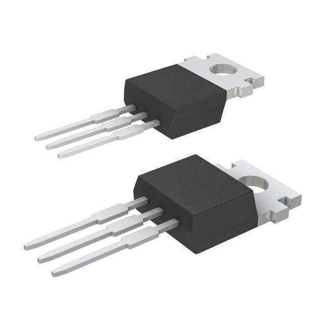
ICGOO电子元器件商城为您提供BUZ32 H由Infineon设计生产,在icgoo商城现货销售,并且可以通过原厂、代理商等渠道进行代购。 BUZ32 H价格参考。InfineonBUZ32 H封装/规格:晶体管 - FET,MOSFET - 单, 通孔 N 沟道 200V 9.5A(Tc) 75W(Tc) PG-TO220-3。您可以下载BUZ32 H参考资料、Datasheet数据手册功能说明书,资料中有BUZ32 H 详细功能的应用电路图电压和使用方法及教程。
Infineon Technologies(英飞凌科技)是一家全球领先的半导体制造商,其产品广泛应用于汽车、工业、能源和消费电子等领域。

型号为 BUZ32 H 的晶体管属于 MOSFET(金属氧化物半导体场效应晶体管) 类别,是单个N沟道功率MOSFET。该器件具有较高的电流和电压承受能力,适用于需要高效开关和功率控制的场景。

 主要应用场景包括:

1. 电源管理:BUZ32 H 常用于开关电源(SMPS)、DC-DC转换器和电源模块中,用于高效地控制电流流动,提高能源利用率。

2. 电机驱动:在工业自动化和电机控制系统中,作为功率开关用于控制直流电机或步进电机的启停与方向。

3. 汽车电子:用于汽车中的灯光控制、风扇驱动、电控系统等,满足汽车环境对可靠性和耐温性的要求。

4. 逆变器与UPS系统:在不间断电源(UPS)和逆变器中,用于将直流电转换为交流电,实现电力的稳定输出。

5. 充电设备:应用于电池充电器、电动车充电模块等,提供高效的功率控制。

该MOSFET具有低导通电阻、高耐压和良好热性能,适合中高功率应用场景,是工业与汽车电子中常用的功率开关元件。
| 参数 | 数值 |
| 产品目录 | |
| 描述 | MOSFET N-CH 200V 9.5A TO220-3MOSFET N-Channel 200V Transistor |
| 产品分类 | FET - 单分离式半导体 |
| FET功能 | 标准 |
| FET类型 | MOSFET N 通道,金属氧化物 |
| Id-ContinuousDrainCurrent | 9.5 A |
| Id-连续漏极电流 | 9.5 A |
| 品牌 | Infineon Technologies |
| 产品手册 | |
| 产品图片 |
|
| rohs | 符合RoHS无铅 / 符合限制有害物质指令(RoHS)规范要求 |
| 产品系列 | 晶体管,MOSFET,Infineon Technologies BUZ32 HSIPMOS® |
| 数据手册 | http://www.infineon.com/dgdl/Buz32H_Rev+2.4.pdf?folderId=db3a304325305e6d012596c6ca7b290a&fileId=db3a304325305e6d012597161028291a |
| 产品型号 | BUZ32 H |
| PCN过时产品 | |
| Pd-PowerDissipation | 75 W |
| Pd-功率耗散 | 75 W |
| RdsOn-Drain-SourceResistance | 400 mOhms |
| RdsOn-漏源导通电阻 | 400 mOhms |
| Vds-Drain-SourceBreakdownVoltage | 200 V |
| Vds-漏源极击穿电压 | 200 V |
| Vgs-Gate-SourceBreakdownVoltage | +/- 20 V |
| Vgs-栅源极击穿电压 | 20 V |
| 上升时间 | 40 nS |
| 下降时间 | 30 nS |
| 不同Id时的Vgs(th)(最大值) | 4V @ 1mA |
| 不同Vds时的输入电容(Ciss) | 530pF @ 25V |
| 不同Vgs时的栅极电荷(Qg) | - |
| 不同 Id、Vgs时的 RdsOn(最大值) | 400 毫欧 @ 6A,10V |
| 产品种类 | MOSFET |
| 供应商器件封装 | PG-TO220-3 |
| 其它名称 | BUZ32H |
| 典型关闭延迟时间 | 55 nS |
| 功率-最大值 | 75W |
| 包装 | 管件 |
| 商标 | Infineon Technologies |
| 商标名 | OptiMOS |
| 安装类型 | 通孔 |
| 安装风格 | Through Hole |
| 封装 | Tube |
| 封装/外壳 | TO-220-3 |
| 封装/箱体 | TO-220-3 |
| 工厂包装数量 | 500 |
| 晶体管极性 | N-Channel |
| 最大工作温度 | + 150 C |
| 最小工作温度 | - 55 C |
| 标准包装 | 500 |
| 漏源极电压(Vdss) | 200V |
| 电流-连续漏极(Id)(25°C时) | 9.5A (Tc) |
| 系列 | BUZ32 |
| 配置 | Single |
| 零件号别名 | BUZ32HXKSA1 SP000682998 |


- 商务部:美国ITC正式对集成电路等产品启动337调查
- 曝三星4nm工艺存在良率问题 高通将骁龙8 Gen1或转产台积电
- 太阳诱电将投资9.5亿元在常州建新厂生产MLCC 预计2023年完工
- 英特尔发布欧洲新工厂建设计划 深化IDM 2.0 战略
- 台积电先进制程称霸业界 有大客户加持明年业绩稳了
- 达到5530亿美元!SIA预计今年全球半导体销售额将创下新高
- 英特尔拟将自动驾驶子公司Mobileye上市 估值或超500亿美元
- 三星加码芯片和SET,合并消费电子和移动部门,撤换高东真等 CEO
- 三星电子宣布重大人事变动 还合并消费电子和移动部门
- 海关总署:前11个月进口集成电路产品价值2.52万亿元 增长14.8%


PDF Datasheet 数据手册内容提取
BUZ 32 H SIPMOS® Power Transistor • N channel • Enhancement mode • Avalanche-rated Pin 1 Pin 2 Pin 3 G D S Type V I R Package Pb-free DS D DS(on) Ω BUZ 32 H 200 V 9.5 A 0.4 PG-TO-220-3 Yes Maximum Ratings Parameter Symbol Values Unit Continuous drain current I A D T = 29 ˚C 9.5 C Pulsed drain current I Dpuls T = 25 ˚C 38 C Avalanche current,limited by T I 9.5 jmax AR Avalanche energy,periodic limited by T E 6.5 mJ jmax AR Avalanche energy, single pulse E AS Ω I = 9.5 A, V = 50 V, R = 25 D DD GS L = 2 mH, T = 25 ˚C 120 j ± Gate source voltage V 20 V GS Power dissipation P W tot T = 25 ˚C 75 C Operating temperature T -55 ... + 150 ˚C j Storage temperature T -55 ... + 150 stg ≤ Thermal resistance, chip case R 1.67 K/W thJC Thermal resistance, chip to ambient R 75 thJA DIN humidity category, DIN 40 040 E IEC climatic category, DIN IEC 68-1 55 / 150 / 56 Rev. 2.4 Page 1 2009-11-10
BUZ 32 H Electrical Characteristics, at T= 25˚C, unless otherwise specified j Parameter Symbol Values Unit min. typ. max. Static Characteristics Drain- source breakdown voltage V V (BR)DSS V = 0 V, I = 0.25 mA, T = 25 ˚C 200 - - GS D j Gate threshold voltage V GS(th) VGS=VDS, ID = 1 mA 2.1 3 4 Zero gate voltage drain current I µA DSS V = 200 V, V = 0 V, T = 25 ˚C - 0.1 1 DS GS j V = 200 V, V = 0 V, T = 125 ˚C - 10 100 DS GS j Gate-source leakage current I nA GSS V = 20 V, V = 0 V - 10 100 GS DS Ω Drain-Source on-resistance R DS(on) V = 10 V, I = 6 A - 0.3 0.4 GS D Rev. 2.4 Page 2 2009-11-10
BUZ 32 H Electrical Characteristics, at T= 25˚C, unless otherwise specified j Parameter Symbol Values Unit min. typ. max. Dynamic Characteristics Transconductance g S fs ≥ VDS 2 * ID * RDS(on)max, ID = 6 A 3 4.6 - Input capacitance C pF iss V = 0 V, V = 25 V, f = 1 MHz - 400 530 GS DS Output capacitance C oss V = 0 V, V = 25 V, f = 1 MHz - 85 130 GS DS Reverse transfer capacitance C rss V = 0 V, V = 25 V, f = 1 MHz - 45 70 GS DS Turn-on delay time t ns d(on) V = 30 V, V = 10 V, I = 3 A DD GS D Ω R = 50 - 10 15 GS Rise time t r V = 30 V, V = 10 V, I = 3 A DD GS D Ω R = 50 - 40 60 GS Turn-off delay time t d(off) V = 30 V, V = 10 V, I = 3 A DD GS D Ω R = 50 - 55 75 GS Fall time t f V = 30 V, V = 10 V, I = 3 A DD GS D Ω R = 50 - 30 40 GS Rev. 2.4 Page 3 2009-11-10
BUZ 32 H Electrical Characteristics, at T= 25˚C, unless otherwise specified j Parameter Symbol Values Unit min. typ. max. Reverse Diode Inverse diode continuous forward current I A S T = 25 ˚C - - 9.5 C Inverse diode direct current,pulsed I SM T = 25 ˚C - - 38 C Inverse diode forward voltage V V SD V = 0 V, I = 19 A - 1.4 1.7 GS F Reverse recovery time t ns rr VR = 100 V, IF=lS, diF/dt = 100 A/µs - 200 - Reverse recovery charge Q µC rr VR = 100 V, IF=lS, diF/dt = 100 A/µs - 0.6 - Rev. 2.4 Page 4 2009-11-10
BUZ 32 H Drain current Power dissipation ƒ ƒ I = (T ) P = (T ) D C tot C ≥ parameter: V 10 V GS 10 80 A W I 8 P D tot 60 7 50 6 5 40 4 30 3 20 2 10 1 0 0 0 20 40 60 80 100 120 ˚C 160 0 20 40 60 80 100 120 ˚C 160 T T C C Safe operating area Transient thermal impedanc e I = ƒ(V ) Z = ƒ(t) D DS th JC p parameter: D = 0.01, T = 25˚C parameter: D = t / T C p 10 2 10 1 tp = 7 .6 µ s K/W A 10 µs ID 10 1 R D S ( o n ) = V D S / I D 100 µs ZthJC 10 0 1 ms 10 -1 D = 0.50 0.20 10 0 10 ms 0.10 0.05 10 -2 0.02 DC 0.01 single pulse 10 -1 10 -3 10 0 10 1 10 2 V 10 -7 10 -6 10 -5 10 -4 10 -3 10 -2 10 -1s 10 0 V t DS p Rev. 2.4 Page 5 2009-11-10
BUZ 32 H Typ. output characteristic s Typ. drain-source on-resistanc e I = ƒ(V ) R = ƒ(I ) D DS DS (on) D parameter: t = 80 µs parameter: V p GS 22 1.3 Ptot = 75W Ω A l k j a b c d e f g h i 18 VGS [V] 1.1 ID h a 4.0 RDS (on) 1.0 b 4.5 16 c 5.0 0.9 g 14 d 5.5 0.8 e 6.0 f 12 f 6.5 0.7 g 7.0 10 e h 7.5 0.6 i 8.0 0.5 8 j 9.0 d k 10.0 0.4 i 6 j l 20.0 c 0.3 k 4 0.2 b VVGGSS [[VV]] == 2 0.1 aa b c d e f g h i j k a 44..50 5.0 5.5 6.0 6.5 7.0 7.5 8.0 9.0 10.0 20.0 0 0.0 0 2 4 6 8 10 12 V 16 0 4 8 12 16 A 22 V I DS D Typ. transfer characteristics ID = f (VGS) Typ. forward transconductance gfs = f (ID) parameter: tp = 80 µs parameter: tp = 80 µs, VDS≥2 x ID x RDS(on)max VDS≥2 x ID x RDS(on)max 13 6.0 A S 11 5.0 ID 10 gfs 4.5 9 4.0 8 3.5 7 3.0 6 2.5 5 2.0 4 1.5 3 2 1.0 1 0.5 0 0.0 0 1 2 3 4 5 6 7 8 V 10 0 2 4 6 8 A 12 V I GS D Rev. 2.4 Page 6 2009-11-10
BUZ 32 H Gate threshold voltage Drain-source on-resistanc e ƒ ƒ V = (T) R = (T) GS (th) j DS (on) j parameter: V = V , I = 1 mA parameter: I = 6 A, V = 10 V GS DS D D GS 1.3 4.6 Ω V 98% 4.0 1.1 V R GS(th) 3.6 DS (on)1.0 0.9 3.2 typ 0.8 2.8 0.7 2.4 2% 0.6 98% 2.0 0.5 1.6 typ 0.4 1.2 0.3 0.8 0.2 0.4 0.1 0.0 0.0 -60 -20 20 60 100 ˚C 160 -60 -20 20 60 100 ˚C 160 T Tj j Typ. capacitances Forward characteristics of reverse dio de C = f (VDS) I = ƒ(V ) F SD parameter:VGS = 0V, f = 1MHz parameter: Tj, tp = 80 µs 10 1 10 2 nF A C I F 10 0 10 1 C iss 10 -1 10 0 C T = 25 ˚C typ oss j T = 150 ˚C typ C j rss T = 25 ˚C (98%) j T = 150 ˚C (98%) j 10 -2 10 -1 0 5 10 15 20 25 30 V 40 0.0 0.4 0.8 1.2 1.6 2.0 2.4 V 3.0 V V DS SD Rev. 2.4 Page 7 2009-11-10
BUZ 32 H ƒ Avalanche energy E = (T) Typ. gate charge AS j parameter: I = 9.5 A, V = 50 V V = ƒ(Q ) D DD GS Gate Ω R = 25 , L = 2 mH parameter: I = 14 A GS D puls 130 16 mJ V 110 E V AS 100 GS 12 90 80 10 0,2 V 0,8 V DS max DS max 70 8 60 50 6 40 4 30 20 2 10 0 0 20 40 60 80 100 120 ˚C 160 0 4 8 12 16 20 24 28 32 nC 38 T Q j Gate Drain-source breakdown voltage ƒ V = (T) (BR)DSS j 240 V 230 V (BR)DSS 225 220 215 210 205 200 195 190 185 180 -60 -20 20 60 100 ˚C 160 T j Rev. 2.4 Page 8 2009-11-10
Published by Infineon Technologies AG 81726 Munich, Germany © 2009 Infineon Technologies AG All Rights Reserved. Legal Disclaimer The information given in this document shall in no event be regarded as a guarantee of conditions or characteristics. With respect to any examples or hints given herein, any typical values stated herein and/or any information regarding the application of the device, Infineon Technologies hereby disclaims any and all warranties and liabilities of any kind, including without limitation, warranties of non-infringement of intellectual property rights of any third party. Information For further information on technology, delivery terms and conditions and prices, please contact the nearest Infineon Technologies Office (www.infineon.com). Warnings Due to technical requirements, components may contain dangerous substances. For information on the types in question, please contact the nearest Infineon Technologies Office. Infineon Technologies components may be used in life-support devices or systems only with the express written approval of Infineon Technologies, if a failure of such components can reasonably be expected to cause the failure of that life-support device or system or to affect the safety or effectiveness of that device or system. Life support devices or systems are intended to be implanted in the human body or to support and/or maintain and sustain and/or protect human life. If they fail, it is reasonable to assume that the health of the user or other persons may be endangered.