ICGOO在线商城 > 分立半导体产品 > 晶体管 - FET,MOSFET - 单 > STW34NM60N
 Datasheet下载
- 型号: STW34NM60N
- 制造商: STMicroelectronics
- 库位|库存: xxxx|xxxx
- 要求:
| 数量阶梯 | 香港交货 | 国内含税 |
| +xxxx | $xxxx | ¥xxxx |
查看当月历史价格
查看今年历史价格
STW34NM60N产品简介:
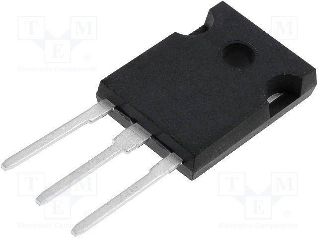
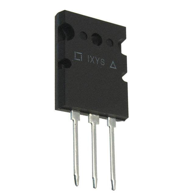
ICGOO电子元器件商城为您提供STW34NM60N由STMicroelectronics设计生产,在icgoo商城现货销售,并且可以通过原厂、代理商等渠道进行代购。 STW34NM60N价格参考。STMicroelectronicsSTW34NM60N封装/规格:晶体管 - FET,MOSFET - 单, 通孔 N 沟道 600V 29A(Tc) 250W(Tc) TO-247-3。您可以下载STW34NM60N参考资料、Datasheet数据手册功能说明书,资料中有STW34NM60N 详细功能的应用电路图电压和使用方法及教程。
STMicroelectronics的STW34NM60N是一款单通道MOSFET(金属-氧化物-半导体场效应晶体管),广泛应用于需要高效功率转换和开关操作的场景。以下是该型号的主要应用场景:

 1. 电源管理
   STW34NM60N常用于各种电源管理系统中,例如开关电源(SMPS)、直流-直流转换器(DC-DC Converter)等。其低导通电阻(Rds(on))特性有助于减少功率损耗,提高转换效率,特别适合于需要高能效的应用,如服务器、通信设备、工业自动化系统等。

 2. 电机驱动
   在电机驱动应用中,STW34NM60N可以作为功率开关,控制电机的启动、停止和速度调节。它能够承受较高的电流和电压波动,适用于无刷直流电机(BLDC)、步进电机和其他类型的电动机控制系统,常见于家用电器、电动工具和汽车电子等领域。

 3. 电池管理系统
   该MOSFET可用于电池管理系统的充放电控制电路中,确保电池在安全范围内工作。它可以在过流、过压或短路等异常情况下迅速切断电路,保护电池和相关设备免受损坏。此外,STW34NM60N的低导通电阻也有助于减少电池内部的发热,延长电池寿命。

 4. 太阳能逆变器
   在太阳能发电系统中,STW34NM60N可以用作逆变器中的关键组件,将光伏板产生的直流电转换为交流电并接入电网。其高效的开关性能和耐高压特性使其能够在恶劣环境下稳定工作,确保太阳能系统的可靠性和效率。

 5. 消费电子
   此外,STW34NM60N还适用于消费电子产品中的电源管理和信号切换功能,如笔记本电脑、平板电脑、智能手机等便携式设备。它可以有效降低功耗,延长电池续航时间,并提供快速响应的开关性能。

总之,STW34NM60N凭借其出色的电气性能和可靠性,成为多种电力电子应用的理想选择,特别是在需要高效功率转换和精确控制的场合。
| 参数 | 数值 |
| 产品目录 | |
| 描述 | MOSFET N-CH 600V 29A TO-247 |
| 产品分类 | FET - 单 |
| FET功能 | 标准 |
| FET类型 | MOSFET N 通道,金属氧化物 |
| 品牌 | STMicroelectronics |
| 数据手册 | |
| 产品图片 |
|
| 产品型号 | STW34NM60N |
| rohs | 无铅 / 符合限制有害物质指令(RoHS)规范要求 |
| 产品系列 | MDmesh™ II |
| 不同Id时的Vgs(th)(最大值) | 4V @ 250µA |
| 不同Vds时的输入电容(Ciss) | 2722pF @ 100V |
| 不同Vgs时的栅极电荷(Qg) | 80nC @ 10V |
| 不同 Id、Vgs时的 RdsOn(最大值) | 105 毫欧 @ 14.5A,10V |
| 供应商器件封装 | TO-247-3 |
| 其它名称 | 497-10975-5 |
| 其它有关文件 | http://www.st.com/web/catalog/sense_power/FM100/CL824/SC1167/PF250947?referrer=70071840 |
| 功率-最大值 | 210W |
| 包装 | 管件 |
| 安装类型 | 通孔 |
| 封装/外壳 | TO-247-3 |
| 标准包装 | 30 |
| 漏源极电压(Vdss) | 600V |
| 电流-连续漏极(Id)(25°C时) | 29A (Tc) |


- 商务部:美国ITC正式对集成电路等产品启动337调查
- 曝三星4nm工艺存在良率问题 高通将骁龙8 Gen1或转产台积电
- 太阳诱电将投资9.5亿元在常州建新厂生产MLCC 预计2023年完工
- 英特尔发布欧洲新工厂建设计划 深化IDM 2.0 战略
- 台积电先进制程称霸业界 有大客户加持明年业绩稳了
- 达到5530亿美元!SIA预计今年全球半导体销售额将创下新高
- 英特尔拟将自动驾驶子公司Mobileye上市 估值或超500亿美元
- 三星加码芯片和SET,合并消费电子和移动部门,撤换高东真等 CEO
- 三星电子宣布重大人事变动 还合并消费电子和移动部门
- 海关总署:前11个月进口集成电路产品价值2.52万亿元 增长14.8%


PDF Datasheet 数据手册内容提取
STW34NM60N Ω N-channel 600 V, 0.092 typ., 31.5 A MDmesh™ II Power MOSFETs in a TO-247 package Datasheet - production data Features Order code V R I P DSS DS(on) D TOT STW34NM60N 600 V 0.105 Ω 31.5 A 250 W • 100% avalanche tested • Low input capacitance and gate charge (cid:22) • Low gate input resistance (cid:21) (cid:20) Applications (cid:55)(cid:50)(cid:16)(cid:21)(cid:23)(cid:26) • Switching applications Description Figure 1. Internal schematic diagram This device is an N-channel Power MOSFET developed using the second generation of (cid:39)(cid:11)(cid:21)(cid:15)(cid:3)(cid:55)(cid:36)(cid:37)(cid:12) MDmesh™ technology. This revolutionary Power MOSFET associates a vertical structure to the company’s strip layout to yield one of the world’s lowest on-resistance and gate charge. It is therefore suitable for the most demanding high (cid:42)(cid:11)(cid:20)(cid:12) efficiency converters. (cid:54)(cid:11)(cid:22)(cid:12) (cid:36)(cid:48)(cid:19)(cid:20)(cid:23)(cid:26)(cid:24)(cid:89)(cid:20) Table 1. Device summary Order codes Marking Packages Packaging STW34NM60N 34NM60N TO-247 Tube March 2015 DocID027675 Rev 2 1/12 This is information on a product in full production. www.st.com 12
Contents STW34NM60N Contents 1 Electrical ratings . . . . . . . . . . . . . . . . . . . . . . . . . . . . . . . . . . . . . . . . . . . . 3 2 Electrical characteristics . . . . . . . . . . . . . . . . . . . . . . . . . . . . . . . . . . . . . 4 2.1 Electrical characteristics (curves) . . . . . . . . . . . . . . . . . . . . . . . . . . . . . . . . 6 3 Test circuits . . . . . . . . . . . . . . . . . . . . . . . . . . . . . . . . . . . . . . . . . . . . . . 8 4 Package information . . . . . . . . . . . . . . . . . . . . . . . . . . . . . . . . . . . . . . . . . 9 4.1 TO-247 package information . . . . . . . . . . . . . . . . . . . . . . . . . . . . . . . . . . . 9 5 Revision history . . . . . . . . . . . . . . . . . . . . . . . . . . . . . . . . . . . . . . . . . . . 11 2/12 DocID027675 Rev 2
STW34NM60N Electrical ratings 1 Electrical ratings Table 2. Absolute maximum ratings Symbol Parameter Value Unit V Drain-source voltage 600 V DS V Gate-source voltage ± 25 V GS I Drain current (continuous) at T = 25 °C 31.5 A D C I Drain current (continuous) at T = 100 °C 20 A D C I (1) Drain current (pulsed) 126 A DM P Total dissipation at T = 25 °C 250 W TOT C Max current during repetitive or single I pulse avalanche 7 A AR (pulse width limited by T ) jmax Single pulse avalanche energy E 345 mJ AS (starting T = 25 °C, I =I , V = 50 V) J D AS DD dv/dt (2) Peak diode recovery voltage slope 15 V/ns dv/dt(3) MOSFET dv/dt ruggedness 50 V/ns T Storage temperature -55 to 150 °C stg T Max. operating junction temperature 150 °C j 1. Pulse width limited by safe operating area. 2. I ≤ 31.5 A, di/dt ≤ 400 A/µs, V peak ≤ V , V = 80% V SD DS (BR)DSS DD (BR)DSS 3. V ≤ 480 V DS Table 3. Thermal data Symbol Parameter Value Unit R Thermal resistance junction-case max 0.5 thj-case °C/W R Thermal resistance junction-amb max 50 thj-amb DocID027675 Rev 2 3/12
Electrical characteristics STW34NM60N 2 Electrical characteristics (T = 25 °C unless otherwise specified). CASE Table 4. On/off states Symbol Parameter Test conditions Min. Typ. Max. Unit Drain-source breakdown V I = 1 mA 600 V (BR)DSS voltage (V = 0) D GS I Zero gate voltage drain VDS = 600 V 1 µA DSS current (VGS = 0) VDS = 600 V, Tc=125 °C 100 µA Gate body leakage current I V = ± 25 V ±100 nA GSS (V = 0) GS DS V Gate threshold voltage V = V , I = 250 µA 2 3 4 V GS(th) DS GS D Static drain-source on- R V = 10 V, I = 14.5 A 0.092 0.105 Ω DS(on) resistance GS D Table 5. Dynamic Symbol Parameter Test conditions Min. Typ. Max. Unit C Input capacitance - 2722 - pF iss C Output capacitance - 173 - pF oss V =100 V, f=1 MHz, V =0 DS GS Reverse transfer C - 1.75 - pF rss capacitance Equivalent capacitance time C (1) V = 0, V = 0 to 480 V - 458 - pF oss eq. related GS DS t Turn-on delay time - 18 - ns d(on) V = 300 V, I = 15.75 A, t Rise time DD D - 36 - ns r R =4.7 Ω, V =10 V G GS t Turn-off delay time - 104 - ns d(off) (see Figure19 and 14) t Fall time - 73 - ns f Q Total gate charge - 84 - nC g V = 480 V, I = 31.5 A DD D Q Gate-source charge V =10 V - 14 - nC gs GS (see Figure15) Q Gate-drain charge - 45 - nC gd f = 1 MHz, gate DC Bias=0 R Intrinsic gate resistance test signal level=20 mV - 2.9 - Ω G open drain 1. C . is defined as a constant equivalent capacitance giving the same charging time as C when V oss eq oss DS increases from 0 to 80% V DSS 4/12 DocID027675 Rev 2
STW34NM60N Electrical characteristics Table 6. Source drain diode Symbol Parameter Test conditions Min. Typ. Max. Unit I Source-drain current - 31.5 A SD I (1) Source-drain current (pulsed) - 126 A SDM V (2) Forward on voltage I = 31.5 A, V =0 - 1.6 V SD SD GS t Reverse recovery time - 412 ns rr I = 31.5 A, V = 60 V SD DD Q Reverse recovery charge di/dt = 100 A/µs, - 8 µC rr (see Figure16) I Reverse recovery current - 39 A RRM t Reverse recovery time I = 31.5 A,V = 60 V - 490 ns rr SD DD di/dt=100 A/µs, Q Reverse recovery charge - 10 µC rr T=150 °C j I Reverse recovery current (see Figure16) - 43 A RRM 1. Pulse width limited by safe operating area 2. Pulsed: Pulse duration = 300 µs, duty cycle 1.5%. DocID027675 Rev 2 5/12
Electrical characteristics STW34NM60N 2.1 Electrical characteristics (curves) Fig u re 2. Safe operating area Figure 3. Thermal impedance ID AM15707v1 (A) Tj=150°C Tc=25°C Single pulse 100 10µs 10 Operatmiitoen di n bty hism aaxr eRa DiSs(on) 110m0sµs Li 10ms 1 0.1 0.1 1 10 100 VDS(V) Figu r e 4. Output characteristics Figure 5. Transfer characteristics AM09020v1 AM09021v1 ID(A) ID(A) 80 VGS=10V 80 VDS=20V 70 70 60 60 6V 50 50 40 40 30 30 20 20 5V 10 10 0 0 0 5 10 15 20 25 30 VDS(V) 0 2 4 6 8 VGS(V) Figure 6. Gate charge vs gate-source voltage Figure 7. Static drain-source on-resistance V(VGS) AMV1D5S70(1Vv1) RDS((oΩn)) AM15702v1 VGS=10V 12 VDS VDD=480V ID=31.5A 500 0.096 10 400 0.094 8 300 0.092 6 200 0.09 4 2 100 0.088 0 0 0.086 0 20 40 60 80 Qg(nC) 0 5 10 15 20 25 30 ID(A) 6/12 DocID027675 Rev 2
STW34NM60N Electrical characteristics Figure 8. Capacitance variations Figure 9. Output capacitance stored energy C AM09024v1 Eoss AM09025v1 (pF) (µJ) 10000 Ciss 2 1000 Coss 100 1 10 Crss 1 0 0.1 1 10 100 VDS(V) 0 100 200 300 400 500 VDS(V) Figure 10. Normalized gate threshold voltage vs Figure 11. Normalized on-resistance vs temperature temperature VGS(th) AM09026v1 RDS(on) AM15703v1 (norm) ID=250µA (norm) 2.1 ID=14.5A 1.10 1.9 1.00 1.7 1.5 0.90 1.3 0.80 1.1 0.9 0.70 0.7 0.60 0.5 -50 -25 0 25 50 75 100 TJ(°C) -50 -25 0 25 50 75 100 TJ(°C) Figure 12. Normalized B vs temperature Figure 13. Source-drain diode forward VDSS characteristics VDS AM15704v1 VSD AM15705v1 (norm) ID=1mA (V) 1.07 1.4 TJ=-50°C 1.05 1.2 1.03 1 TJ=25°C 1.01 0.8 0.99 0.6 TJ=150°C 0.97 0.4 0.95 0.2 0.93 0 -50 -25 0 25 50 75 100 TJ(°C) 0 5 10 15 20 25 30 ISD(A) DocID027675 Rev 2 7/12
Test circuits STW34NM60N 3 Test circuits Figure 14. Switching times test circuit for Figure 15. Gate charge test circuit resistive load VDD 12V 47kΩ 1kΩ 100nF RL 2μ20F0 3μ.F3 VDD IG=CONST VD Vi=20V=VGMAX 100Ω D.U.T. VGS 2200 RG D.U.T. μF 2.7kΩ VG PW 47kΩ 1kΩ PW AM01468v1 AM01469v1 Figure 16. Test circuit for inductive load Figure 17. Unclamped inductive load test circuit switching and diode recovery times L A A A D FAST L=100μH VD G D.U.T. DIODE 2200 3.3 μF μF VDD S B 3.3 1000 B B μF μF 25Ω D VDD ID G RG S Vi D.U.T. Pw AM01470v1 AM01471v1 Figure 18. Unclamped inductive waveform Figure 19. Switching time waveform V(BR)DSS ton toff VD tdon tr tdoff tf 90% 90% IDM 10% ID 0 10% VDS VDD VDD 90% VGS AM01472v1 0 10% AM01473v1 8/12 DocID027675 Rev 2
STW34NM60N Package information 4 Package information In order to meet environmental requirements, ST offers these devices in different grades of ECOPACK® packages, depending on their level of environmental compliance. ECOPACK® specifications, grade definitions and product status are available at: www.st.com. ECOPACK® is an ST trademark. 4.1 TO-247 package information Figure 20. TO-247 drawing 0075325_H DocID027675 Rev 2 9/12
Package information STW34NM60N Table 7. TO-247 mechanical data mm. Dim. Min. Typ. Max. A 4.85 5.15 A1 2.20 2.60 b 1.0 1.40 b1 2.0 2.40 b2 3.0 3.40 c 0.40 0.80 D 19.85 20.15 E 15.45 15.75 e 5.30 5.45 5.60 L 14.20 14.80 L1 3.70 4.30 L2 18.50 ∅P 3.55 3.65 ∅R 4.50 5.50 S 5.30 5.50 5.70 10/12 DocID027675 Rev 2
STW34NM60N Revision history 5 Revision history Table 8. Document revision history Date Revision Changes 25-Mar-2015 1 Initial release. Updated Figure2: Safe operating area and Figure3: Thermal 30-Mar-2015 2 impedance. DocID027675 Rev 2 11/12
STW34NM60N IMPORTANT NOTICE – PLEASE READ CAREFULLY STMicroelectronics NV and its subsidiaries (“ST”) reserve the right to make changes, corrections, enhancements, modifications, and improvements to ST products and/or to this document at any time without notice. Purchasers should obtain the latest relevant information on ST products before placing orders. ST products are sold pursuant to ST’s terms and conditions of sale in place at the time of order acknowledgement. Purchasers are solely responsible for the choice, selection, and use of ST products and ST assumes no liability for application assistance or the design of Purchasers’ products. No license, express or implied, to any intellectual property right is granted by ST herein. Resale of ST products with provisions different from the information set forth herein shall void any warranty granted by ST for such product. ST and the ST logo are trademarks of ST. All other product or service names are the property of their respective owners. Information in this document supersedes and replaces information previously supplied in any prior versions of this document. © 2015 STMicroelectronics – All rights reserved 12/12 DocID027675 Rev 2
Mouser Electronics Authorized Distributor Click to View Pricing, Inventory, Delivery & Lifecycle Information: S TMicroelectronics: STW34NM60N