ICGOO在线商城 > 分立半导体产品 > 晶体管 - FET,MOSFET - 单 > SI1422DH-T1-GE3
 Datasheet下载
- 型号: SI1422DH-T1-GE3
- 制造商: Vishay
- 库位|库存: xxxx|xxxx
- 要求:
| 数量阶梯 | 香港交货 | 国内含税 |
| +xxxx | $xxxx | ¥xxxx |
查看当月历史价格
查看今年历史价格
SI1422DH-T1-GE3产品简介:
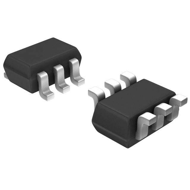
ICGOO电子元器件商城为您提供SI1422DH-T1-GE3由Vishay设计生产,在icgoo商城现货销售,并且可以通过原厂、代理商等渠道进行代购。 SI1422DH-T1-GE3价格参考。VishaySI1422DH-T1-GE3封装/规格:晶体管 - FET,MOSFET - 单, 表面贴装 N 沟道 12V 4A(Tc) 1.56W(Ta),2.8W(Tc) SC-70-6(SOT-363)。您可以下载SI1422DH-T1-GE3参考资料、Datasheet数据手册功能说明书,资料中有SI1422DH-T1-GE3 详细功能的应用电路图电压和使用方法及教程。
Vishay Siliconix 的 SI1422DH-T1-GE3 是一款P沟道增强型MOSFET,采用1.2mm × 1.2mm DFN1212封装,具有低导通电阻(RDS(on))和小尺寸特点,适用于空间受限的便携式电子设备。其主要应用场景包括:

1. 便携式电子产品:广泛用于智能手机、平板电脑、可穿戴设备等,作为电源开关或负载开关,实现电池供电管理与电路的高效通断控制。

2. 电池供电系统:在锂电池保护电路中用于过放、过流保护,或作为反向电流阻断元件,提升系统安全性与能效。

3. DC-DC转换器:适用于同步整流或低端开关应用,提高电源转换效率,尤其适合低电压、低功耗的电源模块设计。

4. 信号切换与逻辑控制:可用于模拟开关、电平转换电路中,实现信号通断控制,响应速度快,功耗低。

5. 热插拔与电源管理:在需要软启动或浪涌电流限制的场合,作为受控开关使用,保护后级电路。

该器件具备良好的热性能和可靠性,符合RoHS环保标准,适合高密度贴装,是现代小型化、低功耗电子产品中理想的功率开关解决方案。
| 参数 | 数值 |
| 产品目录 | |
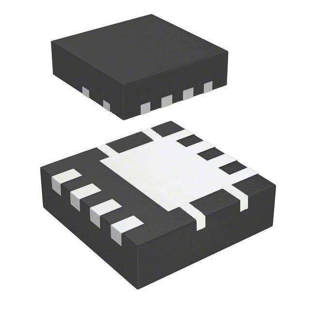
| 描述 | MOSFET N-CH 12V 4A SC70-6MOSFET 12V 4A N-CH MOSFET |
| 产品分类 | FET - 单分离式半导体 |
| FET功能 | 逻辑电平门 |
| FET类型 | MOSFET N 通道,金属氧化物 |
| Id-ContinuousDrainCurrent | 4 A |
| Id-连续漏极电流 | 4 A |
| 品牌 | Vishay / SiliconixVishay Siliconix |
| 产品手册 | |
| 产品图片 |
|
| rohs | 符合RoHS无铅 / 符合限制有害物质指令(RoHS)规范要求 |
| 产品系列 | 晶体管,MOSFET,Vishay / Siliconix SI1422DH-T1-GE3TrenchFET® |
| 数据手册 | |
| 产品型号 | SI1422DH-T1-GE3SI1422DH-T1-GE3 |
| Pd-PowerDissipation | 2.8 W |
| Pd-功率耗散 | 2.8 W |
| Qg-GateCharge | 13.1 nC |
| Qg-栅极电荷 | 13.1 nC |
| RdsOn-Drain-SourceResistance | 29 mOhms |
| RdsOn-漏源导通电阻 | 29 mOhms |
| Vds-Drain-SourceBreakdownVoltage | 12 V |
| Vds-漏源极击穿电压 | 12 V |
| Vgs-Gate-SourceBreakdownVoltage | 8 V |
| Vgs-栅源极击穿电压 | 8 V |
| Vgsth-Gate-SourceThresholdVoltage | 0.4 V |
| Vgsth-栅源极阈值电压 | 0.4 V |
| 上升时间 | 10 ns |
| 下降时间 | 10 ns |
| 不同Id时的Vgs(th)(最大值) | 1V @ 250µA |
| 不同Vds时的输入电容(Ciss) | 725pF @ 6V |
| 不同Vgs时的栅极电荷(Qg) | 20nC @ 8V |
| 不同 Id、Vgs时的 RdsOn(最大值) | 26 毫欧 @ 5.1A,4.5V |
| 产品种类 | MOSFET |
| 供应商器件封装 | SC-70-6 (SOT-363) |
| 其它名称 | SI1422DH-T1-GE3CT |
| 典型关闭延迟时间 | 20 ns |
| 功率-最大值 | 2.8W |
| 包装 | 剪切带 (CT) |
| 商标 | Vishay / Siliconix |
| 安装类型 | 表面贴装 |
| 安装风格 | SMD/SMT |
| 导通电阻 | 29 mOhms |
| 封装 | Reel |
| 封装/外壳 | 6-TSSOP,SC-88,SOT-363 |
| 封装/箱体 | SOT-363-6 |
| 工厂包装数量 | 3000 |
| 晶体管极性 | N-Channel |
| 最大工作温度 | + 150 C |
| 最小工作温度 | - 55 C |
| 标准包装 | 1 |
| 正向跨导-最小值 | 30 S |
| 汲极/源极击穿电压 | 12 V |
| 漏极连续电流 | 4 A |
| 漏源极电压(Vdss) | 12V |
| 电流-连续漏极(Id)(25°C时) | 4A (Tc) |
| 配置 | Single |
| 零件号别名 | SI1422DH-GE3 |


- 商务部:美国ITC正式对集成电路等产品启动337调查
- 曝三星4nm工艺存在良率问题 高通将骁龙8 Gen1或转产台积电
- 太阳诱电将投资9.5亿元在常州建新厂生产MLCC 预计2023年完工
- 英特尔发布欧洲新工厂建设计划 深化IDM 2.0 战略
- 台积电先进制程称霸业界 有大客户加持明年业绩稳了
- 达到5530亿美元!SIA预计今年全球半导体销售额将创下新高
- 英特尔拟将自动驾驶子公司Mobileye上市 估值或超500亿美元
- 三星加码芯片和SET,合并消费电子和移动部门,撤换高东真等 CEO
- 三星电子宣布重大人事变动 还合并消费电子和移动部门
- 海关总署:前11个月进口集成电路产品价值2.52万亿元 增长14.8%


PDF Datasheet 数据手册内容提取
New Product Si1422DH Vishay Siliconix N-Channel 12 V (D-S) MOSFET FEATURES PRODUCT SUMMARY • Halogen-free According to IEC 61249-2-21 VDS (V) RDS(on) (Ω) ID (A)a Qg (Typ.) Definition 0.026 at VGS = 4.5 V 4 (cid:129) TrenchFET® Power MOSFET 12 0.030 at VGS = 2.5 V 4 7.5 nC (cid:129) 100 % Rg Tested (cid:129) Compliant to RoHS Directive 2002/95/EC 0.036 at V = 1.8 V 4 GS APPLICATIONS (cid:129) Load Switch, PA Switch and Battery Switch for Portable Devices SOT-363 (cid:129) High Frequency dc-to-dc Converters SC-70 (6-LEADS) (cid:129) Low On-Resistance Switching D D 1 6 D Marking Code D 2 5 D AO XXY Y Lot Traceability G G 3 4 S and Date Code Part # Code Top View S Ordering Information: Si1422DH-T1-GE3 (Lead (Pb)-free and Halogen-free) N-Channel MOSFET ABSOLUTE MAXIMUM RATINGS T = 25 °C, unless otherwise noted A Parameter Symbol Limit Unit Drain-Source Voltage V 12 DS V Gate-Source Voltage V ± 8 GS T = 25 °C 4a F T = 70 °C 4a F Continuous Drain Current (T = 150 °C) I J T = 25 °C D 4b, c A T = 70 °C 4b, c A A Pulsed Drain Current I 20 DM T = 25 °C 2.3a F Continuous Source-Drain Diode Current I T = 25 °C S 1.3b, c A TF = 25 °C 2.8 TF = 70 °C 1.8 Maximum Power Dissipation P W T = 25 °C D 1.56b, c A T = 70 °C 1.0b, c A Operating Junction and Storage Temperature Range TJ, Tstg - 55 to 150 °C Soldering Recommendations (Peak Temperature) 260 THERMAL RESISTANCE RATINGS Parameter Symbol Typical Maximum Unit Maximum Junction-to-Ambientb, d t ≤ 5 s R 60 80 thJA °C/W Maximum Junction-to-Foot (Drain) Steady State R 34 45 thJF Notes: a. T = 25 °C, package limited. F b. Surface mounted on 1" x 1" FR4 board. c. t = 5 s. d. Maximum under steady state conditions is 125 °C/W. Document Number: 66701 www.vishay.com S10-1287-Rev. A, 31-May-10 1
New Product Si1422DH Vishay Siliconix SPECIFICATIONS T = 25 °C, unless otherwise noted J Parameter Symbol Test Conditions Min. Typ. Max. Unit Static Drain-Source Breakdown Voltage VDS VGS = 0 V, ID = 250 µA 12 V VDS Temperature Coefficient ΔVDS/TJ 11 ID = 250 µA mV/°C VGS(th) Temperature Coefficient ΔVGS(th)/TJ - 2.7 Gate-Source Threshold Voltage VGS(th) VDS = VGS, ID = 250 µA 0.4 1.0 V Gate-Source Leakage IGSS VDS = 0 V, VGS = ± 8 V ± 100 nA VDS = 12 V, VGS = 0 V 1 Zero Gate Voltage Drain Current IDSS µA VDS = 12 V, VGS = 0 V, TJ = 55 °C 10 On-State Drain Currenta ID(on) VDS ≥ 5 V, VGS = 4.5 V 15 A VGS = 4.5 V, ID = 5.1 A 0.021 0.026 Drain-Source On-State Resistancea RDS(on) VGS = 2.5 V, ID = 4.7 A 0.024 0.030 Ω VGS = 1.8 V, ID = 2.5 A 0.029 0.036 Forward Transconductancea gfs VDS = 10 V, ID = 5.1 A 30 S Dynamicb Input Capacitance Ciss 725 Output Capacitance Coss VDS = 6 V, VGS = 0 V, f = 1 MHz 195 pF Reverse Transfer Capacitance Crss 90 Total Gate Charge Qg VDS = 6 V, VGS = 8 V, ID = 9 A 13.1 20 7.5 12 nC Gate-Source Charge Qgs VDS = 6 V, VGS = 4.5 V, ID = 9 A 1.1 Gate-Drain Charge Qgd 0.8 Gate Resistance Rg f = 1 MHz 0.5 2.5 5 Ω Turn-On Delay Time td(on) 10 15 Rise Time tr VDD = 6 V, RL = 0.83 Ω 10 15 Turn-Off Delay Time td(off) ID ≅ 7.2 A, VGEN = 4.5 V, Rg = 1 Ω 20 30 Fall Time tf 10 15 ns Turn-On Delay Time td(on) 5 10 Rise Time tr VDD = 6 V, RL = 0.83 Ω 10 15 Turn-Off Delay Time td(off) ID ≅ 7.2 A, VGEN = 8 V, Rg = 1 Ω 20 30 Fall Time tf 10 15 Drain-Source Body Diode Characteristics Continuous Source-Drain Diode Current IS TC = 25 °C 4 A Pulse Diode Forward Current ISM 20 Body Diode Voltage VSD IS = 7.2 A, VGS = 0 V 0.8 1.2 V Body Diode Reverse Recovery Time trr 15 30 ns Body Diode Reverse Recovery Charge Qrr 4 8 nC I = 7.2 A, dI/dt = 100 A/µs, T = 25 °C F J Reverse Recovery Fall Time ta 8 ns Reverse Recovery Rise Time tb 7 Notes: a. Pulse test; pulse width ≤ 300 µs, duty cycle ≤ 2 %. b. Guaranteed by design, not subject to production testing. Stresses beyond those listed under “Absolute Maximum Ratings” may cause permanent damage to the device. These are stress ratings only, and functional operation of the device at these or any other conditions beyond those indicated in the operational sections of the specifications is not implied. Exposure to absolute maximum rating conditions for extended periods may affect device reliability. www.vishay.com Document Number: 66701 2 S10-1287-Rev. A, 31-May-10
New Product Si1422DH Vishay Siliconix TYPICAL CHARACTERISTICS 25°C, unless otherwise noted 20 10 VGS=5Vthru2V 16 8 A) A) ( ( ent 12 VGS=1.5V ent 6 Curr Curr TC=25 °C n n ai ai Dr 8 Dr 4 - - D D I I TC=125 °C 4 2 VGS=1V 0 0 TC=- 55 °C 0.0 0.5 1.0 1.5 2.0 2.5 3.0 0.0 0.3 0.6 0.9 1.2 1.5 VDS-Drain-to-SourceVoltage(V) VGS-Gate-to-SourceVoltage(V) Output Characteristics Transfer Characteristics 0.06 1000 Ciss 0.05 800 Ω) ( nce 0.04 pF) a ( sist VGS=1.8V nce 600 e a n-R 0.03 VGS=2.5V acit O p - Ca 400 S(on) 0.02 VGS=4.5V C - Coss D R 200 0.01 Crss 0 0 0 4 8 12 16 20 0 2 4 6 8 10 12 ID-DrainCurrent(A) VDS-Drain-to-SourceVoltage(V) On-Resistance vs. Drain Current Capacitance 8 1.5 ID=9A VDS=6V 1.4 ID=5.1 A VGS=2.5V,1.8V V) - Gate-to-SourceVoltage(S 246 VDS=3V VDS=9.6V R- On-ResistanceDS(on)(Normalized) 01111.....90123 VGS=4.5V G V 0.8 0 0.7 0 3 6 9 12 15 - 50 - 25 0 25 50 75 100 125 150 Qg-TotalGateCharge(nC) TJ-JunctionTemperature(°C) Gate Charge On-Resistance vs. Junction Temperature Document Number: 66701 www.vishay.com S10-1287-Rev. A, 31-May-10 3
New Product Si1422DH Vishay Siliconix TYPICAL CHARACTERISTICS 25°C, unless otherwise noted 100 0.06 ID=5.1A 0.05 Ω) nt(A) 10 ance( 0.04 TJ=125 °C Curre Resist 0.03 - Source 1 TJ=150 °C TJ=25 °C - On-on) 0.02 TJ=25 °C S S( I RD 0.01 0.1 0 0.0 0.2 0.4 0.6 0.8 1.0 1.2 0 1 2 3 4 5 VSD-Source-to-DrainVoltage(V) VGS-Gate-to-SourceVoltage(V) Soure-Drain Diode Forward Voltage On-Resistance vs. Gate-to-Source Voltage 0.8 30 0.7 25 ID=250μA 0.6 20 V) W) (GS(th) 0.5 Power ( 15 V 0.4 10 0.3 5 0.2 0 - 50 - 25 0 25 50 75 100 125 150 0.001 0.01 0.1 1 10 100 1000 TJ- Temperature(°C) Time (s) Threshold Voltage Single Pulse Power, Junction-to-Ambient 100 LimitedbyRDS(on)* 10 100μs A) ( nt urre 1ms C 1 n 10ms ai Dr - 100ms ID 0.1 TA=25 °C 1s,10s SinglePulse DC BVDSSLimited 0.01 0.1 1 10 100 VDS-Drain-to-SourceVoltage(V) *VGS>minimumVGSatwhichRDS(on)isspecified Safe Operating Area, Junction-to-Ambient www.vishay.com Document Number: 66701 4 S10-1287-Rev. A, 31-May-10
New Product Si1422DH Vishay Siliconix TYPICAL CHARACTERISTICS 25°C, unless otherwise noted 10 3.0 2.5 8 urrent(A) 6 pation (W) 2.0 C si 1.5 Drain 4 PackageLimited er Dis - ow 1.0 D P I 2 0.5 0 0.0 0 25 50 75 100 125 150 25 50 75 100 125 150 TC-CaseTemperature(°C) TF -Foot Temperature(°C) Current Derating* Power Derating * The power dissipation P is based on T = 150 °C, using junction-to-case thermal resistance, and is more useful in settling the upper D J(max) dissipation limit for cases where additional heatsinking is used. It is used to determine the current rating, when this rating falls below the package limit. Document Number: 66701 www.vishay.com S10-1287-Rev. A, 31-May-10 5
New Product Si1422DH Vishay Siliconix TYPICAL CHARACTERISTICS 25°C, unless otherwise noted 1 DutyCycle=0.5 nt e Transiance 0.2 ctivemped 0.1 Notes: edEffeermalI 0.1 0.05 PDM zh maliT t1 Nor 0.02 1.DutyCyclet,2D= t1 t2 2.PerUnitBase=RthJA=125 °C/W 3.TJM-TA=PDMZthJA(t) SinglePulse 4.SurfaceMounted 0.01 10-4 10-3 10-2 10-1 1 10 100 1000 SquareWavePulseDuration(s) Normalized Thermal Transient Impedance, Junction-to-Ambient 1 DutyCycle=0.5 nt e Transiance 0.2 ctivemped 0.1 EffemalI 0.1 0.05 eder zh aliT 0.02 m or N SinglePulse 0.01 10-4 10-3 10-2 10-1 1 10 SquareWavePulseDuration(s) Normalized Thermal Transient Impedance, Junction-to-Foot Vishay Siliconix maintains worldwide manufacturing capability. Products may be manufactured at one of several qualified locations. Reliability data for Silicon Technology and Package Reliability represent a composite of all qualified locations. For related documents such as package/tape drawings, part marking, and reliability data, see www.vishay.com/ppg?66701. www.vishay.com Document Number: 66701 6 S10-1287-Rev. A, 31-May-10
Package Information Vishay Siliconix (cid:1)(cid:2)(cid:3)(cid:4)(cid:5)(cid:6)(cid:7)(cid:7)(cid:7)(cid:8)(cid:3)(cid:9)(cid:10)(cid:11)(cid:12)(cid:1) (cid:13)(cid:14)(cid:9)(cid:9)(cid:14)(cid:13)(cid:10)(cid:15)(cid:10)(cid:16)(cid:1) (cid:14)(cid:17)(cid:2)(cid:18)(cid:10)(cid:1) Dim Min Nom Max Min Nom Max 6 5 4 A 0.90 – 1.10 0.035 – 0.043 E1 E A1 – – 0.10 – – 0.004 1 2 3 A2 0.80 – 1.00 0.031 – 0.039 b 0.15 – 0.30 0.006 – 0.012 -B- c 0.10 – 0.25 0.004 – 0.010 e b D 1.80 2.00 2.20 0.071 0.079 0.087 e1 E 1.80 2.10 2.40 0.071 0.083 0.094 D -A- E1 1.15 1.25 1.35 0.045 0.049 0.053 c e 0.65BSC 0.026BSC A2 A e1 1.20 1.30 1.40 0.047 0.051 0.055 L 0.10 0.20 0.30 0.004 0.008 0.012 L 7(cid:1)Nom 7(cid:1)Nom A1 ECN: S-03946—Rev. B, 09-Jul-01 DWG: 5550 Document Number: 71154 www.vishay.com 06-Jul-01 1
AN815 Vishay Siliconix (cid:1) Single-Channel LITTLE FOOT SC-70 6-Pin MOSFET Copper Leadframe Version Recommended Pad Pattern and Thermal Performance INTRODUCTION EVALUATION BOARDS (cid:1) SINGLE SC70-6 The new single 6-pin SC-70 package with a copper leadframe enables improved on-resistance values and enhanced The evaluation board (EVB) measures 0.6 inches by thermal performance as compared to the existing 3-pin and 0.5 inches. The copper pad traces are the same as in Figure 2. 6-pin packages with Alloy 42 leadframes. These devices are The board allows examination from the outer pins to 6-pin DIP intended for small to medium load applications where a connections, permitting test sockets to be used in evaluation miniaturized package is required. Devices in this package testing. See Figure 3. come in a range of on-resistance values, in n-channel and p-channel versions. This technical note discusses pin-outs, package outlines, pad patterns, evaluation board layout, and thermal performance for the single-channel version. 52 (mil) BASIC PAD PATTERNS 6 5 4 See Application Note 826, Recommended Minimum Pad Patterns With Outline Drawing Access for Vishay Siliconix 96 (mil) MOSFETs, (http://www.vishay.com/doc?72286) for the basic 71 (mil) pad layout and dimensions. These pad patterns are sufficient for the low to medium power applications for which this package is intended. Increasing the drain pad pattern yields a 1 2 3 26 (mil) reduction in thermal resistance and is a preferred footprint. 13 (mil) The availability of four drain leads rather than the traditional single drain lead allows a better thermal path from the package 0, 0 (mil) to the PCB and external environment. 18 (mil) 26 (mil) PIN-OUT 16 (mil) Figure 1 shows the pin-out description and Pin 1 FIGURE 2. SC-70 (6 leads) Single identification.The pin-out of this device allows the use of four pins as drain leads, which helps to reduce on-resistance and junction-to-ambient thermal resistance. SOT-363 SC-70 (6-LEADS) The thermal performance of the single 6-pin SC-70 has been measured on the EVB, comparing both the copper and D 1 6 D Alloy 42 leadframes. This test was first conducted on the traditional Alloy 42 leadframe and was then repeated using the D 2 5 D 1-inch2 PCB with dual-side copper coating. G 3 4 S Top View FIGURE 1. For package dimensions see outline drawing SC-70 (6-Leads) (http://www.vishay.com/doc?71154) Document Number: 71334 www.vishay.com 12-Dec-03 1
AN815 Vishay Siliconix Front of Board SC70-6 Back of Board SC70-6 vishay.com FIGURE 3. THERMAL PERFORMANCE Junction-to-Foot Thermal Resistance COOPER LEADFRAME (Package Performance) Room Ambient 25 (cid:1)C Elevated Ambient 60 (cid:1)C The junction to foot thermal resistance is a useful method of T (cid:2)T T (cid:2)T comparing different packages thermal performance. PD(cid:1) J(mRax(cid:1)) A PD(cid:1) J(mRax(cid:1)) A JA JA A helpful way of presenting the thermal performance of the PD(cid:1) 15012oC4o(cid:2)C(cid:3)2W5oC PD(cid:1) 15012oC4o(cid:2)C(cid:3)6W0oC 6tr-aPdiinti oSnCa-l 7A0l locoy p4p2e rv elerasidofnra.me device is to compare it to the PD(cid:1) 1.01W PD(cid:1) 726mW As can be seen from the calculations above, the compact 6-pin SC-70 copper leadframe LITTLE FOOT power MOSFET can Thermal performance for the 6-pin SC-70 measured as handle up to 1 W under the stated conditions. junction-to-foot thermal resistance, where the “foot” is the drain lead of the device at the bottom where it meets the PCB. The junction-to-foot thermal resistance is typically 40(cid:2)C/W in Testing the copper leadframe and 163(cid:2)C/W in the Alloy 42 leadframe To further aid comparison of copper and Alloy 42 leadframes, — a four-fold improvement. This improved performance is Figure 5 illustrates single-channel 6-pin SC-70 thermal obtained by the enhanced thermal conductivity of copper over performance on two different board sizes and two different pad Alloy 42. patterns. The measured steady-state values of R(cid:1)JA for the two leadframes are as follows: LITTLE FOOT 6-PIN SC-70 Power Dissipation Alloy 42 Copper The typical R(cid:1)JA for the single 6-pin SC-70 with copper leadframe is 103(cid:2)C/W steady-state, compared with 212(cid:2)C/W 1) Minimum recommended pad pattern on 329.7(cid:2)C/W 208.5(cid:2)C/W the EVB board V (see Figure 3. for the Alloy 42 version. The figures are based on the 1-inch2 FR4 test board. The following example shows how the thermal 2m)a Ixnidmuusmtry c sotpapnedra brdo t1h- isnicdhe2s .PCB with 211.8(cid:2)C/W 103.5(cid:2)C/W resistance impacts power dissipation for the two different The results indicate that designers can reduce thermal leadframes at varying ambient temperatures. resistance (R(cid:1) ) by 36% simply by using the copper JA ALLOY 42 LEADFRAME leadframe device rather than the Alloy 42 version. In this example, a 121(cid:2)C/W reduction was achieved without an Room Ambient 25 (cid:1)C Elevated Ambient 60 (cid:1)C increase in board area. If increasing in board size is feasible, a further 105(cid:2)C/W reduction could be obtained by utilizing a PD(cid:1) TJ(mRax(cid:1))(cid:2)TA PD(cid:1) TJ(mRax(cid:1))(cid:2)TA 1-inch2 square PCB area. JA JA The copper leadframe versions have the following suffix: PD(cid:1) 15021oC2o(cid:2)C(cid:3)2W5oC PD(cid:1) 15021oC2o(cid:2)C(cid:3)2W5oC Single: Si14xxEDH PD(cid:1) 590mW PD(cid:1) 425mW DCuoaml:plementary: SSii1159xxxxEEDDHH www.vishay.com Document Number: 71334 2 12-Dec-03
AN815 Vishay Siliconix 400 250 320 200 W) W) C/ C/ e ( 240 e ( 150 c c an Alloy an st 42 st Alloy esi esi 42 R 160 R 100 al al m m her Copper her T T 80 50 Copper 0 0 10-5 10-4 10-3 10-2 10-1 1 10 100 1000 10-5 10-4 10-3 10-2 10-1 1 10 100 1000 Time (Secs) Time (Secs) FIGURE 4. Leadframe Comparison on EVB FIGURE 5. Leadframe Comparison on Alloy 42 1-inch2 PCB Document Number: 71334 www.vishay.com 12-Dec-03 3
Application Note 826 Vishay Siliconix RECOMMENDED MINIMUM PADS FOR SC-70: 6-Lead 0.067 (1.702) 6 8) 2 4 0 6 0. 0. ( 0.096 (2.438) 0.045 (1.143) 0.016 0.026 0.010 (0.406) (0.648) (0.241) Recommended Minimum Pads Dimensions in Inches/(mm) Return to Index Return to Index E T O N N O I T A C I L P P A www.vishay.com Document Number: 72602 18 Revision: 21-Jan-08
Legal Disclaimer Notice www.vishay.com Vishay Disclaimer ALL PRODUCT, PRODUCT SPECIFICATIONS AND DATA ARE SUBJECT TO CHANGE WITHOUT NOTICE TO IMPROVE RELIABILITY, FUNCTION OR DESIGN OR OTHERWISE. Vishay Intertechnology, Inc., its affiliates, agents, and employees, and all persons acting on its or their behalf (collectively, “Vishay”), disclaim any and all liability for any errors, inaccuracies or incompleteness contained in any datasheet or in any other disclosure relating to any product. Vishay makes no warranty, representation or guarantee regarding the suitability of the products for any particular purpose or the continuing production of any product. To the maximum extent permitted by applicable law, Vishay disclaims (i) any and all liability arising out of the application or use of any product, (ii) any and all liability, including without limitation special, consequential or incidental damages, and (iii) any and all implied warranties, including warranties of fitness for particular purpose, non-infringement and merchantability. Statements regarding the suitability of products for certain types of applications are based on Vishay’s knowledge of typical requirements that are often placed on Vishay products in generic applications. Such statements are not binding statements about the suitability of products for a particular application. It is the customer’s responsibility to validate that a particular product with the properties described in the product specification is suitable for use in a particular application. Parameters provided in datasheets and / or specifications may vary in different applications and performance may vary over time. All operating parameters, including typical parameters, must be validated for each customer application by the customer’s technical experts. Product specifications do not expand or otherwise modify Vishay’s terms and conditions of purchase, including but not limited to the warranty expressed therein. Except as expressly indicated in writing, Vishay products are not designed for use in medical, life-saving, or life-sustaining applications or for any other application in which the failure of the Vishay product could result in personal injury or death. Customers using or selling Vishay products not expressly indicated for use in such applications do so at their own risk. Please contact authorized Vishay personnel to obtain written terms and conditions regarding products designed for such applications. No license, express or implied, by estoppel or otherwise, to any intellectual property rights is granted by this document or by any conduct of Vishay. Product names and markings noted herein may be trademarks of their respective owners. © 2017 VISHAY INTERTECHNOLOGY, INC. ALL RIGHTS RESERVED Revision: 08-Feb-17 1 Document Number: 91000