ICGOO在线商城 > 分立半导体产品 > 晶体管 - FET,MOSFET - 单 > 2SK1828TE85LF
 Datasheet下载
- 型号: 2SK1828TE85LF
- 制造商: Toshiba America Electronic Components, Inc.
- 库位|库存: xxxx|xxxx
- 要求:
| 数量阶梯 | 香港交货 | 国内含税 |
| +xxxx | $xxxx | ¥xxxx |
查看当月历史价格
查看今年历史价格
2SK1828TE85LF产品简介:
ICGOO电子元器件商城为您提供2SK1828TE85LF由Toshiba America Electronic Components, Inc.设计生产,在icgoo商城现货销售,并且可以通过原厂、代理商等渠道进行代购。 2SK1828TE85LF价格参考。Toshiba America Electronic Components, Inc.2SK1828TE85LF封装/规格:晶体管 - FET,MOSFET - 单, 表面贴装 N 沟道 20V 50mA(Ta) 200mW(Ta) SC-59。您可以下载2SK1828TE85LF参考资料、Datasheet数据手册功能说明书,资料中有2SK1828TE85LF 详细功能的应用电路图电压和使用方法及教程。
型号为2SK1828TE85LF的晶体管属于Toshiba Semiconductor and Storage(东芝半导体与存储)旗下产品,是一款N沟道增强型MOSFET。该器件常用于需要高效开关和功率控制的电子电路中。

其主要应用场景包括:

1. 电源管理:适用于DC-DC转换器、电源开关等电路,用于提高电源转换效率并减小体积。
2. 电机驱动:在小型电机控制电路中作为开关元件,实现对电机启停和转速的控制。
3. 负载开关:用于控制电池供电设备中的负载通断,延长电池寿命。
4. LED照明:在LED驱动电路中作为调光或开关元件使用。
5. 消费类电子产品:如笔记本电脑、平板电脑、智能家电等设备中的功率控制模块。

该MOSFET具有低导通电阻、封装小巧、响应速度快等优点,适合高频开关应用。由于其为表面贴装型封装(如SOP或类似封装形式),也适用于自动化生产和高密度电路设计。
| 参数 | 数值 |
| 产品目录 | |
| 描述 | MOSFET N-CH 20V 50MA S-MINI |
| 产品分类 | FET - 单 |
| FET功能 | 逻辑电平栅极,2.5V 驱动 |
| FET类型 | MOSFET N 通道,金属氧化物 |
| 品牌 | Toshiba Semiconductor and Storage |
| 数据手册 | |
| 产品图片 |
|
| 产品型号 | 2SK1828TE85LF |
| rohs | 无铅 / 符合限制有害物质指令(RoHS)规范要求 |
| 产品系列 | - |
| 不同Id时的Vgs(th)(最大值) | 1.5V @ 100µA |
| 不同Vds时的输入电容(Ciss) | 5.5pF @ 3V |
| 不同Vgs时的栅极电荷(Qg) | - |
| 不同 Id、Vgs时的 RdsOn(最大值) | 40欧姆 @ 10mA, 2.5V |
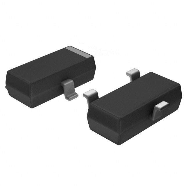
| 供应商器件封装 | SC-59 |
| 其它名称 | 2SK1828TE85LFDKR |
| 功率-最大值 | 200mW |
| 包装 | Digi-Reel® |
| 安装类型 | 表面贴装 |
| 封装/外壳 | TO-236-3,SC-59,SOT-23-3 |
| 标准包装 | 1 |
| 漏源极电压(Vdss) | 20V |
| 电流-连续漏极(Id)(25°C时) | 50mA(Ta) |


PDF Datasheet 数据手册内容提取
2SK1828 TOSHIBA Field Effect Transistor Silicon N Channel MOS Type 2SK1828 High Speed Switching Applications Unit: mm Analog Switch Applications • 2.5 V gate drive • Low threshold voltage: Vth = 0.5 to 1.5 V • High speed • Enhancement-mode • Small package Marking Equivalent Circuit JEDEC TO-236MOD JEITA SC-59 TOSHIBA 2-3F1F Weight: 0.012 g (typ.) Absolute Maximum Ratings (Ta = 25°C) Characteristics Symbol Rating Unit Drain-source voltage VDS 20 V Gate-source voltage VGSS 10 V DC drain current ID 50 mA Drain power dissipation PD 200 mW Channel temperature Tch 150 °C Storage temperature range Tstg −55 to 150 °C Note: Using continuously under heavy loads (e.g. the application of high temperature/current/voltage and the significant change in temperature, etc.) may cause this product to decrease in the reliability significantly even if the operating conditions (i.e. operating temperature/current/voltage, etc.) are within the absolute maximum ratings. Please design the appropriate reliability upon reviewing the Toshiba Semiconductor Reliability Handbook (“Handling Precautions”/“Derating Concept and Methods”) and individual reliability data (i.e. reliability test report and estimated failure rate, etc). Note: This transistor is electrostatic sensitive device. Please handle with caution. Start of commercial production 1991-02 1 2014-03-01
2SK1828 Electrical Characteristics (Ta = 25°C) Characteristics Symbol Test Condition Min Typ. Max Unit Gate leakage current IGSS VGS = 10 V, VDS = 0 ⎯ ⎯ 1 μA Drain-source breakdown voltage V (BR) DSS ID = 100 μA, VGS = 0 20 ⎯ ⎯ V Drain cut-off current IDSS VDS = 20 V, VGS = 0 ⎯ ⎯ 1 μA Gate threshold voltage Vth VDS = 3 V, ID = 0.1 mA 0.5 ⎯ 1.5 V Forward transfer admittance ⎪Yfs⎪ VDS = 3 V, ID = 10 mA 20 ⎯ ⎯ mS Drain-source ON resistance RDS (ON) ID = 10 mA, VGS = 2.5 V ⎯ 20 40 Ω Input capacitance Ciss VDS = 3 V, VGS = 0, f = 1 MHz ⎯ 5.5 ⎯ pF Reverse transfer capacitance Crss VDS = 3 V, VGS = 0, f = 1 MHz ⎯ 1.6 ⎯ pF Output capacitance Coss VDS = 3 V, VGS = 0, f = 1 MHz ⎯ 6.5 ⎯ pF Turn-on time ton VDD = 3 V, ID = 10 mA, VGS = 0 to 2.5 V ⎯ 0.14 ⎯ Switching time μs Turn-off time toff VDD = 3 V, ID = 10 mA, VGS = 0 to 2.5 V ⎯ 0.14 ⎯ Switching Time Test Circuit 2 2014-03-01
2SK1828 3 2014-03-01
2SK1828 4 2014-03-01
2SK1828 RESTRICTIONS ON PRODUCT USE • Toshiba Corporation, and its subsidiaries and affiliates (collectively "TOSHIBA"), reserve the right to make changes to the information in this document, and related hardware, software and systems (collectively "Product") without notice. • This document and any information herein may not be reproduced without prior written permission from TOSHIBA. Even with TOSHIBA's written permission, reproduction is permissible only if reproduction is without alteration/omission. • Though TOSHIBA works continually to improve Product's quality and reliability, Product can malfunction or fail. Customers are responsible for complying with safety standards and for providing adequate designs and safeguards for their hardware, software and systems which minimize risk and avoid situations in which a malfunction or failure of Product could cause loss of human life, bodily injury or damage to property, including data loss or corruption. Before customers use the Product, create designs including the Product, or incorporate the Product into their own applications, customers must also refer to and comply with (a) the latest versions of all relevant TOSHIBA information, including without limitation, this document, the specifications, the data sheets and application notes for Product and the precautions and conditions set forth in the "TOSHIBA Semiconductor Reliability Handbook" and (b) the instructions for the application with which the Product will be used with or for. Customers are solely responsible for all aspects of their own product design or applications, including but not limited to (a) determining the appropriateness of the use of this Product in such design or applications; (b) evaluating and determining the applicability of any information contained in this document, or in charts, diagrams, programs, algorithms, sample application circuits, or any other referenced documents; and (c) validating all operating parameters for such designs and applications. TOSHIBA ASSUMES NO LIABILITY FOR CUSTOMERS' PRODUCT DESIGN OR APPLICATIONS. • PRODUCT IS NEITHER INTENDED NOR WARRANTED FOR USE IN EQUIPMENTS OR SYSTEMS THAT REQUIRE EXTRAORDINARILY HIGH LEVELS OF QUALITY AND/OR RELIABILITY, AND/OR A MALFUNCTION OR FAILURE OF WHICH MAY CAUSE LOSS OF HUMAN LIFE, BODILY INJURY, SERIOUS PROPERTY DAMAGE AND/OR SERIOUS PUBLIC IMPACT ("UNINTENDED USE"). Except for specific applications as expressly stated in this document, Unintended Use includes, without limitation, equipment used in nuclear facilities, equipment used in the aerospace industry, medical equipment, equipment used for automobiles, trains, ships and other transportation, traffic signaling equipment, equipment used to control combustions or explosions, safety devices, elevators and escalators, devices related to electric power, and equipment used in finance-related fields. IF YOU USE PRODUCT FOR UNINTENDED USE, TOSHIBA ASSUMES NO LIABILITY FOR PRODUCT. For details, please contact your TOSHIBA sales representative. • Do not disassemble, analyze, reverse-engineer, alter, modify, translate or copy Product, whether in whole or in part. • Product shall not be used for or incorporated into any products or systems whose manufacture, use, or sale is prohibited under any applicable laws or regulations. • The information contained herein is presented only as guidance for Product use. No responsibility is assumed by TOSHIBA for any infringement of patents or any other intellectual property rights of third parties that may result from the use of Product. No license to any intellectual property right is granted by this document, whether express or implied, by estoppel or otherwise. • ABSENT A WRITTEN SIGNED AGREEMENT, EXCEPT AS PROVIDED IN THE RELEVANT TERMS AND CONDITIONS OF SALE FOR PRODUCT, AND TO THE MAXIMUM EXTENT ALLOWABLE BY LAW, TOSHIBA (1) ASSUMES NO LIABILITY WHATSOEVER, INCLUDING WITHOUT LIMITATION, INDIRECT, CONSEQUENTIAL, SPECIAL, OR INCIDENTAL DAMAGES OR LOSS, INCLUDING WITHOUT LIMITATION, LOSS OF PROFITS, LOSS OF OPPORTUNITIES, BUSINESS INTERRUPTION AND LOSS OF DATA, AND (2) DISCLAIMS ANY AND ALL EXPRESS OR IMPLIED WARRANTIES AND CONDITIONS RELATED TO SALE, USE OF PRODUCT, OR INFORMATION, INCLUDING WARRANTIES OR CONDITIONS OF MERCHANTABILITY, FITNESS FOR A PARTICULAR PURPOSE, ACCURACY OF INFORMATION, OR NONINFRINGEMENT. • Do not use or otherwise make available Product or related software or technology for any military purposes, including without limitation, for the design, development, use, stockpiling or manufacturing of nuclear, chemical, or biological weapons or missile technology products (mass destruction weapons). Product and related software and technology may be controlled under the applicable export laws and regulations including, without limitation, the Japanese Foreign Exchange and Foreign Trade Law and the U.S. Export Administration Regulations. Export and re-export of Product or related software or technology are strictly prohibited except in compliance with all applicable export laws and regulations. • Please contact your TOSHIBA sales representative for details as to environmental matters such as the RoHS compatibility of Product. Please use Product in compliance with all applicable laws and regulations that regulate the inclusion or use of controlled substances, including without limitation, the EU RoHS Directive. TOSHIBA ASSUMES NO LIABILITY FOR DAMAGES OR LOSSES OCCURRING AS A RESULT OF NONCOMPLIANCE WITH APPLICABLE LAWS AND REGULATIONS. 5 2014-03-01