ICGOO在线商城 > 分立半导体产品 > 晶体管 - FET,MOSFET - 单 > FDB8445
 Datasheet下载
- 型号: FDB8445
- 制造商: Fairchild Semiconductor
- 库位|库存: xxxx|xxxx
- 要求:
| 数量阶梯 | 香港交货 | 国内含税 |
| +xxxx | $xxxx | ¥xxxx |
查看当月历史价格
查看今年历史价格
FDB8445产品简介:
ICGOO电子元器件商城为您提供FDB8445由Fairchild Semiconductor设计生产,在icgoo商城现货销售,并且可以通过原厂、代理商等渠道进行代购。 FDB8445价格参考¥11.35-¥11.35。Fairchild SemiconductorFDB8445封装/规格:晶体管 - FET,MOSFET - 单, N-Channel 40V 70A (Tc) 92W (Tc) Surface Mount TO-263AB。您可以下载FDB8445参考资料、Datasheet数据手册功能说明书,资料中有FDB8445 详细功能的应用电路图电压和使用方法及教程。
FDB8445是安森美(ON Semiconductor)推出的一款高性能N沟道功率MOSFET,广泛应用于需要高效率和高开关速度的电源管理场景。其主要应用场景包括:

1. 电源转换系统:常用于开关电源(SMPS)、DC-DC转换器中,特别是在降压(Buck)和升压(Boost)拓扑结构中表现优异,适用于服务器、通信设备和工业电源模块。

2. 电机驱动:在电动工具、家用电器和工业控制中的电机驱动电路中,FDB8445凭借低导通电阻(RDS(on))和高电流处理能力,可有效降低功耗,提升驱动效率。

3. 电池管理系统(BMS):适用于便携式设备和电动交通工具中的电池保护与充放电控制,提供快速响应和可靠保护。

4. 热插拔与负载开关:因其具备良好的瞬态响应和过流保护特性,适合用于服务器背板、网络设备中的热插拔控制器。

5. 照明电源:在LED驱动电源中用于高效能量转换,支持高亮度LED照明系统的稳定运行。

FDB8445采用先进的封装技术,具有优良的散热性能和可靠性,适合在紧凑空间内实现高功率密度设计。其优化的栅极电荷和低导通损耗使其在高频工作条件下仍保持高效率,满足现代电子设备对节能和小型化的需求。
| 参数 | 数值 |
| 产品目录 | |
| ChannelMode | Enhancement |
| 描述 | MOSFET N-CH 40V 70A D2PAKMOSFET 40V N-Channel PwrTrch MOSFET |
| 产品分类 | FET - 单分离式半导体 |
| FET功能 | 逻辑电平门 |
| FET类型 | MOSFET N 通道,金属氧化物 |
| Id-ContinuousDrainCurrent | 70 A |
| Id-连续漏极电流 | 70 A |
| 品牌 | Fairchild Semiconductor |
| 产品手册 | |
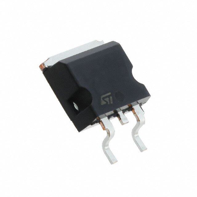
| 产品图片 |
|
| rohs | RoHS 合规性豁免无铅 / 符合限制有害物质指令(RoHS)规范要求 |
| 产品系列 | 晶体管,MOSFET,Fairchild Semiconductor FDB8445PowerTrench® |
| 数据手册 | |
| 产品型号 | FDB8445 |
| PCN封装 | |
| Pd-PowerDissipation | 92 W |
| Pd-功率耗散 | 92 W |
| RdsOn-Drain-SourceResistance | 6.8 mOhms |
| RdsOn-漏源导通电阻 | 6.8 mOhms |
| Vds-Drain-SourceBreakdownVoltage | 40 V |
| Vds-漏源极击穿电压 | 40 V |
| Vgs-Gate-SourceBreakdownVoltage | +/- 20 V |
| Vgs-栅源极击穿电压 | 20 V |
| 上升时间 | 19 ns |
| 下降时间 | 16 ns |
| 不同Id时的Vgs(th)(最大值) | 4V @ 250µA |
| 不同Vds时的输入电容(Ciss) | 3805pF @ 25V |
| 不同Vgs时的栅极电荷(Qg) | 62nC @ 10V |
| 不同 Id、Vgs时的 RdsOn(最大值) | 9 毫欧 @ 70A,10V |
| 产品目录页面 | |
| 产品种类 | MOSFET |
| 供应商器件封装 | D²PAK |
| 其它名称 | FDB8445DKR |
| 典型关闭延迟时间 | 36 ns |
| 功率-最大值 | 92W |
| 包装 | Digi-Reel® |
| 单位重量 | 1.312 g |
| 商标 | Fairchild Semiconductor |
| 安装类型 | 表面贴装 |
| 安装风格 | SMD/SMT |
| 封装 | Reel |
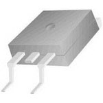
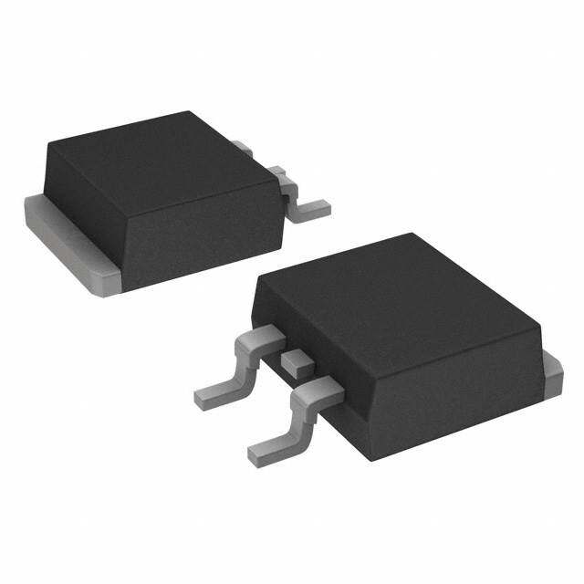
| 封装/外壳 | TO-263-3,D²Pak(2 引线+接片),TO-263AB |
| 封装/箱体 | D2PAK-2 |
| 工厂包装数量 | 800 |
| 晶体管极性 | N-Channel |
| 最大工作温度 | + 175 C |
| 最小工作温度 | - 55 C |
| 标准包装 | 1 |
| 漏源极电压(Vdss) | 40V |
| 电流-连续漏极(Id)(25°C时) | 70A (Tc) |
| 系列 | FDB8445 |
| 通道模式 | Enhancement |
| 配置 | Single |


- 商务部:美国ITC正式对集成电路等产品启动337调查
- 曝三星4nm工艺存在良率问题 高通将骁龙8 Gen1或转产台积电
- 太阳诱电将投资9.5亿元在常州建新厂生产MLCC 预计2023年完工
- 英特尔发布欧洲新工厂建设计划 深化IDM 2.0 战略
- 台积电先进制程称霸业界 有大客户加持明年业绩稳了
- 达到5530亿美元!SIA预计今年全球半导体销售额将创下新高
- 英特尔拟将自动驾驶子公司Mobileye上市 估值或超500亿美元
- 三星加码芯片和SET,合并消费电子和移动部门,撤换高东真等 CEO
- 三星电子宣布重大人事变动 还合并消费电子和移动部门
- 海关总署:前11个月进口集成电路产品价值2.52万亿元 增长14.8%


PDF Datasheet 数据手册内容提取
Is Now Part of To learn more about ON Semiconductor, please visit our website at www.onsemi.com Please note: As part of the Fairchild Semiconductor integration, some of the Fairchild orderable part numbers will need to change in order to meet ON Semiconductor’s system requirements. Since the ON Semiconductor product management systems do not have the ability to manage part nomenclature that utilizes an underscore (_), the underscore (_) in the Fairchild part numbers will be changed to a dash (-). This document may contain device numbers with an underscore (_). Please check the ON Semiconductor website to verify the updated device numbers. The most current and up-to-date ordering information can be found at www.onsemi.com. Please email any questions regarding the system integration to Fairchild_questions@onsemi.com. ON Semiconductor and the ON Semiconductor logo are trademarks of Semiconductor Components Industries, LLC dba ON Semiconductor or its subsidiaries in the United States and/or other countries. ON Semiconductor owns the rights to a number of patents, trademarks, copyrights, trade secrets, and other intellectual property. A listing of ON Semiconductor’s product/patent coverage may be accessed at www.onsemi.com/site/pdf/Patent-Marking.pdf. ON Semiconductor reserves the right to make changes without further notice to any products herein. ON Semiconductor makes no warranty, representation or guarantee regarding the suitability of its products for any particular purpose, nor does ON Semiconductor assume any liability arising out of the application or use of any product or circuit, and specifically disclaims any and all liability, including without limitation special, consequential or incidental damages. Buyer is responsible for its products and applications using ON Semiconductor products, including compliance with all laws, regulations and safety requirements or standards, regardless of any support or applications information provided by ON Semiconductor. “Typical” parameters which may be provided in ON Semiconductor data sheets and/or specifications can and do vary in different applications and actual performance may vary over time. All operating parameters, including “Typicals” must be validated for each customer application by customer’s technical experts. ON Semiconductor does not convey any license under its patent rights nor the rights of others. ON Semiconductor products are not designed, intended, or authorized for use as a critical component in life support systems or any FDA Class 3 medical devices or medical devices with a same or similar classification in a foreign jurisdiction or any devices intended for implantation in the human body. Should Buyer purchase or use ON Semiconductor products for any such unintended or unauthorized application, Buyer shall indemnify and hold ON Semiconductor and its officers, employees, subsidiaries, affiliates, and distributors harmless against all claims, costs, damages, and expenses, and reasonable attorney fees arising out of, directly or indirectly, any claim of personal injury or death associated with such unintended or unauthorized use, even if such claim alleges that ON Semiconductor was negligent regarding the design or manufacture of the part. ON Semiconductor is an Equal Opportunity/Affirmative Action Employer. This literature is subject to all applicable copyright laws and is not for resale in any manner.
F D January 2006 B 8 4 4 5 N - FDB8445 C h a n ® N-Channel PowerTrench MOSFET n e l 40V, 70A, 9mΩ P o w Features Applications e r T (cid:132) Typ rDS(on) = 6.8mΩ at VGS = 10V, ID = 70A (cid:132) Automotive Engine Control re n (cid:132) Typ Qg(10) = 44nC at VGS = 10V (cid:132) Powertrain Management c h (cid:132) Low Miller Charge (cid:132) Solenoid and Motor Drivers ® M (cid:132) Low Q Body Diode (cid:132) Electronic Transmission O rr S (cid:132) UIS Capability (Single Pulse/ Repetitive Pulse) (cid:132) Distributed Power Architecture and VRMs F E (cid:132) Qualified to AEC Q101 (cid:132) Primary Switch for 12V Systems T (cid:132) RoHS Compliant LEA D FREEIMPL EM E N T A NOIT D GATE G SOURCE DRAIN TO-263AB (FLANGE) FDB SERIES S ©2006 Fairchild Semiconductor Corporation 1 www.fairchildsemi.com FDB8445 Rev A1 (W)
F Absolute Maximum Ratings TC = 25°C unless otherwise noted D B Symbol Parameter Ratings Units 8 4 VDSS Drain to Source Voltage 40 V 4 V Gate to Source Voltage ±20 V 5 GS N Drain Current Continuous (V = 10V) (Note 1) 70 A ID Pulsed GS Figure 4 -C h E Single Pulse Avalanche Energy (Note 2) 102 mJ a AS n Power Dissipation 92 W n P D Derate above 25oC 0.6 W/oC e l T , T Operating and Storage Temperature -55 to +175 oC P J STG o w Thermal Characteristics e r T RθJC Thermal Resistance, Junction to Case 1.63 oC/W r e RθJA Tarheearmal Resistance, Junction to Ambient TO-263, 1in2 copper pad 43 oC/W nc h ® Package Marking and Ordering Information M O Device Marking Device Package Reel Size Tape Width Quantity S FDB8445 FDB8445 TO-263AB 330mm 24mm 800 units F E T Electrical Characteristics T = 25°C unless otherwise noted J Symbol Parameter Test Conditions Min Typ Max Units Off Characteristics B Drain to Source Breakdown Voltage I = 250µA, V = 0V 40 - - V VDSS D GS V = 32V - - 1 µA I Zero Gate Voltage Drain Current DS DSS VGS = 0V TJ =150°C - - 250 µA I Gate to Source Leakage Current V = ±20V - - ±100 nA GSS GS On Characteristics V Gate to Source Threshold Voltage V = V , I = 250µA 2 2.5 4 V GS(th) DS GS D I = 70A, V = 10V - 6.8 9 D GS rDS(on) Drain to Source On Resistance ID = 70A, VGS = 10V, - 13 17.2 mΩ T = 175°C J Dynamic Characteristics C Input Capacitance - 2860 3805 pF iss V = 25V, V = 0V, C Output Capacitance DS GS - 295 395 pF oss f = 1MHz C Reverse Transfer Capacitance - 180 270 pF rss R Gate Resistance f = 1MHz - 1.95 - W G Q Total Gate Charge at 10V V = 0 to 10V - 44 62 nC g(TOT) GS Qg(TH) Threshold Gate Charge VGS = 0 to 2V VDS= 20V, - 2.9 4.1 nC Q Gate to Source Gate Charge I = 70A, - 11 - nC gs D Q Gate Charge Threshold to Plateau - 8.2 - nC gs2 Q Gate to Drain Charge - 11 - nC gd 2 www.fairchildsemi.com FDB8445 Rev A1 (W)
F Electrical Characteristics T = 25°C unless otherwise noted D J B Symbol Parameter Test Conditions Min Typ Max Units 8 4 4 Switching Characteristics 5 t Turn-On Time - - 45 ns N (on) - t Turn-On Delay Time - 10 - ns C d(on) h tr Turn-On Rise Time VDD = 20V, ID = 70A - 19 - ns a td(off) Turn-Off Delay Time VGS = 10V, RGS = 5Ω - 36 - ns nn tf Turn-Off Fall Time - 16 - ns e l toff Turn-Off Time - - 81 ns P o Drain-Source Diode Characteristics w e I = 70A - - 1.25 V r V Source to Drain Diode Voltage SD T SD I = 35A - - 1.0 V r SD e t Reverse Recovery Time I = 70A, di/dt = 100A/µs - - 59 ns n rr F c Qrr Reverse Recovery Charge IF = 70A, di/dt = 100A/µs - - 77 nC h ® Notes: 1: Maximum wire current carrying capacity is 70A. M 2: Starting TJ = 25oC, L = 65µH, IAS = 56A. O S F E T This product has been designed to meet the extreme test conditions and environment demanded by the automotive industry. For a copy of the requirements, see AEC Q101 at: http://www.aecouncil.com/ All Fairchild Semiconductor products are manufactured, assembled and tested under ISO9000 and QS9000 quality systems certification. 3 www.fairchildsemi.com FDB8445 Rev A1 (W)
F D Typical Characteristics B 8 4 4 5 1.2 100 LIPLIER1.0 A) 80 CBYU RWRIERNET LIMITED VGS = 10V N-Ch MU0.8 NT ( an ON RE 60 n SIPATI0.6 N CUR 40 el Po DIS0.4 RAI w WER 0.2 I, DD 20 erT O r P e 0.0 0 n 0 25 50 75 100 125 150 175 25 50 75 100 125 150 175 c h TC, CASE TEMPERATURE(oC) TC, CASE TEMPERATURE(oC) ® M Figure 1. Normalized Power Dissipation vs Case Figure 2. Maximum Continuous Drain Current vs O Temperature Case Temperature S F 2 E DUTY CYCLE - DESCENDING ORDER T 1 L D = 0.50 A 0.20 ERMZJCθ 00..1005 D THNCE, 00..0021 PDM ALIZEPEDA0.1 t1 MM t2 RI O NOTES: N DUTY FACTOR: D = t1/t2 SINGLE PULSE PEAK TJ = PDM x ZθJC x RθJC + TC 0.01 10-5 10-4 10-3 10-2 10-1 100 101 t, RECTANGULAR PULSE DURATION(s) Figure 3. Normalized Maximum Transient Thermal Impedance 2000 TRANSCONDUCTANCE TC = 25oC 1000 MAY LIMIT CURRENT FOR TEMPERATURES T (A) IN THIS REGION ACBU ORRVEE N2T5 oACS D FEORLALTOEW PSE:AK REN I = I25 175 - TC R 150 U C 100 K A PE VGS = 10V , M ID SINGLE PULSE 10 10-5 10-4 10-3 10-2 10-1 100 101 t, RECTANGULAR PULSE DURATION(s) Figure 4. Peak Current Capability 4 www.fairchildsemi.com FDB8445 Rev A1 (W)
F Typical Characteristics D B 8 4 1000 500 45 If R = 0 T (A) 100 10us NT (A) 100 tItfAA RVV ==≠ ((0LL)/R(IA)lSn)[/((I1A.S3**RR)A/(T1E.3D*R BAVTDESDS -B VVDDDS)S - VDD) +1] N-C N E h RE RR a I, DRAIN CURD 110 OPSTTECJIN R==GA 2MLT5EAIoO XCPN UR ILANST TEEHDIS 11m00sus , AVALANCHE CUS 10 STARTING TJ = 150oC STARTING TJ = 25oC nnel Powe AREA MAY BE 10ms IA rT 0.1 LIMITED BY rDS(on) DC 1 re 1 10 100 0.01 0.1 1 10 100 400 n VDS, DRAIN TO SOURCE VOLTAGE (V) tAV, TIME IN AVALANCHE (ms) c h NOTE: Refer to Fairchild Application Notes AN7514 and AN7515 ® Figure 5. Forward Bias Safe Operating Area Figure 6. Unclamped Inductive Switching M Capability O S F 140 140 E ENT (A) 110200 PDVUUDDLT SY=E C5 DVYUCRLEA T=I O0.N5 %= 8M0AµXs NT (A) 110200 VGS = 10V VGS = 5VDPUULTSYE C DYUCRLEA T=I O0.N5 %= 8M0AµXs T URR 80 TJ = 175oC RRE 80 VGS = 4.5V N C 60 CU 60 I, DRAID 2400 TJ = 25oC TJ = -55oC , DRAIN D 2400 VGS = 4V I VGS = 3.5V 0 0 2.0 2.5 3.0 3.5 4.0 4.5 5.0 5.5 6.0 0 1 2 3 4 VGS, GATE TO SOURCE VOLTAGE (V) VDS, DRAIN TO SOURCE VOLTAGE (V) Figure 7. Transfer Characteristics Figure 8. Saturation Characteristics 20 E2.0 ID = 70A PDUULTSYE C DYUCRLEA T=I O0.N5 %= 8M0AµXs ANC1.8 DPUULTSYE C DYUCRLEA T=I O0.N5 %= 8M0AµXs URCE mΩ)16 TJ = 175oC ESIST1.6 r, DRAIN TO SODS(on)ON-RESISTANCE (128 TJ = 25oC NORMALIZEDAIN TO SOURCE ON-R0111....8024 VIDG S= =7 01A0V R D0.6 4 5 6 7 8 9 10 -80 -40 0 40 80 120 160 200 VGS, GATE TO SOURCE VOLTAGE (V) TJ, JUNCTION TEMPERATURE(oC) Figure 9. On-Resistance vs Gate to Source Figure 10. Normalized Drain to Source On Voltage Resistance vs Junction Temperature 5 www.fairchildsemi.com FDB8445 Rev A1 (W)
F Typical Characteristics D B 8 4 4 1.2 1.15 5 1.1 VGS = VDS CE ID = 250µA N E ID = 250µA URE 1.10 -C TE AG1.0 SOAG h ZED GAD VOLT00..89 AIN TO N VOLT1.05 anne NORMALITHRESHOL00..67 ALIZED DRREAKDOW01..9050 l Powe 0.5 RMB rT O r 0.4 N 0.90 e -80 -40 0 40 80 120 160 200 -80 -40 0 40 80 120 160 200 n TJ, JUNCTION TEMPERATURE(oC) TJ, JUNCTION TEMPERATURE (oC) ch ® Figure 11. Normalized Gate Threshold Voltage vs Figure 12. Normalized Drain to Source M Junction Temperature Breakdown Voltage vs Junction Temperature O S F E 10000 10 T ) V( 9 ID = 70A F) Ciss AGE 8 VDD = 15V p T NCE ( E VOL 67 VDD = 20V TA1000 RC 5 VDD = 25V CI U A O 4 CAP Coss O S 3 T E 2 f = 1MHz T A 100 VGS = 0V Crss , GGS 01 0.1 1 10 50 V 0 10 20 30 40 50 VDS, DRAIN TO SOURCE VOLTAGE (V) Qg, GATE CHARGE (nC) Figure 13. Capacitance vs Drain to Source Figure 14. Gate Charge vs Gate to Source Voltage Voltage 6 www.fairchildsemi.com FDB8445 Rev A1 (W)
F TRADEMARKS D B The following are registered and unregistered trademarks Fairchild Semiconductor owns or is authorized to use and is not 8 4 intended to be an exhaustive list of all such trademarks. 4 ACEx™ FAST® ISOPLANAR™ PowerSaver™ SuperSOT™-6 5 ActiveArray™ FASTr™ LittleFET™ PowerTrench® SuperSOT™-8 N - Bottomless™ FPS™ MICROCOUPLER™ QFET® SyncFET™ C Build it Now™ FRFET™ MicroFET™ QS™ TinyLogic® h a CoolFET™ GlobalOptoisolator™ MicroPak™ QT Optoelectronics™ TINYOPTO™ n n CROSSVOLT™ GTO™ MICROWIRE™ Quiet Series™ TruTranslation™ e DOME™ HiSeC™ MSX™ RapidConfigure™ UHC™ l P EcoSPARK™ I2C™ MSXPro™ RapidConnect™ UltraFET® o E2CMOS™ i-Lo™ OCX™ µSerDes™ UniFET™ w e EnSigna™ ImpliedDisconnect™ OCXPro™ ScalarPump™ VCX™ r FACT™ IntelliMAX™ OPTOLOGIC® SILENT SWITCHER® Wire™ T r FACT Quiet Series™ OPTOPLANAR™ SMART START™ e n PACMAN™ SPM™ c h Across the board. Around the world.™ POP™ Stealth™ ® The Power Franchise® Power247™ SuperFET™ M Programmable Active Droop™ PowerEdge™ SuperSOT™-3 O S F DISCLAIMER E FAIRCHILD SEMICONDUCTOR RESERVES THE RIGHT TO MAKE CHANGES WITHOUT FURTHER NOTICE TO ANY T PRODUCTS HEREIN TO IMPROVE RELIABILITY, FUNCTION OR DESIGN. FAIRCHILD DOES NOT ASSUME ANY LIABILITY ARISING OUT OF THE APPLICATION OR USE OF ANY PRODUCT OR CIRCUIT DESCRIBED HEREIN; NEITHER DOES IT CONVEY ANY LICENSE UNDER ITS PATENT RIGHTS, NOR THE RIGHTS OF OTHERS. LIFE SUPPORT POLICY FAIRCHILD’S PRODUCTS ARE NOT AUTHORIZED FOR USE AS CRITICAL COMPONENTS IN LIFE SUPPORT DEVICES OR SYSTEMS WITHOUT THE EXPRESS WRITTEN APPROVAL OF FAIRCHILD SEMICONDUCTOR CORPORATION. As used herein: 1. Life support devices or systems are devices or systems 2. A critical component is any component of a life support which, (a) are intended for surgical implant into the body, or device or system whose failure to perform can be reasonably (b) support or sustain life, or (c) whose failure to perform expected to cause the failure of the life support device or when properly used in accordance with instructions for use system, or to affect its safety or effectiveness. provided in the labeling, can be reasonably expected to result in significant injury to the user. PRODUCT STATUS DEFINITIONS Definition of Terms Datasheet Identification Product Status Definition Advance Information Formative or In This datasheet contains the design specifications for Design product development. Specifications may change in any manner without notice. Preliminary First Production This datasheet contains preliminary data, and supplementary data will be published at a later date. Fairchild Semiconductor reserves the right to make changes at any time without notice in order to improve design. No Identification Needed Full Production This datasheet contains final specifications. Fairchild Semiconductor reserves the right to make changes at any time without notice in order to improve design. Obsolete Not In Production This datasheet contains specifications on a product that has been discontinued by Fairchild semiconductor. The datasheet is printed for reference information only. Rev. I17 7 www.fairchildsemi.com FDB8445 Rev A1 (W)
ON Semiconductor and are trademarks of Semiconductor Components Industries, LLC dba ON Semiconductor or its subsidiaries in the United States and/or other countries. ON Semiconductor owns the rights to a number of patents, trademarks, copyrights, trade secrets, and other intellectual property. A listing of ON Semiconductor’s product/patent coverage may be accessed at www.onsemi.com/site/pdf/Patent−Marking.pdf. ON Semiconductor reserves the right to make changes without further notice to any products herein. ON Semiconductor makes no warranty, representation or guarantee regarding the suitability of its products for any particular purpose, nor does ON Semiconductor assume any liability arising out of the application or use of any product or circuit, and specifically disclaims any and all liability, including without limitation special, consequential or incidental damages. Buyer is responsible for its products and applications using ON Semiconductor products, including compliance with all laws, regulations and safety requirements or standards, regardless of any support or applications information provided by ON Semiconductor. “Typical” parameters which may be provided in ON Semiconductor data sheets and/or specifications can and do vary in different applications and actual performance may vary over time. All operating parameters, including “Typicals” must be validated for each customer application by customer’s technical experts. ON Semiconductor does not convey any license under its patent rights nor the rights of others. ON Semiconductor products are not designed, intended, or authorized for use as a critical component in life support systems or any FDA Class 3 medical devices or medical devices with a same or similar classification in a foreign jurisdiction or any devices intended for implantation in the human body. Should Buyer purchase or use ON Semiconductor products for any such unintended or unauthorized application, Buyer shall indemnify and hold ON Semiconductor and its officers, employees, subsidiaries, affiliates, and distributors harmless against all claims, costs, damages, and expenses, and reasonable attorney fees arising out of, directly or indirectly, any claim of personal injury or death associated with such unintended or unauthorized use, even if such claim alleges that ON Semiconductor was negligent regarding the design or manufacture of the part. ON Semiconductor is an Equal Opportunity/Affirmative Action Employer. This literature is subject to all applicable copyright laws and is not for resale in any manner. PUBLICATION ORDERING INFORMATION LITERATURE FULFILLMENT: N. American Technical Support: 800−282−9855 Toll Free ON Semiconductor Website: www.onsemi.com Literature Distribution Center for ON Semiconductor USA/Canada 19521 E. 32nd Pkwy, Aurora, Colorado 80011 USA Europe, Middle East and Africa Technical Support: Order Literature: http://www.onsemi.com/orderlit Phone: 303−675−2175 or 800−344−3860 Toll Free USA/Canada Phone: 421 33 790 2910 Fax: 303−675−2176 or 800−344−3867 Toll Free USA/Canada Japan Customer Focus Center For additional information, please contact your local Email: orderlit@onsemi.com Phone: 81−3−5817−1050 Sales Representative © Semiconductor Components Industries, LLC www.onsemi.com www.onsemi.com 1
Mouser Electronics Authorized Distributor Click to View Pricing, Inventory, Delivery & Lifecycle Information: O N Semiconductor: FDB8445