ICGOO在线商城 > 分立半导体产品 > 晶体管 - JFET > DSK5J01Q0L
 Datasheet下载
- 型号: DSK5J01Q0L
- 制造商: Panasonic Corporation
- 库位|库存: xxxx|xxxx
- 要求:
| 数量阶梯 | 香港交货 | 国内含税 |
| +xxxx | $xxxx | ¥xxxx |
查看当月历史价格
查看今年历史价格
DSK5J01Q0L产品简介:
ICGOO电子元器件商城为您提供DSK5J01Q0L由Panasonic Corporation设计生产,在icgoo商城现货销售,并且可以通过原厂、代理商等渠道进行代购。 DSK5J01Q0L价格参考。Panasonic CorporationDSK5J01Q0L封装/规格:晶体管 - JFET, JFET N-Channel 30mA 150mW Surface Mount SMini3-F2-B。您可以下载DSK5J01Q0L参考资料、Datasheet数据手册功能说明书,资料中有DSK5J01Q0L 详细功能的应用电路图电压和使用方法及教程。
Panasonic Electronic Components 的晶体管型号 DSK5J01Q0L 属于 JFET(结型场效应晶体管)类别,其主要应用场景包括:

1. 低噪声放大器:DSK5J01Q0L 具有较低的噪声特性,适用于音频设备、无线通信系统和传感器信号处理中的低噪声放大器设计。

2. 模拟开关:该 JFET 可用作模拟开关,用于多路复用器或信号路由应用。其低导通电阻和高阻断能力使其适合需要精确控制信号路径的场合。

3. 射频 (RF) 和高频电路:由于其出色的高频性能,DSK5J01Q0L 被广泛应用于射频前端模块、混频器和振荡器等高频电路中,支持稳定的高频信号传输与处理。

4. 可变增益控制:在自动增益控制 (AGC) 电路中,该器件可通过调整栅极电压实现对信号增益的动态控制,适用于通信接收机和其他需要动态范围调节的应用。

5. 电源管理与负载切换:DSK5J01Q0L 可用于小型电子设备中的电源管理单元,如电池供电设备的负载切换或电流限制保护电路。

6. 传感器接口电路:结合其高输入阻抗特性,该 JFET 非常适合与高阻抗传感器(如光电二极管或压电传感器)配合使用,以最大限度地减少信号失真并提高灵敏度。

7. 音频信号处理:在高端音频设备中,DSK5J01Q0L 的线性特性和低失真性能使其成为前置放大器或音量控制的理想选择。

综上所述,DSK5J01Q0L 凭借其优异的电气特性和稳定性,广泛应用于消费电子、工业自动化、通信设备以及精密测量仪器等领域。
| 参数 | 数值 |
| 产品目录 | |
| Ciss-输入电容 | 6 pF |
| 描述 | JFET N-CH 30MA 150MW SMINI3-F2-BJFET Junction FET |
| 产品分类 | JFET(结点场效应分离式半导体 |
| FET类型 | N 沟道 |
| Id-连续漏极电流 | 30 mA |
| 品牌 | PanasonicPanasonic Electronic Components - Semiconductor Products |
| 产品手册 | |
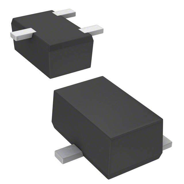
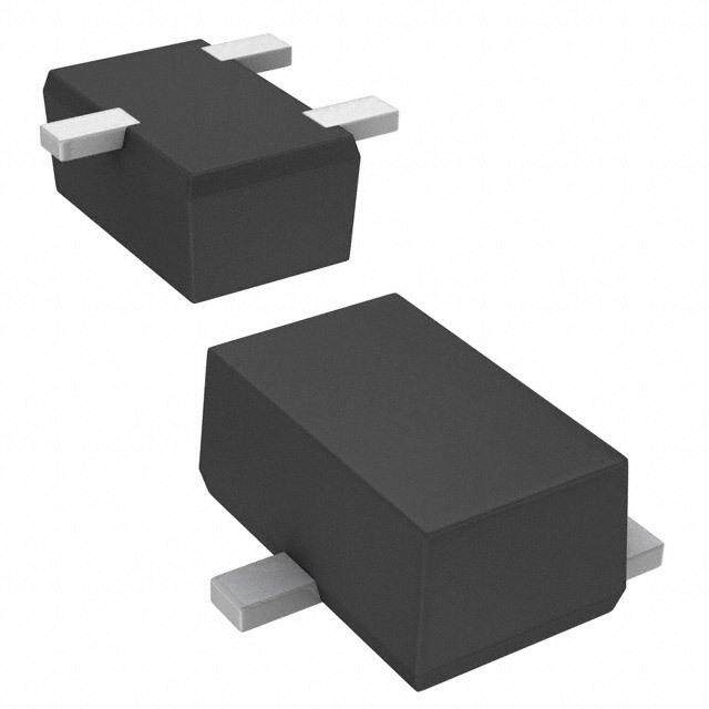
| 产品图片 |
|
| rohs | 符合RoHS无铅 / 符合限制有害物质指令(RoHS)规范要求 |
| 产品系列 | 晶体管,JFET,Panasonic DSK5J01Q0L- |
| 数据手册 | http://industrial.panasonic.com/www-cgi/jvcr13pz.cgi?E+SC+3+AJD7001+DSK5J01+8+WW |
| 产品型号 | DSK5J01Q0LDSK5J01Q0L |
| Pd-功率耗散 | 150 mW |
| Vgs-栅源极击穿电压 | - 55 V |
| Vgs=0时的漏-源电流 | 6.5 mA |
| 不同Id时的电压-截止(VGS关) | 5V @ 10µA |
| 不同Vds(Vgs=0)时的电流-漏极(Idss) | 2mA @ 10V |
| 不同Vds时的输入电容(Ciss) | 6pF @ 10V |
| 产品种类 | JFET |
| 供应商器件封装 | SMini3-F2-B |
| 其它名称 | DSK5J01Q0LDKR |
| 功率-最大值 | 150mW |
| 功率耗散 | 150 mW |
| 包装 | Digi-Reel® |
| 商标 | Panasonic |
| 安装类型 | 表面贴装 |
| 安装风格 | SMD/SMT |
| 封装 | Reel |
| 封装/外壳 | SC-85 |
| 封装/箱体 | SMini3-F2-B |
| 工厂包装数量 | 3000 |
| 晶体管极性 | N-Channel |
| 最大工作温度 | + 85 C |
| 最小工作温度 | - 40 C |
| 标准包装 | 1 |
| 正向跨导-最小值 | 2.5 mS |
| 漏极电流(Id)-最大值 | 30mA |
| 漏极电流Id-最大值 | 30 mA |
| 漏源极电压(Vdss) | 55V |
| 电压-击穿(V(BR)GSS) | - |
| 电阻-RDS(开) | - |
| 输入电容 | 6 pF |
| 配置 | Single |
| 闸/源击穿电压 | - 55 V |
| 闸/源截止电压 | - 5 V |


- 商务部:美国ITC正式对集成电路等产品启动337调查
- 曝三星4nm工艺存在良率问题 高通将骁龙8 Gen1或转产台积电
- 太阳诱电将投资9.5亿元在常州建新厂生产MLCC 预计2023年完工
- 英特尔发布欧洲新工厂建设计划 深化IDM 2.0 战略
- 台积电先进制程称霸业界 有大客户加持明年业绩稳了
- 达到5530亿美元!SIA预计今年全球半导体销售额将创下新高
- 英特尔拟将自动驾驶子公司Mobileye上市 估值或超500亿美元
- 三星加码芯片和SET,合并消费电子和移动部门,撤换高东真等 CEO
- 三星电子宣布重大人事变动 还合并消费电子和移动部门
- 海关总署:前11个月进口集成电路产品价值2.52万亿元 增长14.8%
PDF Datasheet 数据手册内容提取
Doc No. TT4-EA-12789 Revision. 2 Product Standards Junction FETs DSK5J010L DSK5J010L Silicon N-channel Junciton FET Unit: mm For low frequency amplificaton / For pyroelctric sensor DSK2J01 in SMini3 type package 2.0 0.3 0.13 Features 3 High gate-drain Voltage(Source open)VGDO Halogen-free / RoHS compliant (EU RoHS / UL-94 V-0 / MSL:Level 1 compliant) 1.252.1 1 2 Marking Symbol: B6 0.9 Packaging (0.65)(0.65) Embossed type (Thermo-compression sealing) : 3 000 pcs / reel (standard) 1.3 1. Source 2. Drain 3. Gate Panasonic SMini3-F2-B JEITA SC-85 Absolute Maximum Ratings Ta = 25 C Code ― Parameter Symbol Rating Unit Gate-drain voltage (Source short) VGDS -55 V Drain current ID 30 mA Internal Connection Gate current IG 10 mA (G) 3 Power dissipation PD 150 mW Channel temperature Tch 150 °C Operating ambient temperature Topr -40 to +85 °C Storage temperature Tstg -55 to +150 °C 1 2 (S) (D) Electrical Characteristics Ta = 25 C 3 C Parameter Symbol Conditions Min Typ Max Unit Gate-drain voltage (Source short) VGDS IG = -100 μA, VDS = 0 -55 V Drain current *1 IDSS VDS = 10 V , VGS = 0 1.0 12.0 mA Gate-source cutoff current IGSS VGS = -30 V, VDS = 0 -10 nA Gate-source cutoff voltage VGSC VDS = 10 V, ID = 10 μA -5 V Forward transfer admittance |Yfs| VDS = 10 V, ID = 5 mA, f =1 kHz 2.5 7.5 mS Small-signal short-circuit input capacitance Ciss 6.0 pF VDS = 10 V, VGS = 0, f = 1 MHz Small-signal reverse transfer capacitance Crss 2.5 pF Note) Measuring methods are based on JAPANESE INDUSTRIAL STANDARD JIS C 7030 Measuring methods for transistors. *1 Rank classification Code P Q R Rank P Q R IDSS (mA) 1.0 to 3.0 2.0 to 6.5 5.0 to 12.0 Marking symbol B6P B6Q B6R Page 1 of 3 Established :2010-10-26 Revised :2014-03-25
Doc No. TT4-EA-12789 Revision. 2 Product Standards Junction FETs DSK5J010L Technical Data ( reference ) PD-Ta ID-VGS 200 8 VDS = 10V -40 ℃ W)150 6 D (m mA) 25 ℃ ation P100 ent ID ( 4 sip urr s c wer Di 50 Drain 2 Ta = 85 ℃ o P 0 0 0 20 40 60 80 100 120 140 160 180 200 -1.5 -1 -0.5 0 0.5 Temperature Ta (℃) Gate-source voltage VGS (V) ID-VDS |Yfs|-ID 4 100 Ta= 25 ℃ Ta = 25 ℃ VGS= 0 V e 3 nc VDS = 10 V mA) mitta 10 ent ID ( 2 -0.2 V nsfer ads| (mS) ain curr 1 -0.4 V word tra|Yf 1 Dr or F -0.6 V 0 0.1 0 2 4 6 8 10 12 0.01 0.1 1 10 Drain-source voltage VDS (V) Drain current ID (mA) Cx-VDS 12 Ta= 25 ℃ 10 Ciss Coss F) 8 p e C ( 6 c n Crss a 4 cit a p a 2 C 0 0 5 10 15 20 Drain-source voltage VDS (V) Page 2 of 3 Established :2010-10-26 Revised :2014-03-25
Doc No. TT4-EA-12789 Revision. 2 Product Standards Junction FETs DSK5J010L SMini3-F2-B Unit: mm 2.0±0.2 +0.05 +0.05 0.13-0.02 0.30-0.02 3 0 1 1 . . 0 0 ± ± 5 1 2 . . 2 1 ) ° 5 1 2 ( 0 (0.65) (0.65) 05 . 0 ± 1.3±0.1 5 2 4 . 0 (5°) ) 9 4 9) 0.1 0. 8 ± ( (0. 0.9 1 . 0 o t 0 Land Pattern (Reference) (Unit: mm) 0.9 8 . 0 9 . 1 1.3 Page 3 of 3 Established :2010-10-26 Revised :2014-03-25
Request for your special attention and precautions in using the technical information and semiconductors described in this book (1) If anyof theproductsor technicalinformationdescribedinthisbook is tobe exported or provided to non-residents, the lawsandregulationsoftheexportingcountry,especially,thosewithregardtosecurityexportcontrol,mustbeobserved. (2)Thetechnicalinformationdescribedinthisbookisintendedonlytoshowthemaincharacteristicsandapplicationcircuit examples of the products. No license is granted in and to any intellectual property right or other right owned by Panasonic Corporation or any other company. Therefore, no responsibility is assumed by our company as to the infringement upon any such right owned by any other company which may arise as a result of the use of technical informationde-scribedinthisbook. (3) The products described in this book are intended to be used for general applications (such as office equipment, communicationsequipment,measuringinstrumentsandhouseholdappliances),orforspecificapplicationsasexpressly statedinthisbook. Please consult with our sales staff in advance for information on the following applications, moreover please exchange documentsseparatelyontermsofuseetc.:Specialapplications(suchasforin-vehicleequipment,airplanes,aerospace, automotive equipment, traffic signaling equipment, combustion equipment, medical equipment and safety devices) in which exceptional quality and reliability are required, or if the failure or malfunction of the products may directly jeopardizelifeorharmthehumanbody. Unlessexchangingdocumentsontermsofuseetc.inadvance,itistobeunderstoodthatourcompanyshallnotbeheld responsiblefor anydamageincurred asaresult of or inconnection with your usingthe productsdescribed inthisbook foranyspecialapplication. (4) The products and product specifications described in this book are subject to change without notice for modification and/orimprovement.Atthefinalstageofyourdesign,purchasing,oruseoftheproducts,therefore,askforthemostup- to-dateProductStandardsinadvancetomakesurethatthelatestspecificationssatisfyyourrequirements. (5) When designing your equipment, comply with the range of absolute maximum rating and the guaranteed operating conditions(operatingpowersupplyvoltageandoperatingenvironmentetc.).Especially,pleasebecarefulnottoexceed the range of absolute maximum rating on the transient state, such as power-on, power-off and mode-switching. Other- wise,wewillnotbeliableforanydefectwhichmayariselaterinyourequipment. Even when the products are used within the guaranteed values, take into the consideration of incidence of break down and failure mode, possible to occur to semiconductor products. Measures on the systems such as redundant design, arrestingthespreadoffireorpreventingglitcharerecommendedinordertopreventphysicalinjury,fire,socialdamages, forexample,byusingtheproducts. (6) Comply with the instructions for use in order to prevent breakdown and characteristics change due to external factors (ESD, EOS, thermal stress and mechanical stress) at the time of handling, mounting or at customer's process. We do notguaranteequalityfordisassembledproductsortheproductre-mountedafterremovingfromthemountingboard. Whenusingproductsforwhichdamp-proofpackingisrequired,satisfytheconditions,suchasshelflifeandtheelapsed timesincefirstopeningthepackages. (7) When reselling products described in this book to other companies without our permission and receiving any claim of requestfromtheresaledestination,pleaseunderstandthatcustomerswillbeartheburden. (8) This book may be not reprinted or reproduced whether wholly or partially, without the prior written permission of our company. No.010618