ICGOO在线商城 > 分立半导体产品 > 晶体管 - FET,MOSFET - 单 > STH180N10F3-6
 Datasheet下载
- 型号: STH180N10F3-6
- 制造商: STMicroelectronics
- 库位|库存: xxxx|xxxx
- 要求:
| 数量阶梯 | 香港交货 | 国内含税 |
| +xxxx | $xxxx | ¥xxxx |
查看当月历史价格
查看今年历史价格
STH180N10F3-6产品简介:
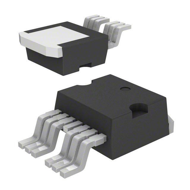
ICGOO电子元器件商城为您提供STH180N10F3-6由STMicroelectronics设计生产,在icgoo商城现货销售,并且可以通过原厂、代理商等渠道进行代购。 STH180N10F3-6价格参考。STMicroelectronicsSTH180N10F3-6封装/规格:晶体管 - FET,MOSFET - 单, 表面贴装 N 沟道 100V 180A(Tc) 315W(Tc) H2PAK-6。您可以下载STH180N10F3-6参考资料、Datasheet数据手册功能说明书,资料中有STH180N10F3-6 详细功能的应用电路图电压和使用方法及教程。
STMicroelectronics的STH180N10F3-6是一款N沟道MOSFET,属于晶体管 - FET,MOSFET - 单类别的产品。以下是其主要应用场景及特点:

 1. 电源管理
   - 开关电源(SMPS):适用于DC-DC转换器、降压或升压电路中,作为高效开关元件。
   - 负载开关:用于控制设备的供电路径,实现快速开启和关闭,降低功耗。
   - 电池管理系统:在电池充放电电路中,用作保护开关,防止过流、短路等异常情况。

 2. 电机驱动
   - 小型直流电机控制:用于低功率电机的启动、停止和速度调节。
   - H桥电路:在双向电机控制中,作为关键的开关器件。

 3. 工业应用
   - 继电器替代:由于其快速开关特性和低导通电阻(Rds(on)),可替代传统机械继电器,提高系统可靠性。
   - 工业自动化:用于传感器信号放大、执行器驱动等场景。

 4. 消费电子
   - 笔记本电脑和移动设备:在充电电路和电池保护电路中使用。
   - 音频设备:用于功率放大器中的开关或保护电路。

 5. 汽车电子
   - 车载电子设备:如车窗升降器、座椅调节器等低功率负载的驱动。
   - LED照明:用于汽车内外部LED灯的驱动电路。

 特点总结:
- 低导通电阻:Rds(on)典型值为18mΩ(@ Vgs=10V),有助于降低导通损耗,提高效率。
- 高电流能力:持续漏极电流可达18A(@ Tc=25°C),适合中高功率应用。
- 高耐压:最大漏源电压为100V,适用于多种电压等级的电路。
- 快速开关特性:低栅极电荷(Qg),支持高频开关应用。

这款MOSFET凭借其优异的性能和可靠性,广泛应用于需要高效功率转换和精确控制的场景中。
| 参数 | 数值 |
| 产品目录 | |
| 描述 | MOSFET N-CH 100V 180A H2PAKMOSFET N-ch 100V 3.9 Ohm 180A STripFET III |
| 产品分类 | FET - 单分离式半导体 |
| FET功能 | 标准 |
| FET类型 | MOSFET N 通道,金属氧化物 |
| Id-ContinuousDrainCurrent | 180 A |
| Id-连续漏极电流 | 180 A |
| 品牌 | STMicroelectronics |
| 产品手册 | |
| 产品图片 |
|
| rohs | 符合RoHS无铅 / 符合限制有害物质指令(RoHS)规范要求 |
| 产品系列 | 晶体管,MOSFET,STMicroelectronics STH180N10F3-6STripFET™ III |
| 数据手册 | |
| 产品型号 | STH180N10F3-6 |
| Pd-PowerDissipation | 315 W |
| Pd-功率耗散 | 315 W |
| RdsOn-Drain-SourceResistance | 4.5 mOhms |
| RdsOn-漏源导通电阻 | 4.5 mOhms |
| Vds-Drain-SourceBreakdownVoltage | 100 V |
| Vds-漏源极击穿电压 | 100 V |
| Vgs-Gate-SourceBreakdownVoltage | +/- 20 V |
| Vgs-栅源极击穿电压 | 20 V |
| 不同Id时的Vgs(th)(最大值) | 4V @ 250µA |
| 不同Vds时的输入电容(Ciss) | 6665pF @ 25V |
| 不同Vgs时的栅极电荷(Qg) | 114.6nC @ 10V |
| 不同 Id、Vgs时的 RdsOn(最大值) | 4.5 毫欧 @ 60A,10V |
| 产品种类 | MOSFET |
| 供应商器件封装 | H²PAK |
| 其它名称 | 497-11840-1 |
| 其它有关文件 | http://www.st.com/web/catalog/sense_power/FM100/CL824/SC1165/PF252303?referrer=70071840 |
| 功率-最大值 | 315W |
| 包装 | 剪切带 (CT) |
| 商标 | STMicroelectronics |
| 安装类型 | 表面贴装 |
| 安装风格 | SMD/SMT |
| 封装 | Reel |
| 封装/外壳 | TO-263-7,D²Pak(6 引线+接片) |
| 封装/箱体 | H2PAK-6 |
| 工厂包装数量 | 1000 |
| 晶体管极性 | N-Channel |
| 最大工作温度 | + 175 C |
| 最小工作温度 | - 55 C |
| 标准包装 | 1 |
| 漏源极电压(Vdss) | 100V |
| 电流-连续漏极(Id)(25°C时) | 180A (Tc) |
| 系列 | STH180N10F3-6 |
| 配置 | Single |


- 商务部:美国ITC正式对集成电路等产品启动337调查
- 曝三星4nm工艺存在良率问题 高通将骁龙8 Gen1或转产台积电
- 太阳诱电将投资9.5亿元在常州建新厂生产MLCC 预计2023年完工
- 英特尔发布欧洲新工厂建设计划 深化IDM 2.0 战略
- 台积电先进制程称霸业界 有大客户加持明年业绩稳了
- 达到5530亿美元!SIA预计今年全球半导体销售额将创下新高
- 英特尔拟将自动驾驶子公司Mobileye上市 估值或超500亿美元
- 三星加码芯片和SET,合并消费电子和移动部门,撤换高东真等 CEO
- 三星电子宣布重大人事变动 还合并消费电子和移动部门
- 海关总署:前11个月进口集成电路产品价值2.52万亿元 增长14.8%


PDF Datasheet 数据手册内容提取
STH180N10F3-6 N-channel 100 V, 3.9 mΩ typ.,180 A, STripFET™ F3 Power MOSFET in H²PAK-6 package Datasheet - production data Features ) TAB Order code VDS RmDaS(xon. ) ( sID t c STH180N10F3-6 100 V 4.u5 mΩ 180 A 7 d o 1 Low on-resistencer R P DS(on) 100% avalanche tested 2 e H PAK-6 t Applicaetions l o Figure 1: Internal schematic diagram Switching applications s b O Description - This device is an N-channel Power MOSFET ) developed using STripFET™ F3 technology. It is s ( designed to minimize on-resistance and gate t c charge to provide superior switching u performance. d o Table 1: Device summary r P Order code Marking Package Packing e Tape STH180N10F3-6 180N10F3 H2PAK-6 e t and reel l S(2,3,4,5,6,7) o s b O November 2014 DocID022347 Rev 4 1/15 This is information on a product in full production. www.st.com
Contents STH180N10F3-6 Contents 1 Electrical ratings ............................................................................. 3 2 Electrical characteristics ................................................................ 4 2.1 Electrical characteristics (curves) ...................................................... 6 3 Test circuits ..................................................................................... 8 4 Package information ....................................................................... 9 4.1 H2PAK-6 package information ........................................................... 9 4.2 Packing information ......................................................................... 12 ) s 5 Revision history ...................................................................(......... 14 t c u d o r P e t e l o s b O - ) s ( t c u d o r P e t e l o s b O 2/15 DocID022347 Rev 4
STH180N10F3-6 Electrical ratings 1 Electrical ratings Table 2: Absolute maximum ratings Symbol Parameter Value Unit V Drain-source voltage 100 V DS V Gate-source voltage ± 20 V GS I (1) Drain current (continuous) at T = 25 °C 180 A D C I (1) Drain current (continuous) at T = 100 °C 120 A D C I (2) Drain current (pulsed) 720 A DM Total dissipation at T = 25 °C 315 W P C ) TOT s Derating factor 2.1 W/ºC ( t dv/dt Peak diode recovery voltage slope 20 c V/ns u EAS(3) Single pulse avalanche energy 350 d mJ o T Operating junction temperature °C J -55 to 1r75 P T Storage temperature °C stg e Notes: t e (1)Current limited by package l o (2)Pulse width limited by safe operating area s (3)Starting TJ = 25 °C, ID = 80, VDD = 50 V O b - Table 3: Thermal resistance ) s Symbol Parameter Value Unit ( t R Thermal recsistance junction-case 0.48 °C/W thj-case u R (1) Thedrmal resistance junction-pcb 35 °C/W thj-pcb o r Notes: P (1)Wh en mounted on FR-4 board of 1 inch², 2 oz Cu e t e l o s b O DocID022347 Rev 4 3/15
Electrical characteristics STH180N10F3-6 2 Electrical characteristics (T = 25 °C unless otherwise specified) CASE Table 4: On/off-state Symbol Parameter Test conditions Min. Typ. Max. Unit Drain-source breakdown V I = 250 µA 100 V (BR)DSS voltage (VGS= 0) D V = 100 V 10 µA DS Zero gate voltage drain IDSS current (VGS = 0) VDS = 100 V; 100 µA TC = 125 °C ) Gate body leakage current s I V = ±20 V ±200 nA GSS GS ( (VDS = 0) t c VGS(th) Gate threshold voltage VDS = VGS, ID = 250 µA 2 u 4 V d Static drain-source on- R V = 10 V, I = 60 A o 3.9 4.5 mΩ DS(on) resistance GS D r P e Table 5: Dynamic t e Symbol Parameter Test conditions Min. Typ. Max. Unit l o Ciss Input capacitance s 6665 pF b Coss Output capacitance VODS = 25 V, f = 1 MHz, 786 pF V = 0 Reverse transfer GS Crss capacitance - 49 pF ) - - s Q Total gate charge V = 50 V, I = 120 A 114.6 nC g ( DD D Qgs Gate-sourcec ctharge VGS = 10 V 38.8 nC u See Figure 14: "Gate Qgd Gate-ddrain charge charge test circuit" 31.9 nC o r P Table 6: Switching times e tSymbol Parameter Test conditions Min. Typ. Max. Unit e l t Turn-on delay time V = 50 V, I = 60 A, 25.6 ns o d(on) DD D s tr Rise time RG = 4.7 Ω, VGS= 10 V 97.1 ns b See Figure 13: - - O td(off) Turn-off delay time "Switching times test 99.9 ns tf Fall time circuit for resistive load" 6.9 ns 4/15 DocID022347 Rev 4
STH180N10F3-6 Electrical characteristics Table 7: Source-drain diode Symbol Parameter Test conditions Min. Typ. Max. Unit I Source-drain current 180 A SD I (1) Source-drain current (pulsed) 720 A SDM V (2) Forward on voltage I = 120 A, V = 0 1.5 V SD SD GS - t Reverse recovery time I = 120 A, 83.4 ns rr SD Q Reverse recovery charge di/dt = 100 A/µs, 295.7 nC rr V = 80 V, T= 150 DD j IRRM Reverse recovery current °C 7.1 A Notes: (1)Pulse width limited by safe operating area ) (2)Pulsed: pulse duration = 300 µs, duty cycle 1.5% s ( t c u d o r P e t e l o s b O - ) s ( t c u d o r P e t e l o s b O DocID022347 Rev 4 5/15
Electrical characteristics STH180N10F3-6 2.1 Electrical characteristics (curves) Figure 3: Thermal impedance Figure 2: Safe operating area 280tok ID GIPG110620141143SA K (A) ᵟ=0.5 11000 OpLeiramtiitoend ibn yt himsa xa rRea iDsS(on) 10ms 10-1 0.01.2 0.05 0.02 Zth=k Rthj-c 1 0.01 ᵟ=tp/t 1ms Tj=175°C 0.1 STcin=g2le5 °pCulse 100µs Single pulse tpt s ) 0.1 1 10 VDS(V) 101-20-5 10-4 10-3 10-2 c1t0-1( tp(s) u d o Figure 5: Transfer characteristics Figure 4: Output characteristics r P AM08617v1 ID(A) VGS=10V AM08616v1 ID(A) e 350 350t VDS=2V 7V e 300 l300 o 250 s 250 b 200 O 200 150 - 6V 150 100 s ) 100 ( 50 t 50 c 5V 0 u 0 1 2d 3 4 5 6 7 8 VDS(V) 00 1 2 3 4 5 6 7 8 9 VGS(V) o r P Figure 6: Normalized V(BR)DSS vs Figure 7: Static drain-source on-resistance e t temperature RDS(on) AM08626v1 e V(BR)DSS AM08618v1 (mΩ) l (norm) VGS=10V o ID=1mA 4.2 s 1.10 b 4.1 O 1.05 4.0 3.9 1.00 3.8 0.95 3.7 0.90 3.6 -75 -25 25 75 125 175 TJ(°C) 0 20 40 60 80 100 120140160180 ID(A) 6/15 DocID022347 Rev 4
STH180N10F3-6 Electrical characteristics Figure 8: Gate charge vs gate-source Figure 9: Capacitance variations voltage C AM08621v1 VGS AM08620v1 (pF) (V) VDD=50V 12 ID=120A 20000 10 15000 8 6 10000 4 Ciss 5000 2 Crss Coss 0 0 0 20 40 60 80 100 120 140 Qg(nC) 0 20 40 60 80 100 )VDS(V) s ( t c Figure 11: Normalized on-uresistance vs Figure 10: Normalized gate threshold temperatdure voltage vs temperature o VGS(th) AM08622v1 RD(nSo(ormn)) P r AM08623v1 (norm) ID=250µA 2.1 ID=60A 1.3 e VGS=10V 1.t9 e 1.1 l1.7 o s 1.5 0.9 b O 1.3 0.7 1.1 - 0.5 s ) 0.9 ( 0.7 0.3 ct -75 -25 2u5 75 125 175 TJ(°C) 0.5-75 -25 25 75 125 175 TJ(°C) d o r P Figure 12: Source-drain diode forward characteristics e VSD AM08624v1 t (V) e ol 1.0 TJ=-55°C s b 0.9 O 0.8 0.7 TJ=25°C 0.6 0.5 TJ=175°C 0.4 0 20 40 60 80 100 120 ISD(A) DocID022347 Rev 4 7/15
Test circuits STH180N10F3-6 3 Test circuits Figure 13: Switching times test circuit for resistive Figure 14: Gate charge test circuit load VDD 12 V 47 kΩ 1 kΩ 100 nF Vi ≤ VGS IG= CONST 100 Ω D.U.T. 2.7 kΩ VG 2200 μF ) 47 kΩ s ( t 1 kΩ c PW u d AM01469v1 o r P e Figure 15: Test circuit for inductive load Figure t16: Unclamped inductive load test circuit switching and diode recovery times e l o s b O - ) s ( t c u d o r P e t e l o Figure 17: Unclamped inductive waveform Figure 18: Switching time waveform s b V(BR)DSS ton toff O td(on) tr td(off) tf V D 90% 90% I DM 10% ID 0 10% VDS VDD VDD 90% V GS AM01472v1 0 10% AM01473v1 8/15 DocID022347 Rev 4
STH180N10F3-6 Package information 4 Package information In order to meet environmental requirements, ST offers these devices in different grades of ECOPACK® packages, depending on their level of environmental compliance. ECOPACK® specifications, grade definitions and product status are available at: www.st.com. ECOPACK® is an ST trademark. 4.1 H2PAK-6 package information Figure 19: H²PAK-6 outline ) s ( t c u d o r P e t e l o s b O - ) s ( t c u d o r P e t e l o s b O 8159693_Rev_F DocID022347 Rev 4 9/15
Package information STH180N10F3-6 Table 8: H²PAK-6 mechanical data mm Dim. Min. Typ. Max. A 4.30 4.80 A1 0.03 0.20 C 1.17 1.37 e 2.34 2.74 e1 4.88 5.28 e2 7.42 7.82 E 0.45 0.60 F 0.50 0.70 ) s H 10.00 10.(40 t - c H1 7.40 u 7.80 d L 14.75 15.25 o L1 1.27 r 1.40 P L2 4.35 4.95 e L3 6.85 t 7.25 e L4 1.5 l 1.75 o M 1.90 s 2.50 b R 0.20 O 0.60 V 0-° 8° ) s ( t c u d o r P e t e l o s b O 10/15 DocID022347 Rev 4
STH180N10F3-6 Package information Figure 20: H²PAK-6 recommended footprint ) s ( t c u d o r P e t e l o s b O - ) s ( t c u d o r P e t e l o s b footprint_Rev_F O Dimensions are in mm. DocID022347 Rev 4 11/15
Package information STH180N10F3-6 4.2 Packing information Figure 21: Tape outline ) s ( t c u d o r P e t e l o s b O - ) s ( t c u d o Figure 22: Reel outline r P T REELDIMENSIONS e t 40 mm min. e l o Accesshole s b Atslot location O B D C N A Gmeasured Tape slot Incore for Fullradius Athub Tape start 12/15 DocID022347 Rev 4
STH180N10F3-6 Package information Table 9: Tape and reel mechanical data Tape Reel mm mm Dim. Dim. Min. Max. Min. Max. A0 10.5 10.7 A 330 B0 15.7 15.9 B 1.5 D 1.5 1.6 C 12.8 13.2 D1 1.59 1.61 D 20.2 E 1.65 1.85 G 24.4 26.4 F 11.4 11.6 N 100 K0 4.8 5.0 T 30).4 s P0 3.9 4.1 t( c P1 11.9 12.1 Base quantity u 1000 d P2 1.9 2.1 Bulk quantity 1000 o R 50 r P T 0.25 0.35 e W 23.7 24.3 t e l o s b O - ) s ( t c u d o r P e t e l o s b O DocID022347 Rev 4 13/15
Revision history STH180N10F3-6 5 Revision history Table 10: Document revision history Date Revision Changes 10-Oct-2011 1 First version Updated features in cover page 04-Nov-2011 2 Updated: H2PAK-6 package mechanical data. Updated: title, features and description. 14-Nov-2014 3 Minor text changes. 26-Nov-2014 4 Updated Table 4: "On/off-state". ) s ( t c u d o r P e t e l o s b O - ) s ( t c u d o r P e t e l o s b O 14/15 DocID022347 Rev 4
STH180N10F3-6 IMPORTANT NOTICE – PLEASE READ CAREFULLY STMicroelectronics NV and its subsidiaries (“ST”) reserve the right to make changes, corrections, enhancements, modifications, and improvements to ST products and/or to this document at any time without notice. Purchasers should obtain the latest relevant information on ST products before placing orders. ST products are sold pursuant to ST’s terms and conditions of sale in place at the time of order acknowledgement. Purchasers are solely responsible for the choice, selection, and use of ST products and ST assumes no liability for application assistance or the design of Purchasers’ products. ) No license, express or implied, to any intellectual property right is granted by ST herein. s ( t c u Resale of ST products with provisions different from the information set forth herein shall void any warranty granted by ST for such product. d o r P ST and the ST logo are trademarks of ST. All other product or service names are the property of their respective owners. e t e Information in this document supersedes and replaces information previously supplied inl any prior versions of this document. o s b © 2014 STMicroelectronOics – All rights reserved - ) s ( t c u d o r P e t e l o s b O DocID022347 Rev 4 15/15