ICGOO在线商城 > 分立半导体产品 > 晶体管 - FET,MOSFET - 阵列 > SI6924AEDQ-T1-E3

 Datasheet下载
- 型号: SI6924AEDQ-T1-E3
- 制造商: Vishay
- 库位|库存: xxxx|xxxx
- 要求:
| 数量阶梯 | 香港交货 | 国内含税 |
| +xxxx | $xxxx | ¥xxxx |
查看当月历史价格
查看今年历史价格
SI6924AEDQ-T1-E3产品简介:
ICGOO电子元器件商城为您提供SI6924AEDQ-T1-E3由Vishay设计生产,在icgoo商城现货销售,并且可以通过原厂、代理商等渠道进行代购。 SI6924AEDQ-T1-E3价格参考。VishaySI6924AEDQ-T1-E3封装/规格:晶体管 - FET,MOSFET - 阵列, Mosfet Array 2 N-Channel (Dual) Common Drain 28V 4.1A 1W Surface Mount 8-TSSOP。您可以下载SI6924AEDQ-T1-E3参考资料、Datasheet数据手册功能说明书,资料中有SI6924AEDQ-T1-E3 详细功能的应用电路图电压和使用方法及教程。
Vishay Siliconix 的 SI6924AEDQ-T1-E3 是一款双通道 N 沟道 MOSFET 阵列,采用先进的沟槽技术制造,具有低导通电阻(RDS(on))和高效率特性。该器件广泛应用于对空间和能效要求较高的电子系统中。

典型应用场景包括:便携式电子设备(如智能手机、平板电脑和笔记本电脑)中的电源管理与负载开关,用于高效控制电池供电路径;在DC-DC转换器中作为同步整流开关,提升电源转换效率;在电机驱动电路中实现小型直流电机或步进电机的控制;还可用于热插拔控制器、LED驱动电路以及各类低电压、大电流开关应用。

SI6924AEDQ-T1-E3 支持低栅极电压驱动(1.8V至2.5V),适用于现代低压逻辑控制环境,兼容微控制器直接驱动,无需额外电平转换。其小尺寸的PowerPAK® SC-70封装节省PCB空间,适合高密度布局设计。

此外,该器件具备良好的热稳定性与可靠性,工作温度范围宽(-55°C 至 +150°C),适用于工业控制、消费电子及便携医疗设备等多种环境。由于其双MOSFET结构,还可用于H桥电路或信号切换应用,提供灵活的设计方案。
| 参数 | 数值 |
| 产品目录 | |
| 描述 | MOSFET 2N-CH 28V 4.1A 8-TSSOP |
| 产品分类 | FET - 阵列 |
| FET功能 | 逻辑电平门 |
| FET类型 | 2 N 沟道(双)共漏 |
| 品牌 | Vishay Siliconix |
| 数据手册 | |
| 产品图片 |
|
| 产品型号 | SI6924AEDQ-T1-E3 |
| rohs | 无铅 / 符合限制有害物质指令(RoHS)规范要求 |
| 产品系列 | - |
| 不同Id时的Vgs(th)(最大值) | 1.5V @ 250µA |
| 不同Vds时的输入电容(Ciss) | - |
| 不同Vgs时的栅极电荷(Qg) | 10nC @ 4.5V |
| 不同 Id、Vgs时的 RdsOn(最大值) | 33 毫欧 @ 4.6A,4.5V |
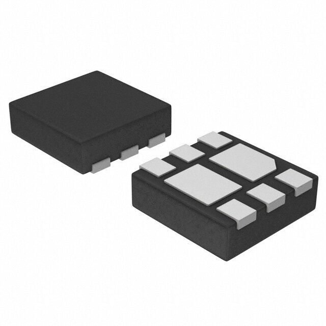
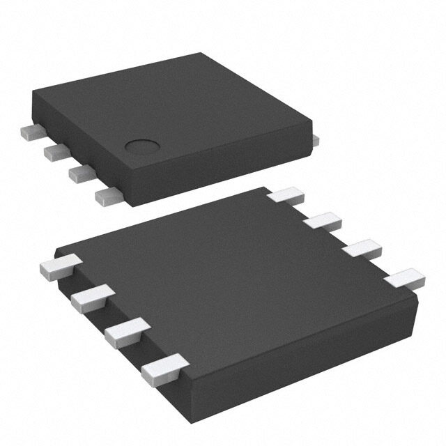
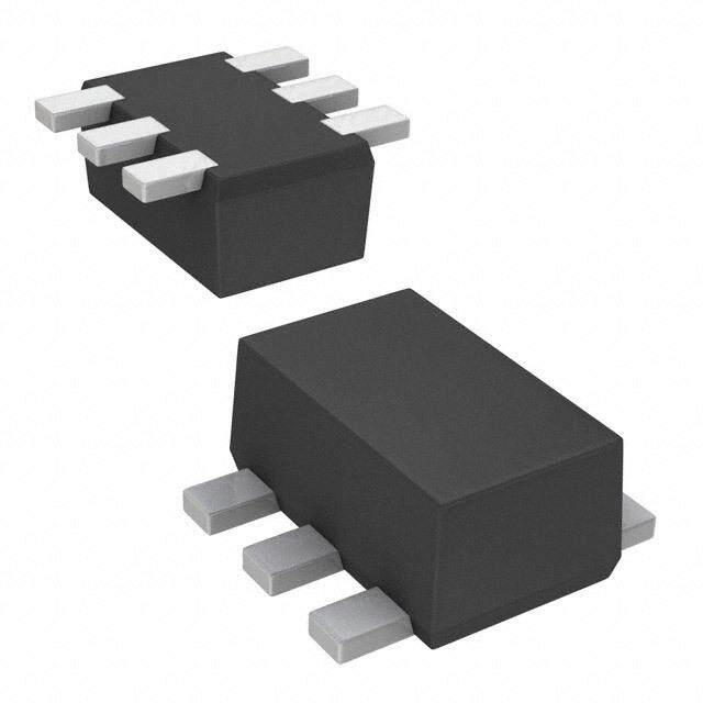
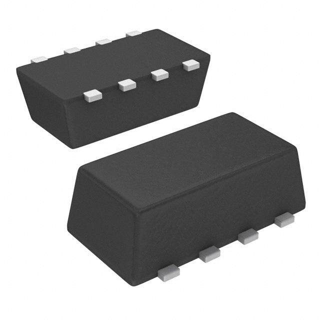
| 供应商器件封装 | 8-TSSOP |
| 其它名称 | SI6924AEDQ-T1-E3CT |
| 功率-最大值 | 1W |
| 包装 | 剪切带 (CT) |
| 安装类型 | 表面贴装 |
| 封装/外壳 | 8-TSSOP(0.173",4.40mm 宽) |
| 标准包装 | 1 |
| 漏源极电压(Vdss) | 28V |
| 电流-连续漏极(Id)(25°C时) | 4.1A |


.jpg)
PDF Datasheet 数据手册内容提取
Si6924AEDQ Vishay Siliconix N-Channel 2.5-V (G-S) Battery Switch, ESD Protection FEATURES PRODUCT SUMMARY • Halogen-free V (V) R (Ω) I (A) DS DS(on) D (cid:129) Low R 0.033 at VGS = 4.5 V 4.6 DS(on) (cid:129) VGS Max Rating: 14 V RoHS 28 0.038 at VGS = 3.0 V 4.3 (cid:129) Exceeds 2 kV ESD Protection COMPLIANT 0.042 at VGS = 2.5 V 4.1 (cid:129) 28 V V Rated DS (cid:129) Symmetrical Voltage Blocking (Off Voltage) DESCRIPTION The Si6924AEDQ is a dual N-Channel MOSFET with ESD stage diode is designed to protect the gate from any protection and gate over-voltage protection circuitry remaining ESD energy and over-voltages above the gates incorporated into the MOSFET. The device is designed for inherent safe operating range. The series resistor used to use in Lithium Ion battery pack circuits. The common-drain limit the current through the second stage diode during over construction takes advantage of the typical battery pack voltage conditions has a maximum value which limits the topology, allowing a further reduction of the device’s on- input current to ≤ 10 mA at 14 V and the maximum t to 12 off resistance. The 2-stage input protection circuit is a unique µs. The Si6924AEDQ has been optimized as a battery or design, consisting of two stages of back-to-back zener load switch in Lithium Ion applications with the advantage of diodes separated by a resistor. The first stage diode is both a 2.5 V R rating and a safe 14 V gate-to-source DS(on) designed to absorb most of the ESD energy. The second maximum rating. APPLICATION CIRCUITS D ESD and ESD and Overvoltage Overvoltage Protection Protection R** G S Battery Protection Circuit **R typical value is 3.3 kΩ by design. See Typical Characteristics, *Thermal connection to drain pins is required to achieve specific performance Gate-Current vs. Gate-Source Voltage, Page 3. Figure 1. Typical Use In a Lithium Ion Battery Pack Figure 2. Input ESD and Overvoltage Protection Circuit Document Number: 72215 www.vishay.com S-81056-Rev. B, 12-May-08 1
Si6924AEDQ Vishay Siliconix FUNCTIONAL BLOCK DIAGRAM AND PIN CONFIGURATION *D *D 3.3 kΩ 3.3 kΩ TSSOP-8 G1 G2 D 1 8 D S1 2 Si6924AEDQ 7 S2 S1 3 6 S2 G1 4 5 G2 S1 S2 Top View N-Channel N-Channel Ordering Information:Si6924AEDQ-T1-GE3 (Lead (Pb)-free and Halogen-free) *Thermal connection to drain pins is required to achieve specific performance. Figure 3. Figure 4. ABSOLUTE MAXIMUM RATINGS T = 25 °C, unless otherwise noted A Parameter Symbol 10 s Steady State Unit Drain-Source Voltage, Source-Drain Voltage VDS 28 V Gate-Source Voltage VGS ± 14 Continuous Drain-to-Source Current (TJ = 150 °C)a TTAA == 2750 °°CC ID 43..67 43..12 A Pulsed Drain-to-Source Current IDM 20 Pulsed Source Current (Diode Conduction)a IS 1.2 0.9 TA = 25 °C 1.3 1.0 Maximum Power Dissipationa PD W TA = 70 °C 0.84 0.64 Operating Junction and Storage Temperature Range TJ, Tstg - 55 to 150 °C THERMAL RESISTANCE RATINGS Parameter Symbol Typical Maximum Unit t ≤ 10 s 71 95 Maximum Junction-to-Ambienta RthJA Steady State 96 125 °C/W Maximum Junction-to-Foot (Drain) Steady State RthJF 56 70 Notes: a. Surface Mounted on FR4 board. www.vishay.com Document Number: 72215 2 S-81056-Rev. B, 12-May-08
Si6924AEDQ Vishay Siliconix SPECIFICATIONS T = 25 °C, unless otherwise noted J Parameter Symbol Test Conditions Min. Typ. Max. Unit Static Gate Threshold Voltage VGS(th) VDS = VGS, ID = 250 µA 0.6 1.5 V VDS = 0 V, VGS = ± 4.5 V ± 1 µA Gate-Body Leakage IGSS VDS = 0 V, VGS = ± 14 V ± 20 mA VDS = 22.4 V, VGS = 0 V 1 Zero Gate Voltage Drain Current IDSS µA VDS = 22.4 V, VGS = 0 V, TJ = 55 °C 5 On-State Drain Currentb ID(on) VDS ≥ 5 V, VGS = 5 V 10 A VGS = 4.5 V, ID = 4.6 A 0.022 0.033 Drain-Source On-State Resistanceb RDS(on) VGS = 3.0 V, ID = 4.3 A 0.025 0.038 Ω VGS = 2.5 V, ID = 4.1 A 0.029 0.042 Forward Transconductanceb gfs VDS = 10 V, ID = 4.6 A 25 S Diode Forward Voltageb VSD IS = 1.2 A, VGS = 0 V 0.7 1.1 V Dynamica Total Gate Charge Qg 6.5 10 Gate-Source Charge Qgs VDS = 10 V, VGS = 4.5 V, ID = 4.6 A 1.2 nC Gate-Drain Charge Qgd 1.5 Turn-On Delay Time td(on) 0.95 1.5 Rise Time tr VDD = 10 V, RL = 10 Ω 1.4 2.1 µs Turn-Off Delay Time td(off) ID ≅ 1 A, VGEN = 4.5 V, RG = 6 Ω 7 11 Fall Time tf 3.1 5 Notes: a. Guaranteed by design, not subject to production testing. b. Pulse test; pulse width ≤ 300 µs, duty cycle ≤ 2 %. Stresses beyond those listed under “Absolute Maximum Ratings” may cause permanent damage to the device. These are stress ratings only, and functional operation of the device at these or any other conditions beyond those indicated in the operational sections of the specifications is not implied. Exposure to absolute maximum rating conditions for extended periods may affect device reliability. TYPICAL CHARACTERISTICS 25°C, unless otherwise noted 0.020 10,000 1,000 mA) 0.015 A) 100 Current ( Current ( 10 TJ = 150 °C Gate 0.010 Gate 1 - - S S GS GS 0.1 I 0.005 I TJ = 25 °C 0.01 0.000 0.001 0 3 6 9 12 15 0 2 4 6 8 10 12 14 VGS - Gate-to-Source Voltage (V) VGS -Gate-to-Source Voltage (V) Gate-Current vs. Gate-Source Voltage Gate Current vs. Gate-Source Voltage Document Number: 72215 www.vishay.com S-81056-Rev. B, 12-May-08 3
Si6924AEDQ Vishay Siliconix TYPICAL CHARACTERISTICS 25°C, unless otherwise noted 25 25 VGS = 5 thru 2,5 V 20 20 - Drain Current (A)D 1105 2 V - Drain Current (A)D 1105 I I TC = 125 °C 5 5 25 °C - 55 °C 0 0 0.00 0.25 0.50 0.75 1.00 1.25 1.50 0.0 0.5 1.0 1.5 2.0 2.5 3.0 VDS - Drain-to-Source Voltage (V) VGS - Gate-to-Source Voltage (V) Output Characteristics Transfer Characteristics 0.05 5 )Ω 0.04 ge (V) 4 IVDD =S 4=. 61 0A V nce ( Volta sta 0.03 VGS = 2.5 V ce 3 Resi Sour n- o- - OS(on) 0.02 VGS = 3 V VGS = 4.5 V - Gate-t 2 RD 0.01 GS 1 V 0.00 0 0 4 8 12 16 20 0 1 2 3 4 5 6 7 ID - Drain Current (A) Qg - Total Gate Charge (nC) On-Resistance vs. Drain Current Gate Charge 1.8 20 VGS = 4.5 V 1.6 ID = 4.6 A 10 e - On-ResistancRDS(on)(Normalized) 111...024 - Source Current (A)S TJ = 150 °C TJ = 25 °C I 0.8 0.6 1 - 50 - 25 0 25 50 75 100 125 150 0 0.4 0.6 0.8 1.0 1.2 TJ - Junction Temperature (°C) VSD - Source-to-Drain Voltage (V) On-Resistance vs. Junction Temperature Source-Drain Diode Forward Voltage www.vishay.com Document Number: 72215 4 S-81056-Rev. B, 12-May-08
Si6924AEDQ Vishay Siliconix TYPICAL CHARACTERISTICS 25°C, unless otherwise noted 0.10 0.4 ID = 250 µA 0.08 0.2 )Ω e ( V) Resistanc 0.06 IIDD == 44..66 AA Variance ( 0.0 - On-on) 0.04 VGS(th) -0.2 S( D R 0.02 -0.4 0.00 -0.6 0 1 2 3 4 5 - 50 - 25 0 25 50 75 100 125 150 VVGS -- GGaattee--ttoo--SSoouurrccee VVoollttaaggee ((VV)) TJ - Temperature (°C) On-Resistance vs. Gate-to-Source Voltage Threshold Voltage 100 60 Limited by R D S (o n )* 50 10 40 A) 1 ms W) ent ( er ( 30 Curr 1 Pow ain 10 ms Dr 20 - 100 ms D I 0.1 TC = 25 °C 1 s 10 Single Pulse 10 s DC 0 0.01 0.001 0.01 0.1 1 10 0.1 1 10 100 Time (s) VD S -Drain-to-SourceVoltage(V) Single Pulse Power *VGS>minimumVGSatwhichRDS(on)isspecified Safe Operating Area 2 1 nt Duty Cycle = 0.5 e ed Effective Transiermal Impedance 0.1 000...2105 NPoDteMs: NormalizTh 0.02 1. Duty Cytc1le, tD2 = tt12 2. Per Unit Base = RthJA = 96 °C/W 3. TJM - TA = PDMZthJA(t) Single Pulse 4. Surface Mounted 0.01 10-4 10-3 10-2 10-1 1 10 100 600 Square Wave Pulse Duration (s) Normalized Thermal Transient Impedance, Junction-to-Ambient Document Number: 72215 www.vishay.com S-81056-Rev. B, 12-May-08 5
Si6924AEDQ Vishay Siliconix TYPICAL CHARACTERISTICS 25°C, unless otherwise noted 2 1 nt Duty Cycle = 0.5 e ctive Transimpedance 0.2 zed Effehermal I 0.1 00..105 aliT m or 0.02 N Single Pulse 0.01 10-4 10-3 10-2 10-1 1 10 Square Wave Pulse Duration (s) Normalized Thermal Transient Impedance, Junction-to-Foot Vishay Siliconix maintains worldwide manufacturing capability. Products may be manufactured at one of several qualified locations. Reliability data for Silicon Technology and Package Reliability represent a composite of all qualified locations. For related documents such as package/tape drawings, part marking, and reliability data, see http://www.vishay.com/ppg?72215. www.vishay.com Document Number: 72215 6 S-81056-Rev. B, 12-May-08
Legal Disclaimer Notice www.vishay.com Vishay Disclaimer ALL PRODUCT, PRODUCT SPECIFICATIONS AND DATA ARE SUBJECT TO CHANGE WITHOUT NOTICE TO IMPROV E RELIABILITY, FUNCTION OR DESIGN OR OTHERWISE. Vishay Intertechnology, Inc., its affiliates, agents, and employees, and all persons acting on its or their behalf (collectively, “Vishay”), disclaim any and all liability for any errors, inaccuracies or incompleteness contained in any datasheet or in any other disclosure relating to any product. Vishay makes no warranty, representation or guarantee regarding the suitability of the products for any particular purpose o r the continuing production of any product. To the maximum extent permitted by applicable law, Vishay disclaims (i) any and all liability arising out of the application or use of any product, (ii) any and all liability, including without limitation special, consequential or incidental damages, and (iii) any and all implied warranties, including warranties of fitness for particular purpose, non-infringement and merchantability. Statements regarding the suitability of products for certain types of applications are based on Vishay’s knowledge of typical requirements that are often placed on Vishay products in generic applications. Such statements are not binding statements about the suitability of products for a particular application. It is the customer’s responsibility to validate that a particular product with the properties described in the product specification is suitable for use in a particular application. Parameters provided in datasheets and / or specifications may vary in different applications and performance may vary over time. All operating parameters, including typical parameters, must be validated for each customer application by the customer’s technical experts. Product specifications do not expand or otherwise modify Vishay’s terms and conditions of purchase, including but not limited to the warranty expressed therein. Except as expressly indicated in writing, Vishay products are not designed for use in medical, life-saving, or life-sustainin g applications or for any other application in which the failure of the Vishay product could result in personal injury or death. Customers using or selling Vishay products not expressly indicated for use in such applications do so at their own risk . Please contact authorized Vishay personnel to obtain written terms and conditions regarding products designed for such applications. No license, express or implied, by estoppel or otherwise, to any intellectual property rights is granted by this documen t or by any conduct of Vishay. Product names and markings noted herein may be trademarks of their respective owners. © 2021 VISHAY INTERTECHNOLOGY, INC. ALL RIGHTS RESERVED Revision: 01-Jan-2021 1 Document Number: 91000