ICGOO在线商城 > 分立半导体产品 > 晶体管 - FET,MOSFET - 单 > PSMN8R5-60YS,115
 Datasheet下载
- 型号: PSMN8R5-60YS,115
- 制造商: NXP Semiconductors
- 库位|库存: xxxx|xxxx
- 要求:
| 数量阶梯 | 香港交货 | 国内含税 |
| +xxxx | $xxxx | ¥xxxx |
查看当月历史价格
查看今年历史价格
PSMN8R5-60YS,115产品简介:
ICGOO电子元器件商城为您提供PSMN8R5-60YS,115由NXP Semiconductors设计生产,在icgoo商城现货销售,并且可以通过原厂、代理商等渠道进行代购。 PSMN8R5-60YS,115价格参考。NXP SemiconductorsPSMN8R5-60YS,115封装/规格:晶体管 - FET,MOSFET - 单, 表面贴装 N 沟道 60V 76A(Tc) 106W(Tc) LFPAK56,Power-SO8。您可以下载PSMN8R5-60YS,115参考资料、Datasheet数据手册功能说明书,资料中有PSMN8R5-60YS,115 详细功能的应用电路图电压和使用方法及教程。
PSMN8R5-60YS,115 是 Nexperia USA Inc. 生产的一款单通道 MOSFET(金属氧化物场效应晶体管),属于 FET 晶体管类别。这款 MOSFET 的主要应用场景如下:

 1. 电源管理
该器件适用于各种电源管理系统,特别是在需要高效能、低损耗的场合。它具有较低的导通电阻(Rds(on)),能够有效减少功率损耗,提升电源转换效率。常见的应用包括开关电源(SMPS)、DC-DC 转换器、电池管理系统(BMS)等。

 2. 电机控制
在电机驱动和控制系统中,PSMN8R5-60YS,115 可用于驱动直流电机、步进电机或无刷直流电机。其快速开关特性和低导通电阻有助于提高电机的响应速度和效率,同时降低发热,延长设备寿命。

 3. 负载开关
作为负载开关,该 MOSFET 可以实现对电路中不同负载的精确控制。例如,在智能手机、平板电脑等便携式电子设备中,MOSFET 用于管理电池与各个功能模块之间的电力分配,确保系统稳定运行并节省电能。

 4. 保护电路
该器件还可以用于过流保护、短路保护等安全电路设计中。通过检测电流的变化,MOSFET 可以迅速切断异常电流路径,防止电路损坏,保障系统的安全性。

 5. 汽车电子
在汽车电子领域,PSMN8R5-60YS,115 广泛应用于车载充电器、电动助力转向系统(EPS)、车身控制模块(BCM)等部件中。其高可靠性和耐高温性能使其能够在恶劣的车用环境中稳定工作。

 6. 工业自动化
在工业自动化设备中,如可编程逻辑控制器(PLC)、伺服驱动器等,该 MOSFET 可用于信号传输、传感器接口及执行机构的驱动,确保工业设备的高效运作。

综上所述,PSMN8R5-60YS,115 以其优异的电气特性、紧凑的封装形式以及广泛的应用范围,成为众多电子产品设计中的理想选择。
| 参数 | 数值 |
| 产品目录 | |
| ChannelMode | Enhancement |
| 描述 | MOSFET N-CH 60V 76A LFPAKMOSFET N-CHANNEL 60V STD LEVEL MOSFET |
| 产品分类 | FET - 单分离式半导体 |
| FET功能 | 标准 |
| FET类型 | MOSFET N 通道,金属氧化物 |
| Id-ContinuousDrainCurrent | 76 A |
| Id-连续漏极电流 | 76 A |
| 品牌 | NXP Semiconductors |
| 产品手册 | |
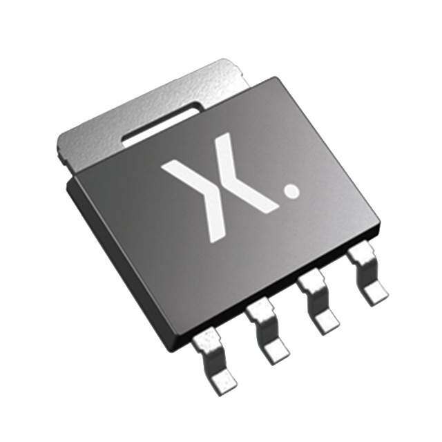
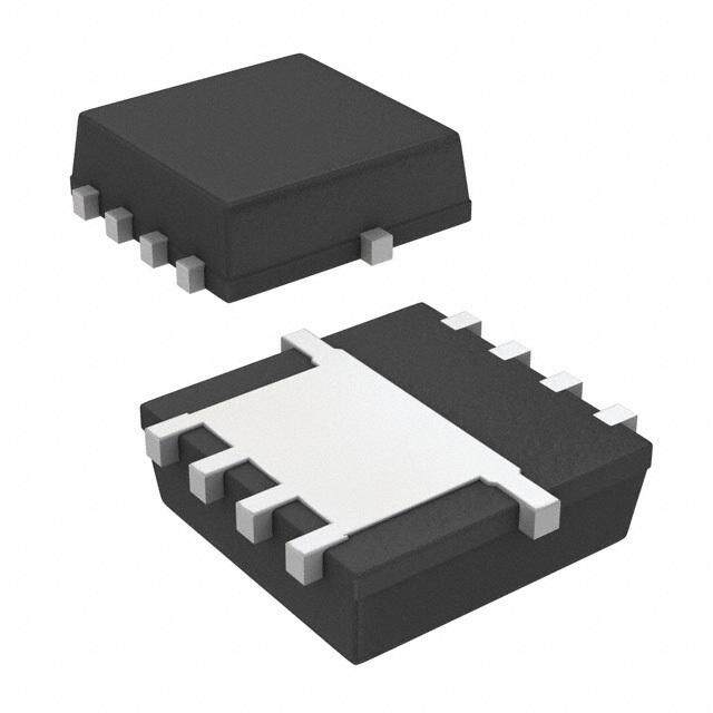
| 产品图片 |
|
| rohs | 符合RoHS无铅 / 符合限制有害物质指令(RoHS)规范要求 |
| 产品系列 | 晶体管,MOSFET,NXP Semiconductors PSMN8R5-60YS,115- |
| 数据手册 | |
| 产品型号 | PSMN8R5-60YS,115 |
| PCN组件/产地 | |
| Pd-PowerDissipation | 106 W |
| Pd-功率耗散 | 106 W |
| Qg-GateCharge | 39 nC |
| Qg-栅极电荷 | 39 nC |
| RdsOn-Drain-SourceResistance | 12.8 mOhms |
| RdsOn-漏源导通电阻 | 12.8 mOhms |
| Vds-Drain-SourceBreakdownVoltage | 60 V |
| Vds-漏源极击穿电压 | 60 V |
| Vgs-Gate-SourceBreakdownVoltage | +/- 20 V |
| Vgs-栅源极击穿电压 | 20 V |
| Vgsth-Gate-SourceThresholdVoltage | 4.6 V |
| Vgsth-栅源极阈值电压 | 4.6 V |
| 上升时间 | 13.7 ns |
| 下降时间 | 9.2 ns |
| 不同Id时的Vgs(th)(最大值) | 4V @ 1mA |
| 不同Vds时的输入电容(Ciss) | 2370pF @ 30V |
| 不同Vgs时的栅极电荷(Qg) | 39nC @ 10V |
| 不同 Id、Vgs时的 RdsOn(最大值) | 8 毫欧 @ 15A,10V |
| 产品目录页面 | |
| 产品种类 | MOSFET |
| 供应商器件封装 | LFPAK56, Power-SO8 |
| 其它名称 | 568-4969-1 |
| 典型关闭延迟时间 | 32.4 ns |
| 功率-最大值 | 106W |
| 包装 | 剪切带 (CT) |
| 商标 | NXP Semiconductors |
| 安装类型 | 表面贴装 |
| 安装风格 | SMD/SMT |
| 封装 | Reel |
| 封装/外壳 | SC-100,SOT-669,4-LFPAK |
| 封装/箱体 | LFPAK-4 |
| 工厂包装数量 | 1500 |
| 晶体管极性 | N-Channel |
| 最大工作温度 | + 175 C |
| 最小工作温度 | - 55 C |
| 标准包装 | 1 |
| 漏源极电压(Vdss) | 60V |
| 电流-连续漏极(Id)(25°C时) | 76A (Tc) |
| 通道模式 | Enhancement |
| 配置 | Single Triple Source |


PDF Datasheet 数据手册内容提取
PSMN8R5-60YS N-channel LFPAK 60 V, 8 mΩ standard level MOSFET 22 July 2015 Product data sheet 1. General description Standard level N-channel MOSFET in LFPAK package qualified to 175 °C. This product is designed and qualified for use in a wide range of industrial, communications and domestic equipment. 2. Features and benefits • Advanced TrenchMOS provides low RDSon and low gate charge • High efficiency gains in switching power converters • Improved mechanical and thermal characteristics • LFPAK provides maximum power density in a Power SO8 package 3. Applications • DC-to-DC converters • Lithium-ion battery protection • Load switching • Motor control • Server power supplies 4. Quick reference data Table 1. Quick reference data Symbol Parameter Conditions Min Typ Max Unit V drain-source voltage T ≥ 25 °C; T ≤ 175 °C - - 60 V DS j j I drain current T = 25 °C; V = 10 V; Fig. 2 - - 76 A D mb GS P total power dissipation T = 25 °C; Fig. 1 - - 106 W tot mb T junction temperature -55 - 175 °C j Static characteristics R drain-source on-state V = 10 V; I = 15 A; T = 100 °C; - - 12.8 mΩ DSon GS D j resistance Fig. 12 V = 10 V; I = 15 A; T = 25 °C; - 5.6 8 mΩ GS D j Fig. 13 Dynamic characteristics Q gate-drain charge V = 10 V; I = 60 A; V = 30 V; - 7.7 - nC GD GS D DS Fig. 15; Fig. 14
Nexperia PSMN8R5-60YS N-channel LFPAK 60 V, 8 mΩ standard level MOSFET Symbol Parameter Conditions Min Typ Max Unit Q total gate charge V = 10 V; I = 60 A; V = 30 V; - 39 - nC G(tot) GS D DS Fig. 14; Fig. 15 Avalanche ruggedness E non-repetitive drain- V = 10 V; T = 25 °C; I = 76 A; - - 97 mJ DS(AL)S GS j(init) D source avalanche V ≤ 60 V; R = 50 Ω; unclamped sup GS energy 5. Pinning information Table 2. Pinning information Pin Symbol Description Simplified outline Graphic symbol 1 S source mb D 2 S source G 3 S source 4 G gate mbb076 S 1 2 3 4 mb D mounting base; connected to LFPAK56; Power- drain SO8 (SOT669) 6. Ordering information Table 3. Ordering information Type number Package Name Description Version PSMN8R5-60YS LFPAK56; Plastic single-ended surface-mounted package SOT669 Power-SO8 (LFPAK56; Power-SO8); 4 leads 7. Marking Table 4. Marking codes Type number Marking code PSMN8R5-60YS 8R560 8. Limiting values Table 5. Limiting values In accordance with the Absolute Maximum Rating System (IEC 60134). Symbol Parameter Conditions Min Max Unit V drain-source voltage T ≥ 25 °C; T ≤ 175 °C - 60 V DS j j V drain-gate voltage T ≥ 25 °C; T ≤ 175 °C; R = 20 kΩ - 60 V DGR j j GS PSMN8R5-60YS All information provided in this document is subject to legal disclaimers. © Nexperia B.V. 2017. All rights reserved Product data sheet 22 July 2015 2 / 14
Nexperia PSMN8R5-60YS N-channel LFPAK 60 V, 8 mΩ standard level MOSFET Symbol Parameter Conditions Min Max Unit V gate-source voltage -20 20 V GS P total power dissipation T = 25 °C; Fig. 1 - 106 W tot mb I drain current V = 10 V; T = 100 °C; Fig. 2 - 54 A D GS mb V = 10 V; T = 25 °C; Fig. 2 - 76 A GS mb I peak drain current pulsed; t ≤ 10 µs; T = 25 °C; Fig. 3 - 303 A DM p mb T storage temperature -55 175 °C stg T junction temperature -55 175 °C j T peak soldering temperature - 260 °C sld(M) Source-drain diode I source current T = 25 °C - 76 A S mb I peak source current pulsed; t ≤ 10 µs; T = 25 °C - 303 A SM p mb Avalanche ruggedness E non-repetitive drain-source V = 10 V; T = 25 °C; I = 76 A; - 97 mJ DS(AL)S GS j(init) D avalanche energy V ≤ 60 V; R = 50 Ω; unclamped sup GS 03aa16 120 Pder (%) 80 40 0 0 50 100 150 200 Tmb(°C) Fig. 1. Normalized total power dissipation as a function of mounting base temperature PSMN8R5-60YS All information provided in this document is subject to legal disclaimers. © Nexperia B.V. 2017. All rights reserved Product data sheet 22 July 2015 3 / 14
Nexperia PSMN8R5-60YS N-channel LFPAK 60 V, 8 mΩ standard level MOSFET 003aad791 100 ID (A) 80 60 40 20 0 0 50 100 150 200 Tmb(°C) Fig. 2. Continuous drain current as a function of mounting base temperature 103 003aad792 ID (A) LimitRDSon=VDS/ID 102 tp=10µs 100µs 10 DC 1 1ms 10ms 100ms 10-1 10-1 1 10 102 103 VDS(V) Fig. 3. Safe operating area; continuous and peak drain currents as a function of drain-source voltage 9. Thermal characteristics Table 6. Thermal characteristics Symbol Parameter Conditions Min Typ Max Unit R thermal resistance Fig. 4 - 0.63 1.42 K/W th(j-mb) from junction to mounting base PSMN8R5-60YS All information provided in this document is subject to legal disclaimers. © Nexperia B.V. 2017. All rights reserved Product data sheet 22 July 2015 4 / 14
Nexperia PSMN8R5-60YS N-channel LFPAK 60 V, 8 mΩ standard level MOSFET 003aad834 1 Zth(j-mb) d=0.5 (K/W) 0.2 10-1 0.1 0.05 10-2 0.02 P δ= Ttp singleshot tp t T 10-3 10-6 10-5 10-4 10-3 10-2 10-1 tp(s) 1 Fig. 4. Transient thermal impedance from junction to mounting base as a function of pulse duration; typical values 10. Characteristics Table 7. Characteristics Symbol Parameter Conditions Min Typ Max Unit Static characteristics V drain-source I = 250 µA; V = 0 V; T = -55 °C 54 - - V (BR)DSS D GS j breakdown voltage I = 250 µA; V = 0 V; T = 25 °C 60 - - V D GS j V gate-source threshold I = 1 mA; V = V ; T = 25 °C; 2 3 3.8 V GS(th) D DS GS j voltage Fig. 10; Fig. 11 V gate-source threshold I = 1 mA; V = V ; T = -55 °C; - - 4.3 V GSth D DS GS j voltage Fig. 11 I = 1 mA; V = V ; T = 175 °C; 0.95 - - V D DS GS j Fig. 11 I drain leakage current V = 60 V; V = 0 V; T = 25 °C - 0.03 2 µA DSS DS GS j V = 60 V; V = 0 V; T = 125 °C - - 50 µA DS GS j I gate leakage current V = 20 V; V = 0 V; T = 25 °C - 2 100 nA GSS GS DS j V = -20 V; V = 0 V; T = 25 °C - 2 100 nA GS DS j R drain-source on-state V = 10 V; I = 15 A; T = 175 °C; - 12 18.4 mΩ DSon GS D j resistance Fig. 12 V = 10 V; I = 15 A; T = 100 °C; - - 12.8 mΩ GS D j Fig. 12 V = 10 V; I = 15 A; T = 25 °C; - 5.6 8 mΩ GS D j Fig. 13 R gate resistance f = 1 MHz - 0.61 - Ω G PSMN8R5-60YS All information provided in this document is subject to legal disclaimers. © Nexperia B.V. 2017. All rights reserved Product data sheet 22 July 2015 5 / 14
Nexperia PSMN8R5-60YS N-channel LFPAK 60 V, 8 mΩ standard level MOSFET Symbol Parameter Conditions Min Typ Max Unit Dynamic characteristics Q total gate charge I = 60 A; V = 30 V; V = 10 V; - 39 - nC G(tot) D DS GS Fig. 14; Fig. 15 I = 0 A; V = 0 V; V = 10 V - 33 - nC D DS GS Q gate-source charge I = 60 A; V = 30 V; V = 10 V; - 13.3 - nC GS D DS GS Fig. 15; Fig. 14 Q pre-threshold gate- I = 60 A; V = 30 V; V = 10 V; - 7 - nC GS(th) D DS GS source charge Fig. 14 Q post-threshold gate- - 6.2 - nC GS(th-pl) source charge Q gate-drain charge I = 60 A; V = 30 V; V = 10 V; - 7.7 - nC GD D DS GS Fig. 15; Fig. 14 V gate-source plateau V = 30 V; Fig. 14; Fig. 15 - 5.2 - V GS(pl) DS voltage C input capacitance V = 30 V; V = 0 V; f = 1 MHz; - 2370 - pF iss DS GS T = 25 °C; Fig. 16 C output capacitance j - 307 - pF oss C reverse transfer - 172 - pF rss capacitance t turn-on delay time V = 30 V; R = 0.5 Ω; V = 10 V; - 18.4 - ns d(on) DS L GS R = 4.7 Ω t rise time G(ext) - 13.7 - ns r t turn-off delay time - 32.4 - ns d(off) t fall time - 9.2 - ns f Source-drain diode V source-drain voltage I = 15 A; V = 0 V; T = 25 °C; Fig. 17 - 0.8 1.2 V SD S GS j t reverse recovery time I = 20 A; dI /dt = -100 A/µs; V = 0 V; - 43.3 - ns rr S S GS V = 30 V Q recovered charge DS - 61.4 - nC r PSMN8R5-60YS All information provided in this document is subject to legal disclaimers. © Nexperia B.V. 2017. All rights reserved Product data sheet 22 July 2015 6 / 14
Nexperia PSMN8R5-60YS N-channel LFPAK 60 V, 8 mΩ standard level MOSFET 60 003aad794 4000 003aad801 gfs C Ciss (pF) (S) 3000 40 Crss 2000 20 1000 0 0 0 20 40 60 80 0 3 6 9 12 ID(A) VGS(V) Fig. 5. Forward transconductance as a function of Fig. 6. Input and reverse transfer capacitances as a drain current; typical values function of gate-source voltage, typical values 003aad797 003aad795 40 80 RDSon ID 10 7 6 5.5 (A) (mΩ) 30 60 5 20 40 VGS(V)=4.5 10 20 0 0 4 8 12 16 20 0 0.5 1 1.5 2 VGS(V) VDS(V) Fig. 7. Drain-source on-state resistance as a function Fig. 8. Output characteristics: drain current as a of gate-source voltage; typical values function of drain-source voltage; typical values PSMN8R5-60YS All information provided in this document is subject to legal disclaimers. © Nexperia B.V. 2017. All rights reserved Product data sheet 22 July 2015 7 / 14
Nexperia PSMN8R5-60YS N-channel LFPAK 60 V, 8 mΩ standard level MOSFET 80 003aad796 10-1 aaa-019191 IIDD ID ((AA)) (A) 10-2 60 MMiinn TTyypp MMaaxx 10-3 40 10-4 20 Tj=175°C Tj=25°C 10-5 0 10-6 0 2 4 6 0 1 2 3 4 5 VGS(V) VGS (V) T = 25 °C; V = 5V Fig. 9. Transfer characteristics: drain current as a j DS function of gate-source voltage; typical values Fig. 10. Sub-threshold drain current as a function of gate-source voltage aaa-019190 003aad696 5 2.4 VVGGSS((tthh)) a ((VV)) 2 4 MMaaxx 1.6 3 TTyypp 1.2 2 MMiinn 0.8 1 0.4 0 0 -60 -30 0 30 60 90 120 150 180 -60 0 60 120 180 Tj (°C) Tj(°C) I = 1 mA ; V = V D DS GS Fig. 12. Normalized drain-source on-state resistance Fig. 11. Gate-source threshold voltage as a function of factor as a function of junction temperature. junction temperature PSMN8R5-60YS All information provided in this document is subject to legal disclaimers. © Nexperia B.V. 2017. All rights reserved Product data sheet 22 July 2015 8 / 14
Nexperia PSMN8R5-60YS N-channel LFPAK 60 V, 8 mΩ standard level MOSFET 003aad798 25 RDSon VGS(V)=5 5.5 VDS (mΩ) ID 20 VGS(pl) 15 VGS(th) VGS 6 QGS2 10 7 QGS1 8 QGS QGD 10 QG(tot) 003aaa508 5 Fig. 14. Gate charge waveform definitions 0 20 40 60 80 ID(A) Fig. 13. Drain-source on-state resistance as a function of drain current; typical values 10 003aad799 104 003aad800 VGS (V) 12V C (pF) 8 VDS=30V 48V Ciss 6 103 4 Coss 2 Crss 0 102 0 20 40 60 10-1 1 10 102 QG(nC) VDS(V) Fig. 15. Gate-source voltage as a function of gate Fig. 16. Input, output and reverse transfer capacitances charge; typical values as a function of drain-source voltage; typical values PSMN8R5-60YS All information provided in this document is subject to legal disclaimers. © Nexperia B.V. 2017. All rights reserved Product data sheet 22 July 2015 9 / 14
Nexperia PSMN8R5-60YS N-channel LFPAK 60 V, 8 mΩ standard level MOSFET 003aad802 80 IS (A) 60 40 20 Tj=175°C Tj=25°C 0 0 0.4 0.8 1.2 VSD(V) Fig. 17. Source (diode forward) current as a function of source-drain (diode forward) voltage; typical values PSMN8R5-60YS All information provided in this document is subject to legal disclaimers. © Nexperia B.V. 2017. All rights reserved Product data sheet 22 July 2015 10 / 14
Nexperia PSMN8R5-60YS N-channel LFPAK 60 V, 8 mΩ standard level MOSFET 11. Package outline Plastic single-ended surface-mounted package (LFPAK56; Power-SO8); 4 leads SOT669 E A A2 C b2 c2 E1 L1 b3 mounting base b4 D1 H D L2 1 2 3 4 X e b w A c 1/2 e A (A3) A1 C q L detail X y C 0 5 mm θ scale 8° 0° Dimensions (mm are the original dimensions) Unit(1) A A1 A2 A3 b b2 b3 b4 c c2 D(1) D1(1) E(1) E1(1) e H L L1 L2 w y max 1.20 0.15 1.10 0.50 4.41 2.2 0.9 0.25 0.30 4.10 4.20 5.0 3.3 6.2 0.85 1.3 1.3 mm nom 0.25 1.27 0.25 0.1 min 1.01 0.00 0.95 0.35 3.62 2.0 0.7 0.19 0.24 3.80 4.8 3.1 5.8 0.40 0.8 0.8 Note 1. Plastic or metal protrusions of 0.15 mm maximum per side are not included. sot669_po Outline References European Issue date version IEC JEDEC JEITA projection 11-03-25 SOT669 MO-235 13-02-27 Fig. 18. Package outline LFPAK56; Power-SO8 (SOT669) PSMN8R5-60YS All information provided in this document is subject to legal disclaimers. © Nexperia B.V. 2017. All rights reserved Product data sheet 22 July 2015 11 / 14
Nexperia PSMN8R5-60YS N-channel LFPAK 60 V, 8 mΩ standard level MOSFET In no event shall Nexperia be liable for any indirect, incidental, punitive, special or consequential damages (including - without limitation - 12. Legal information lost profits, lost savings, business interruption, costs related to the removal or replacement of any products or rework charges) whether or not such damages are based on tort (including negligence), warranty, breach of contract or any other legal theory. 12.1 Data sheet status Notwithstanding any damages that customer might incur for any reason whatsoever, Nexperia’s aggregate and cumulative liability towards customer for the products described herein shall be limited in accordance Document Product Definition with the Terms and conditions of commercial sale of Nexperia. status [1][2] status [3] Objective Development This document contains data from Right to make changes — Nexperia reserves the right to [short] data the objective specification for product make changes to information published in this document, including without sheet development. limitation specifications and product descriptions, at any time and without Preliminary Qualification This document contains data from the notice. This document supersedes and replaces all information supplied prior [short] data preliminary specification. to the publication hereof. sheet Suitability for use — Nexperia products are not designed, Product Production This document contains the product authorized or warranted to be suitable for use in life support, life-critical or [short] data specification. safety-critical systems or equipment, nor in applications where failure or sheet malfunction of a Nexperia product can reasonably be expected to result in personal injury, death or severe property or environmental [1] Please consult the most recently issued document before initiating or damage. Nexperia and its suppliers accept no liability for completing a design. inclusion and/or use of Nexperia products in such equipment or [2] The term 'short data sheet' is explained in section "Definitions". applications and therefore such inclusion and/or use is at the customer’s own [3] The product status of device(s) described in this document may have risk. changed since this document was published and may differ in case of multiple devices. The latest product status information is available on Quick reference data — The Quick reference data is an extract of the the Internet at URL http://www.nexperia.com. product data given in the Limiting values and Characteristics sections of this document, and as such is not complete, exhaustive or legally binding. Applications — Applications that are described herein for any of these 12.2 Definitions products are for illustrative purposes only. Nexperia makes no representation or warranty that such applications will be suitable for the Preview — The document is a preview version only. The document is still specified use without further testing or modification. subject to formal approval, which may result in modifications or additions. Nexperia does not give any representations or warranties as to Customers are responsible for the design and operation of their the accuracy or completeness of information included herein and shall have applications and products using Nexperia products, and Nexperia no liability for the consequences of use of such information. accepts no liability for any assistance with applications or customer product design. It is customer’s sole responsibility to determine Draft — The document is a draft version only. The content is still under whether the Nexperia product is suitable and fit for the internal review and subject to formal approval, which may result in customer’s applications and products planned, as well as for the planned modifications or additions. Nexperia does not give any application and use of customer’s third party customer(s). Customers should representations or warranties as to the accuracy or completeness of provide appropriate design and operating safeguards to minimize the risks information included herein and shall have no liability for the consequences associated with their applications and products. of use of such information. Nexperia does not accept any liability related to any default, Short data sheet — A short data sheet is an extract from a full data sheet damage, costs or problem which is based on any weakness or default with the same product type number(s) and title. A short data sheet is in the customer’s applications or products, or the application or use by intended for quick reference only and should not be relied upon to contain customer’s third party customer(s). Customer is responsible for doing all detailed and full information. For detailed and full information see the necessary testing for the customer’s applications and products using Nexperia relevant full data sheet, which is available on request via the local Nexperia products in order to avoid a default of the applications sales office. In case of any inconsistency or conflict with the and the products or of the application or use by customer’s third party short data sheet, the full data sheet shall prevail. customer(s). Nexperia does not accept any liability in this respect. Product specification — The information and data provided in a Product Limiting values — Stress above one or more limiting values (as defined in data sheet shall define the specification of the product as agreed between the Absolute Maximum Ratings System of IEC 60134) will cause permanent Nexperia and its customer, unless Nexperia and damage to the device. Limiting values are stress ratings only and (proper) customer have explicitly agreed otherwise in writing. In no event however, operation of the device at these or any other conditions above those shall an agreement be valid in which the Nexperia product given in the Recommended operating conditions section (if present) or the is deemed to offer functions and qualities beyond those described in the Characteristics sections of this document is not warranted. Constant or Product data sheet. repeated exposure to limiting values will permanently and irreversibly affect the quality and reliability of the device. Terms and conditions of commercial sale — Nexperia 12.3 Disclaimers products are sold subject to the general terms and conditions of commercial sale, as published at http://www.nexperia.com/profile/terms, unless otherwise Limited warranty and liability — Information in this document is believed agreed in a valid written individual agreement. In case an individual to be accurate and reliable. However, Nexperia does not give agreement is concluded only the terms and conditions of the respective any representations or warranties, expressed or implied, as to the accuracy agreement shall apply. Nexperia hereby expressly objects to or completeness of such information and shall have no liability for the applying the customer’s general terms and conditions with regard to the consequences of use of such information. Nexperia takes no purchase of Nexperia products by customer. responsibility for the content in this document if provided by an information source outside of Nexperia. No offer to sell or license — Nothing in this document may be interpreted or construed as an offer to sell products that is open for acceptance or the PSMN8R5-60YS All information provided in this document is subject to legal disclaimers. © Nexperia B.V. 2017. All rights reserved Product data sheet 22 July 2015 12 / 14
Nexperia PSMN8R5-60YS N-channel LFPAK 60 V, 8 mΩ standard level MOSFET grant, conveyance or implication of any license under any copyrights, patents or other industrial or intellectual property rights. Export control — This document as well as the item(s) described herein may be subject to export control regulations. Export might require a prior authorization from competent authorities. Non-automotive qualified products — Unless this data sheet expressly states that this specific Nexperia product is automotive qualified, the product is not suitable for automotive use. It is neither qualified nor tested in accordance with automotive testing or application requirements. Nexperia accepts no liability for inclusion and/or use of non- automotive qualified products in automotive equipment or applications. In the event that customer uses the product for design-in and use in automotive applications to automotive specifications and standards, customer (a) shall use the product without Nexperia’s warranty of the product for such automotive applications, use and specifications, and (b) whenever customer uses the product for automotive applications beyond Nexperia’s specifications such use shall be solely at customer’s own risk, and (c) customer fully indemnifies Nexperia for any liability, damages or failed product claims resulting from customer design and use of the product for automotive applications beyond Nexperia’s standard warranty and Nexperia’s product specifications. Translations — A non-English (translated) version of a document is for reference only. The English version shall prevail in case of any discrepancy between the translated and English versions. 12.4 Trademarks Notice: All referenced brands, product names, service names and trademarks are the property of their respective owners. PSMN8R5-60YS All information provided in this document is subject to legal disclaimers. © Nexperia B.V. 2017. All rights reserved Product data sheet 22 July 2015 13 / 14
Nexperia PSMN8R5-60YS N-channel LFPAK 60 V, 8 mΩ standard level MOSFET 13. Contents 1 General description ...............................................1 2 Features and benefits ............................................1 3 Applications ...........................................................1 4 Quick reference data .............................................1 5 Pinning information ...............................................2 6 Ordering information .............................................2 7 Marking ...................................................................2 8 Limiting values .......................................................2 9 Thermal characteristics .........................................4 10 Characteristics .......................................................5 11 Package outline ...................................................11 12 Legal information .................................................12 12.1 Data sheet status ...............................................12 12.2 Definitions ...........................................................12 12.3 Disclaimers .........................................................12 12.4 Trademarks ........................................................13 © Nexperia B.V. 2017. All rights reserved For more information, please visit: http://www.nexperia.com For sales office addresses, please send an email to: salesaddresses@nexperia.com Date of release: 22 July 2015 PSMN8R5-60YS All information provided in this document is subject to legal disclaimers. © Nexperia B.V. 2017. All rights reserved Product data sheet 22 July 2015 14 / 14