ICGOO在线商城 > 分立半导体产品 > 晶体管 - FET,MOSFET - 单 > FDB3502
 Datasheet下载
- 型号: FDB3502
- 制造商: Fairchild Semiconductor
- 库位|库存: xxxx|xxxx
- 要求:
| 数量阶梯 | 香港交货 | 国内含税 |
| +xxxx | $xxxx | ¥xxxx |
查看当月历史价格
查看今年历史价格
FDB3502产品简介:
ICGOO电子元器件商城为您提供FDB3502由Fairchild Semiconductor设计生产,在icgoo商城现货销售,并且可以通过原厂、代理商等渠道进行代购。 FDB3502价格参考¥6.57-¥6.57。Fairchild SemiconductorFDB3502封装/规格:晶体管 - FET,MOSFET - 单, 表面贴装 N 沟道 75V 6A(Ta),14A(Tc) 3.1W(Ta),41W(Tc) TO-263AB。您可以下载FDB3502参考资料、Datasheet数据手册功能说明书,资料中有FDB3502 详细功能的应用电路图电压和使用方法及教程。
FDB3502是安森美半导体(ON Semiconductor)生产的一款N沟道增强型MOSFET,属于功率MOSFET器件,常用于需要高效开关和功率控制的电路中。该器件具有低导通电阻、高开关速度和良好热性能的特点,适合多种电源管理和功率转换应用。

其典型应用场景包括:

1. 电源管理:如DC-DC转换器、同步整流器等,用于提高能量转换效率。
2. 电机驱动:适用于小型电机或步进电机的驱动控制电路。
3. 负载开关:作为电子开关控制电源对负载的供给,例如在电池供电设备中控制不同模块的供电。
4. LED照明驱动:用于调光或恒流控制电路中,实现高效的LED驱动方案。
5. 汽车电子:如车载充电系统、车身控制模块等对可靠性要求较高的场景。

由于其封装小巧、性能稳定,FDB3502也广泛应用于便携式电子产品、工业控制系统以及消费类电子设备中。
| 参数 | 数值 |
| 产品目录 | |
| ChannelMode | Enhancement |
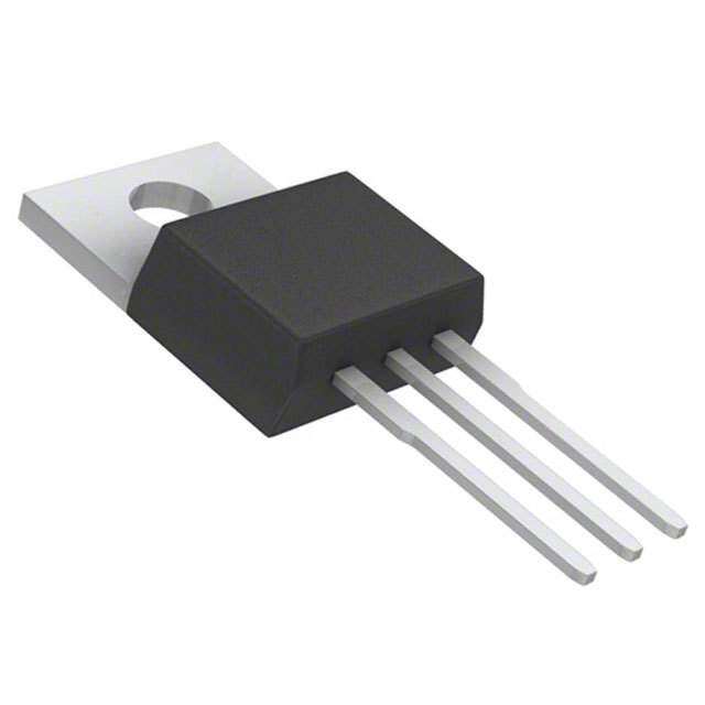
| 描述 | MOSFET N-CH 75V 6A TO-263ABMOSFET 75V N-Channel PowerTrench |
| 产品分类 | FET - 单分离式半导体 |
| FET功能 | 标准 |
| FET类型 | MOSFET N 通道,金属氧化物 |
| Id-ContinuousDrainCurrent | 6 A |
| Id-连续漏极电流 | 6 A |
| 品牌 | Fairchild Semiconductor |
| 产品手册 | |
| 产品图片 |
|
| rohs | 符合RoHS无铅 / 符合限制有害物质指令(RoHS)规范要求 |
| 产品系列 | 晶体管,MOSFET,Fairchild Semiconductor FDB3502PowerTrench® |
| 数据手册 | |
| 产品型号 | FDB3502 |
| PCN封装 | |
| Pd-PowerDissipation | 3.1 W |
| Pd-功率耗散 | 3.1 W |
| RdsOn-Drain-SourceResistance | 47 mOhms |
| RdsOn-漏源导通电阻 | 47 mOhms |
| Vds-Drain-SourceBreakdownVoltage | 75 V |
| Vds-漏源极击穿电压 | 75 V |
| Vgs-Gate-SourceBreakdownVoltage | +/- 20 V |
| Vgs-栅源极击穿电压 | 20 V |
| 上升时间 | 3 ns |
| 下降时间 | 3 ns |
| 不同Id时的Vgs(th)(最大值) | 4.5V @ 250µA |
| 不同Vds时的输入电容(Ciss) | 815pF @ 40V |
| 不同Vgs时的栅极电荷(Qg) | 15nC @ 10V |
| 不同 Id、Vgs时的 RdsOn(最大值) | 47 毫欧 @ 6A,10V |
| 产品目录页面 | |
| 产品种类 | MOSFET |
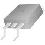
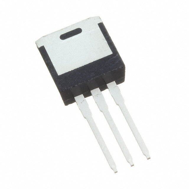
| 供应商器件封装 | TO-263AB |
| 其它名称 | FDB3502TR |
| 典型关闭延迟时间 | 13 ns |
| 功率-最大值 | 3.1W |
| 包装 | 带卷 (TR) |
| 单位重量 | 1.312 g |
| 商标 | Fairchild Semiconductor |
| 安装类型 | 表面贴装 |
| 安装风格 | SMD/SMT |
| 封装 | Reel |
| 封装/外壳 | TO-263-3,D²Pak(2 引线+接片),TO-263AB |
| 封装/箱体 | D2PAK-2 |
| 工厂包装数量 | 800 |
| 晶体管极性 | N-Channel |
| 最大工作温度 | + 150 C |
| 最小工作温度 | - 55 C |
| 标准包装 | 800 |
| 漏源极电压(Vdss) | 75V |
| 电流-连续漏极(Id)(25°C时) | 6A (Ta), 14A (Tc) |
| 系列 | FDB3502 |
| 通道模式 | Enhancement |
| 配置 | Single |


.jpg)


- 商务部:美国ITC正式对集成电路等产品启动337调查
- 曝三星4nm工艺存在良率问题 高通将骁龙8 Gen1或转产台积电
- 太阳诱电将投资9.5亿元在常州建新厂生产MLCC 预计2023年完工
- 英特尔发布欧洲新工厂建设计划 深化IDM 2.0 战略
- 台积电先进制程称霸业界 有大客户加持明年业绩稳了
- 达到5530亿美元!SIA预计今年全球半导体销售额将创下新高
- 英特尔拟将自动驾驶子公司Mobileye上市 估值或超500亿美元
- 三星加码芯片和SET,合并消费电子和移动部门,撤换高东真等 CEO
- 三星电子宣布重大人事变动 还合并消费电子和移动部门
- 海关总署:前11个月进口集成电路产品价值2.52万亿元 增长14.8%


PDF Datasheet 数据手册内容提取
Is Now Part of To learn more about ON Semiconductor, please visit our website at www.onsemi.com Please note: As part of the Fairchild Semiconductor integration, some of the Fairchild orderable part numbers will need to change in order to meet ON Semiconductor’s system requirements. Since the ON Semiconductor product management systems do not have the ability to manage part nomenclature that utilizes an underscore (_), the underscore (_) in the Fairchild part numbers will be changed to a dash (-). This document may contain device numbers with an underscore (_). Please check the ON Semiconductor website to verify the updated device numbers. The most current and up-to-date ordering information can be found at www.onsemi.com. Please email any questions regarding the system integration to Fairchild_questions@onsemi.com. ON Semiconductor and the ON Semiconductor logo are trademarks of Semiconductor Components Industries, LLC dba ON Semiconductor or its subsidiaries in the United States and/or other countries. ON Semiconductor owns the rights to a number of patents, trademarks, copyrights, trade secrets, and other intellectual property. A listing of ON Semiconductor’s product/patent coverage may be accessed at www.onsemi.com/site/pdf/Patent-Marking.pdf. ON Semiconductor reserves the right to make changes without further notice to any products herein. ON Semiconductor makes no warranty, representation or guarantee regarding the suitability of its products for any particular purpose, nor does ON Semiconductor assume any liability arising out of the application or use of any product or circuit, and specifically disclaims any and all liability, including without limitation special, consequential or incidental damages. Buyer is responsible for its products and applications using ON Semiconductor products, including compliance with all laws, regulations and safety requirements or standards, regardless of any support or applications information provided by ON Semiconductor. “Typical” parameters which may be provided in ON Semiconductor data sheets and/or specifications can and do vary in different applications and actual performance may vary over time. All operating parameters, including “Typicals” must be validated for each customer application by customer’s technical experts. ON Semiconductor does not convey any license under its patent rights nor the rights of others. ON Semiconductor products are not designed, intended, or authorized for use as a critical component in life support systems or any FDA Class 3 medical devices or medical devices with a same or similar classification in a foreign jurisdiction or any devices intended for implantation in the human body. Should Buyer purchase or use ON Semiconductor products for any such unintended or unauthorized application, Buyer shall indemnify and hold ON Semiconductor and its officers, employees, subsidiaries, affiliates, and distributors harmless against all claims, costs, damages, and expenses, and reasonable attorney fees arising out of, directly or indirectly, any claim of personal injury or death associated with such unintended or unauthorized use, even if such claim alleges that ON Semiconductor was negligent regarding the design or manufacture of the part. ON Semiconductor is an Equal Opportunity/Affirmative Action Employer. This literature is subject to all applicable copyright laws and is not for resale in any manner.
F D B 3 5 May 2008 0 2 FDB3502 N - tm C ® N-Channel Power Trench MOSFET h a 75V, 14A, 47mΩ n n e Features General Description l P (cid:132) Max rDS(on) = 47mΩ at VGS = 10V, ID = 6A This N-Channel MOSFET is produced using Fairchild o Semiconductor‘s advanced Power Trench® process that has w (cid:132) 100% UIL Tested been especially tailored to minimize the on-state resistance and e r (cid:132) RoHS Compliant yet maintain superior switching performance. T r e n Application c h ® (cid:132) Synchronous rectifier M O S F E T D D G G S TO-263AB FDB Series S MOSFET Maximum Ratings TC = 25°C unless otherwise noted Symbol Parameter Ratings Units V Drain to Source Voltage 75 V DS V Gate to Source Voltage ±20 V GS Drain Current -Continuous (Package limited) T = 25°C 14 C -Continuous (Silicon limited) T = 25°C 22 I C A D -Continuous T = 25°C (Note 1a) 6 A -Pulsed 40 E Single Pulse Avalanche Energy (Note 3) 54 mJ AS Power Dissipation T = 25°C 41 P C W D Power Dissipation T = 25°C (Note 1a) 3.1 A T , T Operating and Storage Junction Temperature Range -55 to +150 °C J STG Thermal Characteristics R Thermal Resistance, Junction to Case 3 θJC °C/W R Thermal Resistance, Junction to Ambient (Note 1a) 40 θJA Package Marking and Ordering Information Device Marking Device Package Reel Size Tape Width Quantity FDB3502 FDB3502 TO-263AB 330 mm 24 mm 800 units ©2008 Fairchild Semiconductor Corporation 1 www.fairchildsemi.com FDB3502 Rev.C2
F D Electrical Characteristics B T = 25°C unless otherwise noted J 3 5 Symbol Parameter Test Conditions Min Typ Max Units 0 2 Off Characteristics N - BVDSS Drain to Source Breakdown Voltage ID = 250µA, VGS = 0V 75 V C h ∆BV Breakdown Voltage Temperature DSS I = 250µA, referenced to 25°C 70 mV/°C a ∆TJ Coefficient D n n I Zero Gate Voltage Drain Current V = 0V, V = 60V, 1 µA DSS GS DS e IGSS Gate to Source Leakage Current VGS = ±20V, VDS = 0V ±100 nA l P o On Characteristics w e VGS(th) Gate to Source Threshold Voltage VGS = VDS, ID = 250µA 2.5 3.8 4.5 V r ∆V Gate to Source Threshold Voltage T ∆TGJS(th) Temperature Coefficient ID = 250µA, referenced to 25°C -10 mV/°C re n rDS(on) Static Drain to Source On Resistance VVGS == 1100VV,, IID == 66AA , T = 125°C 3673 4870 mΩ ch GS D J ® gFS Forward Transconductance VDD = 10V, ID = 6A 13 S M O Dynamic Characteristics S C Input Capacitance 615 815 pF F iss V = 40V, V = 0V, E Coss Output Capacitance f =D S1MHz GS 75 105 pF T C Reverse Transfer Capacitance 35 40 pF rss R Gate Resistance f = 1MHz 1.5 Ω g Switching Characteristics t Turn-On Delay Time 9 17 ns d(on) tr Rise Time VDD = 40V, ID = 6A, 3 10 ns td(off) Turn-Off Delay Time VGS = 10V, RGEN = 6Ω 13 22 ns t Fall Time 3 10 ns f Q Total Gate Charge at 10V 11 15 nC g V = 40V Q Gate to Source Charge DD 4 nC gs I = 6A D Q Gate to Drain “Miller” Charge 3 nC gd Drain-Source Diode Characteristics V = 0V, I = 2.6A (Note 2) 0.78 1.2 V Source to Drain Diode Forward Voltage GS S V SD V = 0V, I = 6A (Note 2) 0.83 1.3 GS S t Reverse Recovery Time 25 41 ns rr I = 6A, di/dt = 100A/µs Q Reverse Recovery Charge F 17 32 nC rr Notes: 1: RθJA is the sum of the junction-to-case and case-to-ambient thermal resistance where the case thermal reference is defined as the solder mounting surface of the drain pins. RθJC is guaranteed by design while RθJA is determined by the user’s board design. a. 40°C/W when mounted on a 1 in2 pad of 2 oz copper b. 62.5°C/W when mounted on a minimum pad. 2: Pulse Test: Pulse Width < 300µs, Duty cycle < 2.0%. 3: Starting TJ = 25°C, L = 3mH, IAS = 6A, VDD = 75V, VGS = 10V. ©2008 Fairchild Semiconductor Corporation 2 www.fairchildsemi.com FDB3502 Rev.C2
F D Typical Characteristics B TJ = 25°C unless otherwise noted 3 5 0 40 3.0 2 RAIN CURRENT (A) 1223350505 VGSV =G S 9 =V 10V PDUULTSYE C DYUCRLEA T=I O0VV.N5GG %=SS M==8 0A78µXVVs NORMALIZED SOURCE ON-RESISTANCE 122...505 VGS = 6V VVGGSS == 97VV VGS = 8V N-Channel Pow , IDD 105 V = 6V AIN TO 1.0 PULSE DURATIONV =G 8S 0=µ s10V er T GS R DUTY CYCLE = 0.5%MAX r 0 D 0.5 e 0 1 2 3 4 5 0 5 10 15 20 25 30 35 40 n c VDS, DRAIN TO SO URCE VOLTAGE (V) ID, DRAIN CURR ENT(A) h ® Figure 1. On-Region Characteristics Figure 2. Normalized On-Resistance M vs Drain Current and Gate Voltage O S F 2.0 150 E TANCE 1.8 IVDG =S 6=A 10V ()mΩ120 PDUULTSYE C DYUCRLEA T=I O0.N5 %= M80AµXs T NORMALIZED O SOURCE ON-RESIS 1111....0246 rDRAIN TO ,DS(on)CE ON-RESISTANCE 6900 ID = 6A TJ = 125oC AIN T 0.8 SOUR 30 TJ = 25oC R D 0.6 0 -75 -50 -25 0 25 50 75 100 125 150 5 6 7 8 9 10 TJ, JUNCTION TEM PERATURE (oC) VGS, GATE TO SOURCE VOLTAGE (V) Figure 3. Normalized On- Resistance Figure 4. On-Resistance vs Gate to vs Junction Temperature Source Voltage 40 40 A) PULSE DURATION = 80µs T ( 10 VGS = 0V DUTY CYCLE = 0.5%MAX N T (A) 30 VDS = 7V URRE 1 TJ = 150oC EN N C TJ = 25oC RAIN CURR 20 TJ = 150oC TJ = 25oC ERSE DRAI 0.1 I, DD 10 TJ = -55oC I, REVS0.01 TJ = -55oC 0 0.001 2 4 6 8 10 0.0 0.2 0.4 0.6 0.8 1.0 1.2 VGS, GATE TO SOU RCE VOLTAGE (V) VSD, BODY DIODE FOR WARD VOLTAGE (V) Figure 5. Transfer Characteristics Figure 6. Source to Drain Diode Forward Voltage vs Source Current ©2008 Fairchild Semiconductor Corporation 3 www.fairchildsemi.com FDB3502 Rev.C2
F D Typical Characteristics B T = 25°C unless otherwise noted J 3 5 0 10 1000 2 GE(V) 8 ID = 6A VDD = 40V Ciss N-C A T h CE VOL 6 VDD = 30V VDD = 50V CE (pF) ann SOUR 4 CITAN 100 el P E TO CAPA Coss ow , GATS 2 fV =G S1 M= H0Vz Crss er T VG 0 10 re 0 2 4 6 8 10 12 0.1 1 10 100 n Qg, GATE CH ARGE(nC) VDS, DRAIN TO SOU RCE VOLTAGE (V) ch ® Figure 7. Gate Charge Characteristics Figure 8. Capacitance vs Drain M to Source Voltage O S 10 25 F E T NT(A) T (A) 20 E N RR TJ = 25oC RE 15 U R E C CU VGS = 10V H N Limited by Package AVALANC TJ = 125oC , IDRAID105 RθJC = 3oC/W , S A I 1 0 0.01 0.1 1 10 25 50 75 100 125 150 tAV, TIME IN AVA LANCHE(ms) TC, CASE TEMPERATURE (oC) Figure 9. Unclamped Inductive Figure 10. Maximum Continuous Drain Switching Capability Current vs Case Temperature 100 104 W) V = 10V A) ER ( GS RENT (10 100us T POW 103 SINGLE PULSE UR EN RθJC = 3oC/W N C TLIHMISIT AERDE BAY I Sr NSI TC = 25oC I, DRAID 1 STJIN =G MLAEX DPS RU(oALnST)EED 1ms EAK TRA 102 00.0.51 RTCθJ =C 2=5 3oCoC/W 11D00C0mmss , PP()PK 10 0.1 1 10 100 300 10-5 10-4 10-3 10-2 10-1 1 VDS, DRAIN to SOUR CE VOLTAGE (V) t, PULSE WIDT H (sec) Figure 11. Forward Bias Safe Figure 12. Single Pulse Maximum Operating Area Power Dissipation ©2008 Fairchild Semiconductor Corporation 4 www.fairchildsemi.com FDB3502 Rev.C2
F D Typical Characteristics B T = 25°C unless otherwise noted J 3 5 0 2 2 N 1 DUTY CYCLE-DESCENDING ORDER -C AL D = 0.5 ha ERMZJCθ 00..21 nn MALIZED TH MPEDANCE, 0.1 000...000521 PDM t1 el Pow ORI t2 e N SRIθNJCG =L E3 oPCU/WLSE NDPEOUATTKYE SFT:AJ C= TPODRM: xD Z =θ Jtc1 /xt 2RθJc + TC r Tre n 0.01 c 10-5 10-4 10-3 10-2 10-1 1 h ® t, RECTANGULAR PULSE DURATION (sec) M Figure 13. Transient Thermal Response Curve O S F 2 E 1 DUTY CYCLE-DESCENDING ORDER T D = 0.5 AL 0.2 M A 0.1 ERZJθ 0.1 0.05 LIZED TH EDANCE, 00..0021 PDM AP RMIM 0.01 SINGLE PULSE t1 NO R = 62.5oC/W t2 θJA NOTES: (Note 1b) DUTY FACTOR: D = t1/t2 PEAK TJ = PDM x ZθJA x RθJA + TA 0.001 10-4 10-3 10-2 10-1 1 10 100 1000 t, RECTANGULAR PULSE DURATION (sec) Figure 14. Transient Thermal Response Curve ©2008 Fairchild Semiconductor Corporation 5 www.fairchildsemi.com FDB3502 Rev.C2
F D B 3 5 0 2 N - C TRADEMARKS h a The following includes registered and unregistered trademarks and service marks, owned by Fairchild Semiconductor and/or its global n subsidianries, and is not intended to be an exhaustive list of all such trademarks. n e ACEx® FPS™ PDP-SPM™ The Power Franchise® l Build it Now™ F-PFS™ Power-SPM™ P CorePLUS™ FRFET® PowerTrench® o tm w CorePOWER™ Global Power ResourceSM Programmable Active Droop™ TinyBoost™ e CROSSVOLT™ Green FPS™ QFET® TinyBuck™ r CTL™ Green FPS™ e-Series™ QS™ TinyLogic® T r Current Transfer Logic™ GTO™ Quiet Series™ TINYOPTO™ e EcoSPARK® IntelliMAX™ RapidConfigure™ TinyPower™ n c EfficentMax™ ISOPLANAR™ Saving our world 1mW at a time™ TinyPWM™ h EZSWITCH™ * MegaBuck™ SmartMax™ TinyWire™ ® ™ MICROCOUPLER™ SMART START™ µSerDes™ M MicroFET™ SPM® O ® MicroPak™ STEALTH™ S Fairctmhild® MillerDrive™ SuperFET™ UHC® F E Fairchild Semiconductor® MotionMax™ SuperSOT™-3 Ultra FRFET™ T FACT Quiet Series™ Motion-SPM™ SuperSOT™-6 UniFET™ FACT® OPTOLOGIC® SuperSOT™-8 VCX™ FAST® OPTOPLANAR® SuperMOS™ VisualMax™ FastvCore™ ® ® FlashWriter® * tm * EZSWITCH™ and FlashWriter® are trademarks of System General Corporation, used under license by Fairchild Semiconductor. DISCLAIMER FAIRCHILD SEMICONDUCTOR RESERVES THE RIGHT TO MAKE CHANGES WITHOUT FURTHER NOTICE TO ANY PRODUCTS HEREIN TO IMPROVE RELIABILITY, FUNCTION, OR DESIGN. FAIRCHILD DOES NOT ASSUME ANY LIABILITY ARISING OUT OF THE APPLICATION OR USE OF ANY PRODUCT OR CIRCUIT DESCRIBED HEREIN; NEITHER DOES IT CONVEY ANY LICENSE UNDER ITS PATENT RIGHTS, NOR THE RIGHTS OF OTHERS. THESE SPECIFICATIONS DO NOT EXPAND THE TERMS OF FAIRCHILD’S WORLDWIDE TERMS AND CONDITIONS, SPECIFICALLY THE WARRANTY THEREIN, WHICH COVERS THESE PRODUCTS. LIFE SUPPORT POLICY FAIRCHILD’S PRODUCTS ARE NOT AUTHORIZED FOR USE AS CRITICAL COMPONENTS IN LIFE SUPPORT DEVICES OR SYSTEMS WITHOUT THE EXPRESS WRITTEN APPROVAL OF FAIRCHILD SEMICONDUCTOR CORPORATION. As used herein: 1. Life support devices or systems are devices or systems which, 2. A critical component in any component of a life support, (a) are intended for surgical implant into the body or (b) device, or system whose failure to perform can be reasonably support or sustain life, and (c) whose failure to perform when expected to cause the failure of the life support device or properly used in accordance with instructions for use provided system, or to affect its safety or effectiveness. in the labeling, can be reasonably expected to result in a significant injury of the user. PRODUCT STATUS DEFINITIONS Definition of Terms Datasheet Identification Product Status Definition This datasheet contains the design specifications for product development. Advance Information Formative or In Design Specifications may change in any manner without notice. This datasheet contains preliminary data; supplementary data will be pub- Preliminary First Production lished at a later date. Fairchild Semiconductor reserves the right to make changes at any time without notice to improve design. This datasheet contains final specifications. Fairchild Semiconductor reserves No Identification Needed Full Production the right to make changes at any time without notice to improve the design. This datasheet contains specifications on a product that is discontinued by Obsolete Not In Production Fairchild Semiconductor. The datasheet is for reference information only. Rev. I34 ©2008 Fairchild Semiconductor Corporation www.fairchildsemi.com FDB3502 Rev.C2
ON Semiconductor and are trademarks of Semiconductor Components Industries, LLC dba ON Semiconductor or its subsidiaries in the United States and/or other countries. ON Semiconductor owns the rights to a number of patents, trademarks, copyrights, trade secrets, and other intellectual property. A listing of ON Semiconductor’s product/patent coverage may be accessed at www.onsemi.com/site/pdf/Patent−Marking.pdf. ON Semiconductor reserves the right to make changes without further notice to any products herein. ON Semiconductor makes no warranty, representation or guarantee regarding the suitability of its products for any particular purpose, nor does ON Semiconductor assume any liability arising out of the application or use of any product or circuit, and specifically disclaims any and all liability, including without limitation special, consequential or incidental damages. Buyer is responsible for its products and applications using ON Semiconductor products, including compliance with all laws, regulations and safety requirements or standards, regardless of any support or applications information provided by ON Semiconductor. “Typical” parameters which may be provided in ON Semiconductor data sheets and/or specifications can and do vary in different applications and actual performance may vary over time. All operating parameters, including “Typicals” must be validated for each customer application by customer’s technical experts. ON Semiconductor does not convey any license under its patent rights nor the rights of others. ON Semiconductor products are not designed, intended, or authorized for use as a critical component in life support systems or any FDA Class 3 medical devices or medical devices with a same or similar classification in a foreign jurisdiction or any devices intended for implantation in the human body. Should Buyer purchase or use ON Semiconductor products for any such unintended or unauthorized application, Buyer shall indemnify and hold ON Semiconductor and its officers, employees, subsidiaries, affiliates, and distributors harmless against all claims, costs, damages, and expenses, and reasonable attorney fees arising out of, directly or indirectly, any claim of personal injury or death associated with such unintended or unauthorized use, even if such claim alleges that ON Semiconductor was negligent regarding the design or manufacture of the part. ON Semiconductor is an Equal Opportunity/Affirmative Action Employer. This literature is subject to all applicable copyright laws and is not for resale in any manner. PUBLICATION ORDERING INFORMATION LITERATURE FULFILLMENT: N. American Technical Support: 800−282−9855 Toll Free ON Semiconductor Website: www.onsemi.com Literature Distribution Center for ON Semiconductor USA/Canada 19521 E. 32nd Pkwy, Aurora, Colorado 80011 USA Europe, Middle East and Africa Technical Support: Order Literature: http://www.onsemi.com/orderlit Phone: 303−675−2175 or 800−344−3860 Toll Free USA/Canada Phone: 421 33 790 2910 Fax: 303−675−2176 or 800−344−3867 Toll Free USA/Canada Japan Customer Focus Center For additional information, please contact your local Email: orderlit@onsemi.com Phone: 81−3−5817−1050 Sales Representative © Semiconductor Components Industries, LLC www.onsemi.com www.onsemi.com 1
Mouser Electronics Authorized Distributor Click to View Pricing, Inventory, Delivery & Lifecycle Information: O N Semiconductor: FDB3502