ICGOO在线商城 > 分立半导体产品 > 晶体管 - FET,MOSFET - 单 > FDMC86012
 Datasheet下载
- 型号: FDMC86012
- 制造商: Fairchild Semiconductor
- 库位|库存: xxxx|xxxx
- 要求:
| 数量阶梯 | 香港交货 | 国内含税 |
| +xxxx | $xxxx | ¥xxxx |
查看当月历史价格
查看今年历史价格
FDMC86012产品简介:
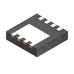
ICGOO电子元器件商城为您提供FDMC86012由Fairchild Semiconductor设计生产,在icgoo商城现货销售,并且可以通过原厂、代理商等渠道进行代购。 FDMC86012价格参考。Fairchild SemiconductorFDMC86012封装/规格:晶体管 - FET,MOSFET - 单, 表面贴装 N 沟道 30V 23A(Ta) 2.3W(Ta),54W(Tc) Power33。您可以下载FDMC86012参考资料、Datasheet数据手册功能说明书,资料中有FDMC86012 详细功能的应用电路图电压和使用方法及教程。
FDMC86012 是由 ON Semiconductor(安森美半导体)生产的一款 N 沟道增强型 MOSFET(金属-氧化物-半导体场效应晶体管)。该器件广泛应用于多种电力电子应用场景中,尤其适合需要高效开关和低导通电阻的场合。以下是其主要应用场景:

 1. 电源管理
   FDMC86012 常用于 DC-DC 转换器、开关电源 (SMPS) 和电池管理系统 (BMS) 中。由于其低导通电阻(Rds(on)),在高电流应用中能够显著降低功耗,提高效率。例如,在笔记本电脑、智能手机等便携式设备的充电电路中,它能有效减少发热,延长电池寿命。

 2. 电机驱动
   在电动工具、家用电器(如吸尘器、洗衣机)、以及工业自动化设备中的电机控制电路中,FDMC86012 可作为功率开关使用。它能够快速响应驱动信号,实现精确的电机调速和启停控制,同时具备良好的耐压性能,确保系统稳定运行。

 3. 负载切换
   该 MOSFET 适用于负载切换应用,如汽车电子中的继电器替代方案。它可以实现对大电流负载的快速接通与断开操作,具有较低的开关损耗和较高的可靠性,特别适合汽车启动系统、LED 照明控制等场景。

 4. 保护电路
   FDMC86012 还可用于过流保护、短路保护等安全电路设计中。通过检测异常电流并迅速切断电路,防止后端电路因过载而损坏,保障整个系统的安全性。

 5. 逆变器
   在太阳能逆变器、不间断电源 (UPS) 等电力转换设备中,FDMC86012 可作为关键的功率开关元件,帮助实现直流到交流的高效转换,提升能源利用效率。

总之,FDMC86012 凭借其优异的电气特性,成为众多电力电子设备中不可或缺的关键组件,尤其是在对效率、可靠性和成本敏感的应用领域表现尤为突出。
| 参数 | 数值 |
| 产品目录 | |
| ChannelMode | Depletion |
| 描述 | MOSFET N-CH 100V 23A 8MLPMOSFET 30V N-Channel PowerTrench MOSFET |
| 产品分类 | FET - 单分离式半导体 |
| FET功能 | 逻辑电平门 |
| FET类型 | MOSFET N 通道,金属氧化物 |
| Id-ContinuousDrainCurrent | 88 A |
| Id-连续漏极电流 | 88 A |
| 品牌 | Fairchild Semiconductor |
| 产品手册 | |
| 产品图片 |
|
| rohs | 符合RoHS无铅 / 符合限制有害物质指令(RoHS)规范要求 |
| 产品系列 | 晶体管,MOSFET,Fairchild Semiconductor FDMC86012PowerTrench® |
| 数据手册 | |
| 产品型号 | FDMC86012 |
| Pd-PowerDissipation | 54 W |
| Pd-功率耗散 | 54 W |
| Qg-GateCharge | 27 nC |
| Qg-栅极电荷 | 27 nC |
| RdsOn-Drain-SourceResistance | 2.7 mOhms |
| RdsOn-漏源导通电阻 | 2.7 mOhms |
| Vds-Drain-SourceBreakdownVoltage | 30 V |
| Vds-漏源极击穿电压 | 30 V |
| Vgs-Gate-SourceBreakdownVoltage | 12 V |
| Vgs-栅源极击穿电压 | 12 V |
| Vgsth-Gate-SourceThresholdVoltage | 1 V |
| Vgsth-栅源极阈值电压 | 1 V |
| 上升时间 | 11 ns |
| 下降时间 | 8 ns |
| 不同Id时的Vgs(th)(最大值) | 1.5V @ 250µA |
| 不同Vds时的输入电容(Ciss) | 5075pF @ 15V |
| 不同Vgs时的栅极电荷(Qg) | 38nC @ 4.5V |
| 不同 Id、Vgs时的 RdsOn(最大值) | 2.7 mOhm @ 23A, 4.5V |
| 产品种类 | MOSFET |
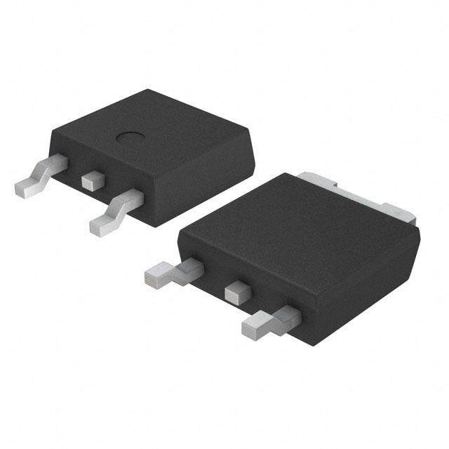
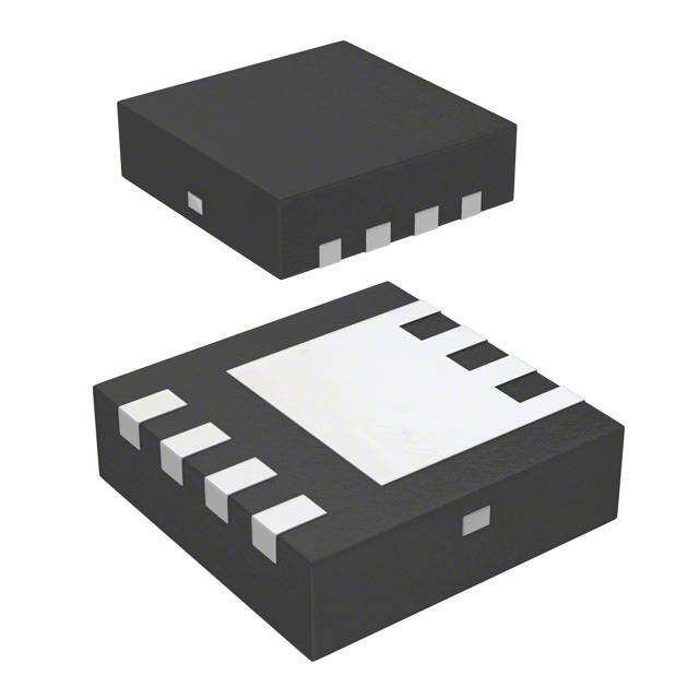
| 供应商器件封装 | Power33 |
| 其它名称 | FDMC86012DKR |
| 典型关闭延迟时间 | 43 ns |
| 功率-最大值 | 2.3W |
| 包装 | Digi-Reel® |
| 单位重量 | 152.700 mg |
| 商标 | Fairchild Semiconductor |
| 安装类型 | 表面贴装 |
| 安装风格 | SMD/SMT |
| 导通电阻 | 2.7 mOhms |
| 封装 | Reel |
| 封装/外壳 | 8-WDFN 裸露焊盘 |
| 封装/箱体 | Power 33-8 |
| 工厂包装数量 | 3000 |
| 晶体管极性 | N-Channel |
| 最大工作温度 | + 150 C |
| 最小工作温度 | - 55 C |
| 标准包装 | 1 |
| 正向跨导-最小值 | 144 S |
| 汲极/源极击穿电压 | 30 V |
| 漏极连续电流 | 88 A |
| 漏源极电压(Vdss) | 30V |
| 电流-连续漏极(Id)(25°C时) | 23A (Ta) |
| 系列 | FDMC86012 |
| 通道模式 | Depletion |
| 配置 | Single Quad Drain Triple Source |


PDF Datasheet 数据手册内容提取
Is Now Part of To learn more about ON Semiconductor, please visit our website at www.onsemi.com Please note: As part of the Fairchild Semiconductor integration, some of the Fairchild orderable part numbers will need to change in order to meet ON Semiconductor’s system requirements. Since the ON Semiconductor product management systems do not have the ability to manage part nomenclature that utilizes an underscore (_), the underscore (_) in the Fairchild part numbers will be changed to a dash (-). This document may contain device numbers with an underscore (_). Please check the ON Semiconductor website to verify the updated device numbers. The most current and up-to-date ordering information can be found at www.onsemi.com. Please email any questions regarding the system integration to Fairchild_questions@onsemi.com. ON Semiconductor and the ON Semiconductor logo are trademarks of Semiconductor Components Industries, LLC dba ON Semiconductor or its subsidiaries in the United States and/or other countries. ON Semiconductor owns the rights to a number of patents, trademarks, copyrights, trade secrets, and other intellectual property. A listing of ON Semiconductor’s product/patent coverage may be accessed at www.onsemi.com/site/pdf/Patent-Marking.pdf. ON Semiconductor reserves the right to make changes without further notice to any products herein. ON Semiconductor makes no warranty, representation or guarantee regarding the suitability of its products for any particular purpose, nor does ON Semiconductor assume any liability arising out of the application or use of any product or circuit, and specifically disclaims any and all liability, including without limitation special, consequential or incidental damages. Buyer is responsible for its products and applications using ON Semiconductor products, including compliance with all laws, regulations and safety requirements or standards, regardless of any support or applications information provided by ON Semiconductor. “Typical” parameters which may be provided in ON Semiconductor data sheets and/or specifications can and do vary in different applications and actual performance may vary over time. All operating parameters, including “Typicals” must be validated for each customer application by customer’s technical experts. ON Semiconductor does not convey any license under its patent rights nor the rights of others. ON Semiconductor products are not designed, intended, or authorized for use as a critical component in life support systems or any FDA Class 3 medical devices or medical devices with a same or similar classification in a foreign jurisdiction or any devices intended for implantation in the human body. Should Buyer purchase or use ON Semiconductor products for any such unintended or unauthorized application, Buyer shall indemnify and hold ON Semiconductor and its officers, employees, subsidiaries, affiliates, and distributors harmless against all claims, costs, damages, and expenses, and reasonable attorney fees arising out of, directly or indirectly, any claim of personal injury or death associated with such unintended or unauthorized use, even if such claim alleges that ON Semiconductor was negligent regarding the design or manufacture of the part. ON Semiconductor is an Equal Opportunity/Affirmative Action Employer. This literature is subject to all applicable copyright laws and is not for resale in any manner.
F D M C 8 October 2012 6 0 1 FDMC86012 2 N N-Channel Power Trench® MOSFET -C h 30 V, 88 A, 2.7 mΩ a n Features General Description n e l (cid:132) Max rDS(on) = 2.7 mΩ at VGS = 4.5 V, ID = 23 A This device has been designed specifically to improve the P efficiency of DC/DC converters. Using new techniques in o (cid:132) Max rDS(on) = 4.7 mΩ at VGS = 2.5 V, ID = 17.5 A MOSFET construction, the various components of gate charge w (cid:132) High performance technology for extremely low r and capacitance have been optimized to reduce switching e DS(on) r losses. Low gate resistance and very low Miller charge enable T (cid:132) Termination is Lead-free excellent performance with both adaptive and fixed dead time r e (cid:132) 100% UIL Tested gate drive circuits. Very low rDS(on) has been maintained to n provide a sub logic-level device. c (cid:132) RoHS Compliant h Applications ® M (cid:132) 3.3 V input synchronous buck switch O (cid:132) Synchronous rectifier S F E T Pin 1 Pin 1 S S S D S G S D S D D D D D G D Top Bottom Power 33 MOSFET Maximum Ratings TA = 25 °C unless otherwise noted Symbol Parameter Ratings Units V Drain to Source Voltage 30 V DS V Gate to Source Voltage ±12 V GS Drain Current -Continuous T = 25 °C 88 C ID -Continuous TA = 25 °C (Note 1a) 23 A -Pulsed (Note 4) 230 E Single Pulse Avalanche Energy (Note 3) 337 mJ AS Power Dissipation T = 25 °C 54 P C W D Power Dissipation T = 25 °C (Note 1a) 2.3 A T , T Operating and Storage Junction Temperature Range -55 to +150 °C J STG Thermal Characteristics R Thermal Resistance, Junction to Case (Note 1) 2.3 θJC °C/W R Thermal Resistance, Junction to Ambient (Note 1a) 53 θJA Package Marking and Ordering Information Device Marking Device Package Reel Size Tape Width Quantity FDMC86012 FDMC86012 Power33 13 ’’ 12 mm 3000 units ©2012 Fairchild Semiconductor Corporation 1 www.fairchildsemi.com FDMC86012 Rev. C
F D Electrical Characteristics M T = 25 °C unless otherwise noted J C Symbol Parameter Test Conditions Min Typ Max Units 8 6 0 Off Characteristics 1 2 BVDSS Drain to Source Breakdown Voltage ID = 250 μA, VGS = 0 V 30 V N ΔBVDSS Breakdown Voltage Temperature I = 250 μA, referenced to 25 °C 43 mV/°C -C ΔT Coefficient D J h I Zero Gate Voltage Drain Current V = 24 V, V = 0 V 1 μA a DSS DS GS n IGSS Gate to Source Leakage Current VGS = ±12 V, VDS = 0 V ±100 nA n e l On Characteristics P o VGS(th) Gate to Source Threshold Voltage VGS = VDS, ID = 250 μA 0.8 1.0 1.5 V w ΔV Gate to Source Threshold Voltage e ΔTGJS(th) Temperature Coefficient ID = 250 μA, referenced to 25 °C -4 mV/°C r T V = 4.5 V, I = 23 A 2.2 2.7 r GS D e r Static Drain to Source On Resistance V = 2.5 V, I = 17.5 A 3.4 4.7 mΩ n DS(on) GS D c VGS = 4.5 V, ID = 23 A, TJ = 125 °C 3.5 4.3 h ® g Forward Transconductance V = 5 V, I = 23 A 144 S FS DD D M Dynamic Characteristics O S Ciss Input Capacitance 3625 5075 pF F C Output Capacitance VDS = 15 V, VGS = 0 V, 1230 1725 pF E oss f = 1 MHz T C Reverse Transfer Capacitance 185 260 pF rss R Gate Resistance 0.1 0.9 3.0 Ω g Switching Characteristics t Turn-On Delay Time 20 32 ns d(on) tr Rise Time VDD = 15 V, ID = 23 A, 11 20 ns td(off) Turn-Off Delay Time VGS = 4.5 V, RGEN = 6 Ω 43 69 ns t Fall Time 8 16 ns f Q Total Gate Charge V = 0 V to 4.5 V 27 38 nC g(TOT) GS Qg(TOT) Total Gate Charge VGS = 0 V to 2.5 V VDD = 15 V, 16 23 nC Qgs Gate to Source Charge ID = 23 A 5.8 nC Q Gate to Drain “Miller” Charge 5.4 nC gd Drain-Source Diode Characteristics V = 0 V, I = 23 A (Note 2) 0.8 1.3 V V Source to Drain Diode Forward Voltage GS S SD V = 0 V, I = 1.9 A (Note 2) 0.7 1.2 V GS S t Reverse Recovery Time 40 64 ns rr I = 23 A, di/dt = 100 A/μs Q Reverse Recovery Charge F 23 37 nC rr Notes: 1. RθJA is determined with the device mounted on a 1 in2 pad 2 oz copper pad on a 1.5 x 1.5 in. board of FR-4 material. RθJC is guaranteed by design while RθCA is determined by the user's board design. a. 53 °C/W when mounted on a b.125 °C/W when mounted on a 1 in2 pad of 2 oz copper minimum pad of 2 oz copper GDDSS FSFS GDDSS FSFS 2. Pulse Test: Pulse Width < 300 μs, Duty cycle < 2.0%. 3. EAS of 337 mJ is based on starting TJ = 25 °C; N-ch: L = 3 mH, IAS = 15 A, VDD = 30 V, VGS = 10 V. 100% test at L = 0.3 mH, IAS = 33 A. 4. Pulsed Id limited by junction temperature,td<=100uS, please refer to SOA curve for more details. ©2012 Fairchild Semiconductor Corporation 2 www.fairchildsemi.com FDMC86012 Rev. C
F D M Typical Characteristics TJ = 25 °C unless otherwise noted C 8 6 230 6 0 VGS = 10 V NCE PDUULTSYE C DYUCRLEA T=I O0.N5 %= 8M0A μXs 12 A 5 184 T N NT (A) VGS = 4.5 V VGS = 2.5 V DRESIS 4 VGS = 2 V -Ch , DRAIN CURRED1349862 VGS = 3 V VGS = 2 V NORMALIZEN TO SOURCE ON- 123 VGS = 3V VGS = 2.5 V VGS = 4.5 V annelPow I PDUULTSYE C DYUCRLEA T=I O0.N5 %= 8M0A μXs RAI VGS = 10 V er 0 D 0 T 0 1 2 3 4 5 0 46 92 138 184 230 r VDS, DRAIN TO SO URCE VOLTAGE (V) ID, DRAIN C URRENT (A) en c Figure 1. On-Region Characteristics Figure 2. Normalized On-Resistance h ® vs Drain Current and Gate Voltage M O 1.8 15 ALIZEDE ON-RESISTANCE111...246 IVDG =S 2=3 4 A.5 V DRAIN TO ()mESISTANCE Ω129 PDUULTSYE C DYUCRLEA T=I OI0D.N 5= % =2 38M 0AA μXs SFET NORM N TO SOURC01..80 r,DS(on)OURCE ON-R 36 TJ = 125 oC RAI S TJ = 25 oC D0.6 0 -75 -50 -25 0 25 50 75 100 125 150 1.5 2.0 2.5 3.0 3.5 4.0 4.5 TJ, JUNCTION TEM PERATURE (oC) VGS, GATE TO SO URCE VOLTAGE (V) Figure 3. Normalized On- Resistance Figure 4. On-Resistance vs Gate to vs Junction Temperature Source Voltage 230 500 PULSE DURATION = 80 μs A) VGS = 0 V DUTY CYCLE = 0.5% MAX T ( 100 184 N E T (A) VDS = 5 V URR 10 RREN138 AIN C 1 TJ = 150 oC CU TJ = 150 oC DR RAIN 92 TJ = 25 oC ERSE 0.1 TJ = 25 oC D V I, D 46 TJ = -55 oC I, RES0.01 TJ = -55 oC 0 0.001 0 1 2 3 4 0.0 0.2 0.4 0.6 0.8 1.0 1.2 VGS, GATE TO SOU RCE VOLTAGE (V) VSD, BODY DIODE FOR WARD VOLTAGE (V) Figure 5. Transfer Characteristics Figure 6. Source to Drain Diode Forward Voltage vs Source Current ©2012 Fairchild Semiconductor Corporation 3 www.fairchildsemi.com FDMC86012 Rev. C
F D M Typical Characteristics T = 25 °C unless otherwise noted J C 8 4.5 10000 6 0 E (V) ID = 23 A VDD = 10 V 12 AG3.6 Ciss N OLT VDD = 15 V pF)1000 -C SOURCE V12..87 VDD = 20 V CITANCE ( Coss hanne E TO CAPA 100 Crss lP T0.9 o V, GAGS0.0 10 fV =G S1 =M 0H Vz wer 0 6 12 18 24 30 0.1 1 10 30 T r Qg, GATE CH ARGE (nC) VDS, DRAIN TO SOU RCE VOLTAGE (V) e n c Figure 7. Gate Charge Characteristics Figure 8. Capacitance vs Drain h ® to Source Voltage M 100 120 O RθJC = 2.3 oC/W SF NT (A) T (A) 90 ET E N R E E CUR 10 TJ = 25 oC CURR 60 VGS = 4.5V VALANCH TJ = 125 oC TJ = 100 oC , IDRAIN D 30 Limited by Package VGS = 2.5 V A , S A I 1 0 0.001 0.01 0.1 1 10 100 500 25 50 75 100 125 150 tAV, TIME IN AVA LANCHE (ms) TC, CASE TEMPERATURE (oC) Figure 9. Unclamped Inductive Figure 10. Maximum Continuous Drain Switching Capability Current vs Case Temperature 300 2000 100 W)1000 SINGLE PULSE NT (A) 10 100 us POWER ( 100 TRAθJ =A 2=5 1 o2C5 oC/W N CURRE 1 TLHIMISIT AERDE BAY I Sr 110 m mss ANSIENT 10 AI DS(on) 100 ms R DR SINGLE PULSE K T I, D00.0.11 TRTJAθ J ==A M2=5 A1 oX2C5 R oACT/WED CMUERAVSEU RBEEDN TD ATOTA 11D 0Cs s , PPEA()PK 0.11 0.01 0.1 1 10 100200 10-4 10-3 10-2 10-1 1 10 100 1000 VDS, DRAIN to SOU RCE VOLTAGE (V) t, PULSE WI DTH (sec) Figure 11. Forward Bias Safe Figure 12. Single Pulse Maximum Operating Area Power Dissipation ©2012 Fairchild Semiconductor Corporation 4 www.fairchildsemi.com FDMC86012 Rev. C
F D M Typical Characteristics T = 25 °C unless otherwise noted J C 8 2 6 1 0 DUTY CYCLE-DESCENDING ORDER 1 2 D = 0.5 L 0.2 N MA A 0.1 0.1 -C NORMALIZED THER ZIMPEDANCE,Jθ 00..0011 000...000521 SRIθNJAG =L E1 2P5U oLCS/EW NDPEOUATTYKE S FT:AJ C= TPODRM: xD Z =Pθ JDtA1M /xt2 RθJAt1 +t T2A hannelPow e r T 0.001 10-4 10-3 10-2 10-1 1 10 100 1000 re n t, RECTANGULAR PULSE DURATION (sec) c Figure 13. Junction-to-Ambient Transient Thermal Response Curve h ® M O S F E T ©2012 Fairchild Semiconductor Corporation 5 www.fairchildsemi.com FDMC86012 Rev. C
F D Dimensional Outline and Pad Layout M C 8 6 0 1 2 N - C h a n n e l P o w e r T r e n c h ® M O S F E T ©2012 Fairchild Semiconductor Corporation 6 www.fairchildsemi.com FDMC86012 Rev. C
F D M C 8 6 0 1 2 TRADEMARKS N The following includes registered and unregistered trademarks and service marks, owned by Fairchild Semiconductor and/or its global subsidiaries, and is not - intended to be an exhaustive list of all such trademarks. C 2Cool™ F-PFS™ PowerTrench® The Power Franchise® ha AccuPower™ FRFET® PowerXS™ ® n AX-CAP™* Global Power ResourceSM Programmable Active Droop™ n BitSiC® Green Bridge™ QFET® e Build it Now™ Green FPS™ QS™ TTiinnyyBBouocks™t™ lP CorePLUS™ Green FPS™ e-Series™ Quiet Series™ TinyCalc™ o CorePOWER™ Gmax™ RapidConfigure™ TinyLogic® w CROSSVOLT™ GTO™ ™ CTL™ IntelliMAX™ TINYOPTO™ e TinyPower™ r Current Transfer Logic™ ISOPLANAR™ Saving our world, 1mW/W/kW at a time™ DEUXPEED® Marking Small Speakers Sound Louder SignalWise™ TinyPWM™ T TinyWire™ r DEcuoaSl CPoAoRl™K® aMnedg aBBeuttcekr™™ SSmMaArRtMTa SxT™ART™ TranSiC® en EEfSfiBceCn™tMax™ MMiIcCrRoFOECTO™UPLER™ SSoPlMut®ions for Your Success™ TTRriFUaEuClt UDReRteEcNt™T®* ch μSerDes™ ® MicroPak™ STEALTH™ ® MicroPak2™ SuperFET® M FFFFaaAAiiCCrrccTThh® iiQllddu® Sieet mSiecroiensd™uctor® MMMmioWolltteiiSoorDannvM-rSievaPrex™M™™™ SSSSuuuuppppeeererrrSSSMOOOOTTTS™™™®---368 UUUlHntriCFa E®FTR™FET™ OSFE FAST® OptoHiT™ SyncFET™ VCX™ T FastvCore™ OPTOLOGIC® Sync-Lock™ VisualMax™ FETBench™ OPTOPLANAR® ®* VoltagePlus™ FlashWriter® * XS™ ® FPS™ *Trademarks of System General Corporation, used under license by Fairchild Semiconductor. DISCLAIMER FAIRCHILD SEMICONDUCTOR RESERVES THE RIGHT TO MAKE CHANGES WITHOUT FURTHER NOTICE TO ANY PRODUCTS HEREIN TO IMPROVE RELIABILITY, FUNCTION, OR DESIGN. FAIRCHILD DOES NOT ASSUME ANY LIABILITY ARISING OUT OF THE APPLICATION OR USE OF ANY PRODUCT OR CIRCUIT DESCRIBED HEREIN; NEITHER DOES IT CONVEY ANY LICENSE UNDER ITS PATENT RIGHTS, NOR THE RIGHTS OF OTHERS. THESE SPECIFICATIONS DO NOT EXPAND THE TERMS OF FAIRCHILD’S WORLDWIDE TERMS AND CONDITIONS, SPECIFICALLY THE WARRANTY THEREIN, WHICH COVERS THESE PRODUCTS. LIFE SUPPORT POLICY FAIRCHILD’S PRODUCTS ARE NOT AUTHORIZED FOR USE AS CRITICAL COMPONENTS IN LIFE SUPPORT DEVICES OR SYSTEMS WITHOUT THE EXPRESS WRITTEN APPROVAL OF FAIRCHILD SEMICONDUCTOR CORPORATION. As used here in: 1. Life support devices or systems are devices or systems which, (a) are 2. A critical component in any component of a life support, device, or intended for surgical implant into the body or (b) support or sustain life, system whose failure to perform can be reasonably expected to cause and (c) whose failure to perform when properly used in accordance with the failure of the life support device or system, or to affect its safety or instructions for use provided in the labeling, can be reasonably effectiveness. expected to result in a significant injury of the user. ANTI-COUNTERFEITING POLICY Fairchild Semiconductor Corporation’s Anti-Counterfeiting Policy. Fairchild’s Anti-Counterfeiting Policy is also stated on our external website, www.Fairchildsemi.com, under Sales Support. Counterfeiting of semiconductor parts is a growing problem in the industry. All manufactures of semiconductor products are experiencing counterfeiting of their parts. Customers who inadvertently purchase counterfeit parts experience many problems such as loss of brand reputation, substandard performance, failed application, and increased cost of production and manufacturing delays. Fairchild is taking strong measures to protect ourselves and our customers from the proliferation of counterfeit parts. Fairchild strongly encourages customers to purchase Fairchild parts either directly from Fairchild or from Authorized Fairchild Distributors who are listed by country on our web page cited above. Products customers buy either from Fairchild directly or from Authorized Fairchild Distributors are genuine parts, have full traceability, meet Fairchild’s quality standards for handing and storage and provide access to Fairchild’s full range of up-to-date technical and product information. Fairchild and our Authorized Distributors will stand behind all warranties and will appropriately address and warranty issues that may arise. Fairchild will not provide any warranty coverage or other assistance for parts bought from Unauthorized Sources. Fairchild is committed to combat this global problem and encourage our customers to do their part in stopping this practice by buying direct or from authorized distributors. PRODUCT STATUS DEFINITIONS Definition of Terms Datasheet Identification Product Status Definition Datasheet contains the design specifications for product development. Specifications Advance Information Formative / In Design may change in any manner without notice. Datasheet contains preliminary data; supplementary data will be published at a later Preliminary First Production date. Fairchild Semiconductor reserves the right to make changes at any time without notice to improve design. Datasheet contains final specifications. Fairchild Semiconductor reserves the right to No Identification Needed Full Production make changes at any time without notice to improve the design. Datasheet contains specifications on a product that is discontinued by Fairchild Obsolete Not In Production Semiconductor. The datasheet is for reference information only. Rev. I61 ©2012 Fairchild Semiconductor Corporation 7 www.fairchildsemi.com FDMC86012 Rev. C
ON Semiconductor and are trademarks of Semiconductor Components Industries, LLC dba ON Semiconductor or its subsidiaries in the United States and/or other countries. ON Semiconductor owns the rights to a number of patents, trademarks, copyrights, trade secrets, and other intellectual property. A listing of ON Semiconductor’s product/patent coverage may be accessed at www.onsemi.com/site/pdf/Patent−Marking.pdf. ON Semiconductor reserves the right to make changes without further notice to any products herein. ON Semiconductor makes no warranty, representation or guarantee regarding the suitability of its products for any particular purpose, nor does ON Semiconductor assume any liability arising out of the application or use of any product or circuit, and specifically disclaims any and all liability, including without limitation special, consequential or incidental damages. Buyer is responsible for its products and applications using ON Semiconductor products, including compliance with all laws, regulations and safety requirements or standards, regardless of any support or applications information provided by ON Semiconductor. “Typical” parameters which may be provided in ON Semiconductor data sheets and/or specifications can and do vary in different applications and actual performance may vary over time. All operating parameters, including “Typicals” must be validated for each customer application by customer’s technical experts. ON Semiconductor does not convey any license under its patent rights nor the rights of others. ON Semiconductor products are not designed, intended, or authorized for use as a critical component in life support systems or any FDA Class 3 medical devices or medical devices with a same or similar classification in a foreign jurisdiction or any devices intended for implantation in the human body. Should Buyer purchase or use ON Semiconductor products for any such unintended or unauthorized application, Buyer shall indemnify and hold ON Semiconductor and its officers, employees, subsidiaries, affiliates, and distributors harmless against all claims, costs, damages, and expenses, and reasonable attorney fees arising out of, directly or indirectly, any claim of personal injury or death associated with such unintended or unauthorized use, even if such claim alleges that ON Semiconductor was negligent regarding the design or manufacture of the part. ON Semiconductor is an Equal Opportunity/Affirmative Action Employer. This literature is subject to all applicable copyright laws and is not for resale in any manner. PUBLICATION ORDERING INFORMATION LITERATURE FULFILLMENT: N. American Technical Support: 800−282−9855 Toll Free ON Semiconductor Website: www.onsemi.com Literature Distribution Center for ON Semiconductor USA/Canada 19521 E. 32nd Pkwy, Aurora, Colorado 80011 USA Europe, Middle East and Africa Technical Support: Order Literature: http://www.onsemi.com/orderlit Phone: 303−675−2175 or 800−344−3860 Toll Free USA/Canada Phone: 421 33 790 2910 Fax: 303−675−2176 or 800−344−3867 Toll Free USA/Canada Japan Customer Focus Center For additional information, please contact your local Email: orderlit@onsemi.com Phone: 81−3−5817−1050 Sales Representative © Semiconductor Components Industries, LLC www.onsemi.com www.onsemi.com 1
Mouser Electronics Authorized Distributor Click to View Pricing, Inventory, Delivery & Lifecycle Information: O N Semiconductor: FDMC86012