ICGOO在线商城 > 分立半导体产品 > 晶体管 - FET,MOSFET - 单 > NTMFS4927NT1G
 Datasheet下载
- 型号: NTMFS4927NT1G
- 制造商: ON Semiconductor
- 库位|库存: xxxx|xxxx
- 要求:
| 数量阶梯 | 香港交货 | 国内含税 |
| +xxxx | $xxxx | ¥xxxx |
查看当月历史价格
查看今年历史价格
NTMFS4927NT1G产品简介:
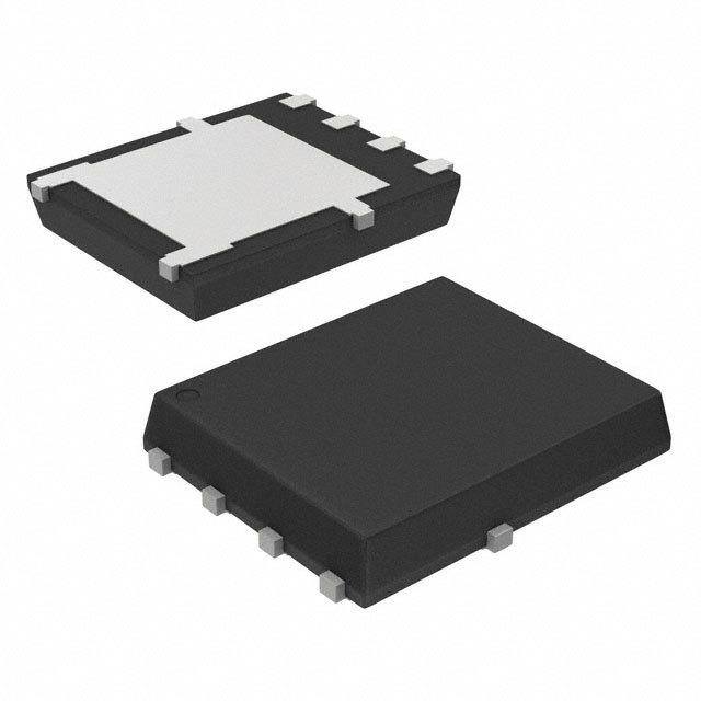
ICGOO电子元器件商城为您提供NTMFS4927NT1G由ON Semiconductor设计生产,在icgoo商城现货销售,并且可以通过原厂、代理商等渠道进行代购。 NTMFS4927NT1G价格参考¥1.64-¥1.74。ON SemiconductorNTMFS4927NT1G封装/规格:晶体管 - FET,MOSFET - 单, 表面贴装 N 沟道 30V 7.9A(Ta),38A(Tc) 920mW(Ta),20.8W(Tc) 5-DFN(5x6)(8-SOFL)。您可以下载NTMFS4927NT1G参考资料、Datasheet数据手册功能说明书,资料中有NTMFS4927NT1G 详细功能的应用电路图电压和使用方法及教程。
NTMFS4927NT1G 是一款由 ON Semiconductor(安森美半导体)生产的 N 沟道增强型 MOSFET,属于晶体管 - FET、MOSFET - 单类别。该型号具有低导通电阻(Rds(on))、高开关速度和良好的热性能,适用于多种电力电子应用场景。以下是其主要的应用领域:

1. 电源管理
   NTMFS4927NT1G 常用于开关电源(SMPS)、DC-DC 转换器和电压调节模块(VRM)。其低 Rds(on) 特性能够减少传导损耗,提高效率,适合笔记本电脑、台式机和其他消费电子设备中的电源管理系统。

2. 电机驱动
   该 MOSFET 可用于小型直流电机的驱动电路中,例如风扇、泵或玩具电机。其快速开关能力和低导通电阻有助于实现高效且稳定的电机控制。

3. 负载开关
   在需要动态控制电流流动的场景中,如 USB 充电端口保护、电池管理系统等,NTMFS4927NT1G 可作为负载开关使用,提供高效的电流切换功能。

4. 电池保护与管理
   它可用于锂离子电池或其他可充电电池组的保护电路中,防止过流、短路或过度放电等问题。其低导通电阻有助于降低电池系统的功耗。

5. 通信设备
   在网络路由器、交换机和基站等通信设备中,该 MOSFET 可用于信号调理、功率分配和电源转换等任务,确保设备稳定运行。

6. 汽车电子
   尽管 NTMFS4927NT1G 主要针对工业和消费类应用,但在某些非关键性车载系统中(如车窗升降器、座椅调节器等),它也可用作驱动元件。

总结来说,NTMFS4927NT1G 凭借其优异的电气特性和可靠性,广泛应用于消费电子、工业自动化、通信设备以及轻型汽车电子等领域,为各种电力转换和控制需求提供支持。
| 参数 | 数值 |
| 产品目录 | |
| 描述 | MOSFET N-CH 30V 7.9A SO-8FLMOSFET TRENCH 3.1 30V 9 Ohm NCH |
| 产品分类 | FET - 单分离式半导体 |
| FET功能 | 逻辑电平门 |
| FET类型 | MOSFET N 通道,金属氧化物 |
| Id-ContinuousDrainCurrent | 38 A |
| Id-连续漏极电流 | 38 A |
| 品牌 | ON Semiconductor |
| 产品手册 | |
| 产品图片 |
|
| rohs | 符合RoHS无铅 / 符合限制有害物质指令(RoHS)规范要求 |
| 产品系列 | 晶体管,MOSFET,ON Semiconductor NTMFS4927NT1G- |
| 数据手册 | |
| 产品型号 | NTMFS4927NT1G |
| Pd-PowerDissipation | 0.92 W, 2.7 W, 6.04 W, 20.8 W |
| Pd-功率耗散 | 20.8 W |
| Qg-GateCharge | 8 nC |
| Qg-栅极电荷 | 8 nC |
| RdsOn-Drain-SourceResistance | 13.5 mOhms |
| RdsOn-漏源导通电阻 | 13.5 mOhms |
| Vds-Drain-SourceBreakdownVoltage | 30 V |
| Vds-漏源极击穿电压 | 30 V |
| Vgsth-Gate-SourceThresholdVoltage | 1.6 V |
| Vgsth-栅源极阈值电压 | 1.6 V |
| 不同Id时的Vgs(th)(最大值) | 2.2V @ 250µA |
| 不同Vds时的输入电容(Ciss) | 913pF @ 15V |
| 不同Vgs时的栅极电荷(Qg) | 16nC @ 10V |
| 不同 Id、Vgs时的 RdsOn(最大值) | 7.3 毫欧 @ 30A,10V |
| 产品种类 | MOSFET |
| 供应商器件封装 | 5-DFN, 8-SO 扁引线 (5x6) |
| 其它名称 | NTMFS4927NT1GOSDKR |
| 功率-最大值 | 920mW |
| 功率耗散 | 0.92 W, 2.7 W, 6.04 W, 20.8 W |
| 包装 | Digi-Reel® |
| 商标 | ON Semiconductor |
| 安装类型 | 表面贴装 |
| 安装风格 | SMD/SMT |
| 导通电阻 | 13.5 mOhms |
| 封装 | Reel |
| 封装/外壳 | 8-PowerTDFN, 5 引线 |
| 封装/箱体 | SO-8FL |
| 工厂包装数量 | 1500 |
| 晶体管极性 | N-Channel |
| 最大工作温度 | + 150 C |
| 最小工作温度 | - 55 C |
| 栅极电荷Qg | 8 nC |
| 标准包装 | 1 |
| 正向跨导-最小值 | 40 s |
| 汲极/源极击穿电压 | 30 V |
| 漏极连续电流 | 38 A |
| 漏源极电压(Vdss) | 30V |
| 电流-连续漏极(Id)(25°C时) | 7.9A (Ta), 38A (Tc) |
| 系列 | NTMFS4927N |
| 配置 | Single |


- 商务部:美国ITC正式对集成电路等产品启动337调查
- 曝三星4nm工艺存在良率问题 高通将骁龙8 Gen1或转产台积电
- 太阳诱电将投资9.5亿元在常州建新厂生产MLCC 预计2023年完工
- 英特尔发布欧洲新工厂建设计划 深化IDM 2.0 战略
- 台积电先进制程称霸业界 有大客户加持明年业绩稳了
- 达到5530亿美元!SIA预计今年全球半导体销售额将创下新高
- 英特尔拟将自动驾驶子公司Mobileye上市 估值或超500亿美元
- 三星加码芯片和SET,合并消费电子和移动部门,撤换高东真等 CEO
- 三星电子宣布重大人事变动 还合并消费电子和移动部门
- 海关总署:前11个月进口集成电路产品价值2.52万亿元 增长14.8%


PDF Datasheet 数据手册内容提取
NTMFS4927N, NTMFS4927NC Power MOSFET 30 V, 38 A, Single N−Channel, SO−8 FL Features • Low R to Minimize Conduction Losses DS(on) • Low Capacitance to Minimize Driver Losses • Optimized Gate Charge to Minimize Switching Losses http://onsemi.com • Optimized for 5 V, 12 V Gate Drives • These Devices are Pb−Free, Halogen Free/BFR Free and are RoHS V(BR)DSS RDS(ON) MAX ID MAX Compliant 7.3 m(cid:4) @ 10 V Applications 30 V 38 A • CPU Power Delivery 12.0 m(cid:4) @ 4.5 V • DC−DC Converters D (5,6) MAXIMUM RATINGS (TJ = 25°C unless otherwise stated) Parameter Symbol Value Unit Drain−to−Source Voltage VDSS 30 V Gate−to−Source Voltage VGS ±20 V G (4) Continuous Drain TA = 25°C ID 13.6 A C(Nuortree n1t) R(cid:2)JA TA = 100°C 8.6 S (1,2,3) Power Dissipation TA = 25°C PD 2.70 W N−CHANNEL MOSFET R(cid:2)JA (Note 1) Continuous Drain TA = 25°C ID 20.4 A MARKING C(Nuortree n1t) R(cid:2)JA ≤ 10 s TA = 100°C 12.9 DIAGRAM Power Dissipation TA = 25°C PD 6.04 W D R(cid:2)JA ≤ 10 s (Note 1) Steady 1 S D CC(Nouonrtrteein n2ut) oRu(cid:2)sJ ADrain State TTAA = = 1 2050°°CC ID 75..90 A SOC−A8S FEL A48T8 LAEAAD GSS A4Y9W27ZNZ D STYLE 1 Power Dissipation TA = 25°C PD 0.92 W D R(cid:2)JA (Note 2) 4927N = Specific Device Code Continuous Drain TC = 25°C ID 38 A A = Assembly Location C(Nuortree n1t) R(cid:2)JC TC =100°C 24 YW == YWeoarrk Week Power Dissipation TC = 25°C PD 20.8 W ZZ = Lot Traceability R(cid:2)JC (Note 1) Pulsed Drain TA = 25°C, tp = 10 (cid:3)s IDM 160 A Current ORDERING INFORMATION Current Limited by Package TA = 25°C IDmax 100 A Device Package Shipping† Operating Junction and Storage TJ, −55 to °C Temperature TSTG +150 NTMFS4927NT1G SO−8 FL 1500 / Source Current (Body Diode) IS 21 A NTMFS4927NCT1G (Pb−Free) Tape & Reel Drain to Source DV/DT dV/dt 6.0 V/ns NTMFS4927NT3G SO−8 FL 5000 / Single Pulse Drain−to−Source Avalanche EAS 20 mJ NTMFS4927NCT3G (Pb−Free) Tape & Reel Energy (TJ = 25°C, VDD = 24 V, VGS = 20 V, †For information on tape and reel specifications, IL = 20 Apk, L = 0.1 mH, RG = 25 (cid:4)) including part orientation and tape sizes, please Lead Temperature for Soldering Purposes TL 260 °C refer to our Tape and Reel Packaging Specifications (1/8″ from case for 10 s) Brochure, BRD8011/D. Stresses exceeding Maximum Ratings may damage the device. Maximum Ratings are stress ratings only. Functional operation above the Recommended Operating Conditions is not implied. Extended exposure to stresses above the Recommended Operating Conditions may affect device reliability. 1. Surface−mounted on FR4 board using 1 sq−in pad, 1 oz Cu. 2. Surface−mounted on FR4 board using the minimum recommended pad size. © Semiconductor Components Industries, LLC, 2012 1 Publication Order Number: June, 2012 − Rev. 8 NTMFS4927N/D
NTMFS4927N, NTMFS4927NC THERMAL RESISTANCE MAXIMUM RATINGS Parameter Symbol Value Unit Junction−to−Case (Drain) R(cid:2)JC 6.0 Junction−to−Ambient – Steady State (Note 3) R(cid:2)JA 46.3 °C/W Junction−to−Ambient – Steady State (Note 4) R(cid:2)JA 136.2 Junction−to−Ambient – (t ≤ 10 s) (Note 3) R(cid:2)JA 20.7 3. Surface−mounted on FR4 board using 1 sq−in pad, 1 oz Cu. 4. Surface−mounted on FR4 board using the minimum recommended pad size. ELECTRICAL CHARACTERISTICS (TJ = 25°C unless otherwise specified) Parameter Symbol Test Condition Min Typ Max Unit OFF CHARACTERISTICS Drain−to−Source Breakdown Voltage V(BR)DSS VGS = 0 V, ID = 250 (cid:3)A 30 V Drain−to−Source Breakdown Voltage V(BR)DSSt VGS = 0 V, ID(aval) = 8.4 A, 34 V (transient) Tcase = 25°C, ttransient = 100 ns Drain−to−Source Breakdown Voltage V(BR)DSS/ 24 mV/°C Temperature Coefficient TJ Zero Gate Voltage Drain Current IDSS VGS = 0 V, TJ = 25°C 1.0 VDS = 24 V TJ = 125°C 10 (cid:3)A Gate−to−Source Leakage Current IGSS VDS = 0 V, VGS = ±20 V ±100 nA ON CHARACTERISTICS (Note 5) Gate Threshold Voltage VGS(TH) VGS = VDS, ID = 250 (cid:3)A 1.32 1.6 2.2 V Negative Threshold Temperature Coefficient VGS(TH)/TJ 3.7 mV/°C Drain−to−Source On Resistance RDS(on) VGS = 10 V ID = 30 A 5.8 7.3 ID = 15 A 5.7 m(cid:4) VGS = 4.5 V ID = 30 A 9.6 12 ID = 15 A 9.2 Forward Transconductance gFS VDS = 1.5 V, ID = 15 A 40 S CHARGES, CAPACITANCES & GATE RESISTANCE Input Capacitance CISS 913 Output Capacitance COSS VGS = 0 V, f = 1 MHz, VDS = 15 V 366 pF Reverse Transfer Capacitance CRSS 108 Capacitance Ratio CRSS / VGS = 0 V, VDS = 15 V, f = 1 MHz 0.118 0.237 CISS Total Gate Charge QG(TOT) 8.0 Threshold Gate Charge QG(TH) 1.6 VGS = 4.5 V, VDS = 15 V; ID = 30 A nC Gate−to−Source Charge QGS 3.1 Gate−to−Drain Charge QGD 3.1 Total Gate Charge QG(TOT) VGS = 10 V, VDS = 15 V; ID = 30 A 16.0 nC SWITCHING CHARACTERISTICS (Note 6) Turn−On Delay Time td(ON) 9.2 RTuisren −TOimff eDelay Time td(OtrFF) VGIDS == 145.5 A V, ,R VGD S= =3 .105 (cid:4) V, 2154..50 ns Fall Time tf 4.4 5. Pulse Test: pulse width (cid:2) 300 (cid:3)s, duty cycle (cid:2) 2%. 6. Switching characteristics are independent of operating junction temperatures. http://onsemi.com 2
NTMFS4927N, NTMFS4927NC ELECTRICAL CHARACTERISTICS (TJ = 25°C unless otherwise specified) Parameter Symbol Test Condition Min Typ Max Unit SWITCHING CHARACTERISTICS (Note 6) Turn−On Delay Time td(ON) 6.5 RTuisren −TOimff eDelay Time td(OtrFF) VIGDS = = 1 150 A V, ,R VGD S= =3 .105 (cid:4) V, 2118..00 ns Fall Time tf 3.0 DRAIN−SOURCE DIODE CHARACTERISTICS Forward Diode Voltage VSD VGS = 0 V, TJ = 25°C 0.87 1.1 V IS = 30 A TJ = 125°C 0.76 Reverse Recovery Time tRR 21.4 Charge Time ta VGS = 0 V, dIS/dt = 100 A/(cid:3)s, 10.5 ns Discharge Time tb IS = 30 A 10.9 Reverse Recovery Charge QRR 8.4 nC PACKAGE PARASITIC VALUES Source Inductance LS 1.00 nH Drain Inductance LD 0.005 nH TA = 25°C Gate Inductance LG 1.84 nH Gate Resistance RG 0.90 2.2 (cid:4) 5. Pulse Test: pulse width (cid:2) 300 (cid:3)s, duty cycle (cid:2) 2%. 6. Switching characteristics are independent of operating junction temperatures. http://onsemi.com 3
NTMFS4927N, NTMFS4927NC TYPICAL CHARACTERISTICS 100 100 90 10 V 4.5 V 90 TJ = −55°C A) 80 TJ = 25°C 4.0 V A) 80 TJ = 25°C T ( 70 T ( 70 N N RE 60 3.5 V RE 60 VDS = 10 V TJ = 125°C R R U 50 U 50 C C N 40 N 40 AI AI R 3.0 V R D 30 D 30 I, D 20 I, D 20 10 VGS = 2.5 V 10 0 0 0 1 2 3 4 5 1 2 3 4 5 VDS, DRAIN−TO−SOURCE VOLTAGE (V) VGS, GATE−TO−SOURCE VOLTAGE (V) Figure 1. On−Region Characteristics Figure 2. Transfer Characteristics (cid:4)) (cid:4)) E (0.015 E ( 0.019 C C AN0.014 ID = 30 A AN 0.017 T = 25°C T T S0.013 S SI SI 0.015 E0.012 E R R E 0.011 E 0.013 C C UR0.010 UR 0.011 VGS = 4.5 V SO0.009 SO O−0.008 O− 0.009 T T N−0.007 N− 0.007 RAI0.006 RAI VGS = 10 V D D 0.005 , DS(on)00..0000453 4 5 6 7 8 9 10, DS(on)0.00310 20 30 40 50 60 70 80 90 100 R R VGS (V) ID, DRAIN CURRENT (A) Figure 3. On−Resistance vs. V Figure 4. On−Resistance vs. Drain Current and GS Gate Voltage 1.7 10,000 RCEZED)11..65 IVDG =S 3=0 1 A0 V TJ = 150°C RAIN−TO−SOUCE (NORMALI1111....1243 LEAKAGE (nA)1,000 TJ = 125°C , DDS(on)ESISTAN001...980 I, DSS 100 TJ = 85°C RR 0.7 VGS = 0 V 0.6 10 −50 −25 0 25 50 75 100 125 150 5 10 15 20 25 30 TJ, JUNCTION TEMPERATURE (°C) VDS, DRAIN−TO−SOURCE VOLTAGE (V) Figure 5. On−Resistance Variation with Figure 6. Drain−to−Source Leakage Current Temperature vs. Voltage http://onsemi.com 4
NTMFS4927N, NTMFS4927NC TYPICAL CHARACTERISTICS 1200 TJ = 25°C E (V) 1101 QT G 1000 Ciss VGS = 0 V A 9 F) LT p O 8 CE ( 800 E V 7 N C A R 6 T 600 U C, CAPACI 400 Coss ATE−TO−SO 2435 Qgs Qgd VTGJS = = 2 150°C V 200 Crss , GGS 1 VIDD =D 3=0 1 A5 V 0 V 0 0 5 10 15 20 25 30 0 1 2 3 4 5 6 7 8 9 10 11 1213 14151617 VDS, DRAIN−TO−SOURCE VOLTAGE (V) Qg, TOTAL GATE CHARGE (nC) Figure 7. Capacitance Variation Figure 8. Gate−to−Source and Drain−to−Source Voltage vs. Total Charge 1000 30 VGS = 0 V 100 VVIDGD =DS 1==5 11 A05 VV td(off) ENT (A) 2205 ns) tf RR TIME ( tr CE CU 15 t, 10 td(on) UR 10 O I, SS 5 TJ = 125°C TJ = 25°C 1 0 1 10 100 0.3 0.4 0.5 0.6 0.7 0.8 0.9 1.0 RG, GATE RESISTANCE ((cid:4)) VSD, SOURCE−TO−DRAIN VOLTAGE (V) Figure 9. Resistive Switching Time Variation Figure 10. Diode Forward Voltage vs. Current vs. Gate Resistance 1000 20 −mJ) 18 ID = 20 A TOY ( NT (A) 100 10 (cid:3)s RAIN−NERG 1146 E DE R 10 100 (cid:3)s E E 12 R SH U LC 10 C 1 ms UN AIN 1 S0 iVng <le V PGuSl s<e 10 V 10 ms LE PALA 8 I, DRD 0.1 RDTSC(o n=) 2L5im°Cit dc , SINGSRCE AV 64 Thermal Limit EAOU 2 0.01 Package Limit S 0 0.01 0.1 1 10 100 25 50 75 100 125 150 VDS, DRAIN−TO−SOURCE VOLTAGE (V) TJ, STARTING JUNCTION TEMPERATURE (°C) Figure 11. Maximum Rated Forward Biased Figure 12. Maximum Avalanche Energy vs. Safe Operating Area Starting Junction Temperature http://onsemi.com 5
NTMFS4927N, NTMFS4927NC TYPICAL CHARACTERISTICS 100 D = 0.5 0.2 10 0.1 0.05 W) 0.02 r(t)C/ 1 ° ( 0.01 0.1 SINGLE PULSE 0.01 0.000001 0.00001 0.0001 0.001 0.01 0.1 1 10 100 1000 t, TIME (s) Figure 13. Thermal Response http://onsemi.com 6
NTMFS4927N, NTMFS4927NC PACKAGE DIMENSIONS DFN5 5x6, 1.27P (SO−8FL) CASE 488AA ISSUE G 2 X NOTES: 1. DIMENSIONING AND TOLERANCING PER 0.20 C ASME Y14.5M, 1994. 2. CONTROLLING DIMENSION: MILLIMETER. D A 3. DIMENSION D1 AND E1 DO NOT INCLUDE MOLD FLASH PROTRUSIONS OR GATE 2 B BURRS. 2 X D1 0.20 C MILLIMETERS DIM MIN NOM MAX A 0.90 1.00 1.10 A1 0.00 −−− 0.05 E1 4 (cid:2)X bc 00..3233 00..4218 00..5313 E D 5.15 BSC 2 D1 4.50 4.90 5.10 c D2 3.50 −−− 4.22 A1 E 6.15 BSC E1 5.50 5.80 6.10 1 2 3 4 E2 3.45 −−− 4.30 e 1.27 BSC TOP VIEW G 0.51 0.61 0.71 C K 1.20 1.35 1.50 3 X e SEATING L 0.51 0.61 0.71 0.10 C PLANE L1 0.05 0.17 0.20 M 3.00 3.40 3.80 A DETAIL A (cid:2) 0 (cid:2) −−− 12 (cid:2) 0.10 C STYLE 1: PIN 1.SOURCE SIDE VIEW SOLDERING FOOTPRINT* 2.SOURCE DETAIL A 3.SOURCE 4.GATE 3X 4X 5.DRAIN 8X b 1.270 0.750 4X 0.10 C A B 1.000 0.05 c L e/2 1 4 0.965 K 1.330 2X 0.905 E2 2X PIN 5 M 0.495 4.530 (EXPOSED PAD) L1 3.200 0.475 G D2 2X BOTTOM VIEW 1.530 4.560 *For additional information on our Pb−Free strategy and soldering details, please download the ON Semiconductor Soldering and Mounting Techniques Reference Manual, SOLDERRM/D. ON Semiconductor and are registered trademarks of Semiconductor Components Industries, LLC (SCILLC). SCILLC owns the rights to a number of patents, trademarks, copyrights, trade secrets, and other intellectual property. A listing of SCILLC’s product/patent coverage may be accessed at www.onsemi.com/site/pdf/Patent−Marking.pdf. SCILLC reserves the right to make changes without further notice to any products herein. SCILLC makes no warranty, representation or guarantee regarding the suitability of its products for any particular purpose, nor does SCILLC assume any liability arising out of the application or use of any product or circuit, and specifically disclaims any and all liability, including without limitation special, consequential or incidental damages. “Typical” parameters which may be provided in SCILLC data sheets and/or specifications can and do vary in different applications and actual performance may vary over time. All operating parameters, including “Typicals” must be validated for each customer application by customer’s technical experts. SCILLC does not convey any license under its patent rights nor the rights of others. SCILLC products are not designed, intended, or authorized for use as components in systems intended for surgical implant into the body, or other applications intended to support or sustain life, or for any other application in which the failure of the SCILLC product could create a situation where personal injury or death may occur. Should Buyer purchase or use SCILLC products for any such unintended or unauthorized application, Buyer shall indemnify and hold SCILLC and its officers, employees, subsidiaries, affiliates, and distributors harmless against all claims, costs, damages, and expenses, and reasonable attorney fees arising out of, directly or indirectly, any claim of personal injury or death associated with such unintended or unauthorized use, even if such claim alleges that SCILLC was negligent regarding the design or manufacture of the part. SCILLC is an Equal Opportunity/Affirmative Action Employer. This literature is subject to all applicable copyright laws and is not for resale in any manner. PUBLICATION ORDERING INFORMATION LITERATURE FULFILLMENT: N. American Technical Support: 800−282−9855 Toll Free ON Semiconductor Website: www.onsemi.com Literature Distribution Center for ON Semiconductor USA/Canada P.O. Box 5163, Denver, Colorado 80217 USA Europe, Middle East and Africa Technical Support: Order Literature: http://www.onsemi.com/orderlit Phone: 303−675−2175 or 800−344−3860 Toll Free USA/Canada Phone: 421 33 790 2910 Fax: 303−675−2176 or 800−344−3867 Toll Free USA/Canada Japan Customer Focus Center For additional information, please contact your local Email: orderlit@onsemi.com Phone: 81−3−5817−1050 Sales Representative http://onsemi.com NTMFS4927N/D 7