ICGOO在线商城 > 分立半导体产品 > 晶体管 - FET,MOSFET - 单 > NTD5867NL-1G

 Datasheet下载
- 型号: NTD5867NL-1G
- 制造商: ON Semiconductor
- 库位|库存: xxxx|xxxx
- 要求:
| 数量阶梯 | 香港交货 | 国内含税 |
| +xxxx | $xxxx | ¥xxxx |
查看当月历史价格
查看今年历史价格
NTD5867NL-1G产品简介:
ICGOO电子元器件商城为您提供NTD5867NL-1G由ON Semiconductor设计生产,在icgoo商城现货销售,并且可以通过原厂、代理商等渠道进行代购。 NTD5867NL-1G价格参考。ON SemiconductorNTD5867NL-1G封装/规格:晶体管 - FET,MOSFET - 单, 通孔 N 沟道 60V 20A(Tc) 36W(Tc) I-PAK。您可以下载NTD5867NL-1G参考资料、Datasheet数据手册功能说明书,资料中有NTD5867NL-1G 详细功能的应用电路图电压和使用方法及教程。
NTD5867NL-1G 是一款由 ON Semiconductor(安森美半导体)生产的 N 沟道增强型 MOSFET,属于晶体管 - FET、MOSFET - 单一类别。其主要应用场景包括:

 1. 电源管理
   - 开关电源 (SMPS):NTD5867NL-1G 的低导通电阻(Rds(on) 典型值为 20 mΩ @ Vgs = 10V)使其非常适合用于高效能的开关电源设计中,作为功率开关或同步整流器。
   - DC-DC 转换器:可用于降压或升压转换器中的主开关或同步整流开关,提高转换效率并减少发热。
   - 负载开关:在需要快速响应和低功耗的应用中,该器件可作为负载开关使用。

 2. 电机驱动
   - 小型直流电机控制:适用于驱动小型直流电机或步进电机,能够承受较高的电流和电压波动。
   - H 桥电路:在 H 桥电路中用作功率开关,实现电机的正转、反转和制动功能。

 3. 电池管理系统 (BMS)
   - 电池保护:在锂电池或其他可充电电池组中,用作过流保护、短路保护或充放电控制开关。
   - 均衡电路:在多节电池串联的系统中,用于电池单元间的能量均衡。

 4. 汽车电子
   - 车载电子设备:如车窗升降器、雨刷器、座椅调节器等需要大电流驱动的场景。
   - LED 照明驱动:用于驱动汽车 LED 灯具,提供高效率和稳定性。
   - 启动/停止系统:在现代汽车的启停系统中,用于控制发动机启动和停止时的电流流动。

 5. 消费类电子产品
   - 笔记本电脑适配器:用于适配器内的功率转换部分,提供高效的电能传输。
   - 家用电器:如吸尘器、电风扇等需要功率控制的家电产品。
   - USB 充电器:在 USB 充电器中用作功率开关或保护元件。

 6. 工业应用
   - 逆变器:在光伏逆变器或其他类型的逆变器中,用作功率开关以实现 AC-DC 或 DC-AC 转换。
   - 工业自动化:用于控制继电器、电磁阀或伺服电机等工业设备。

 总结
NTD5867NL-1G 凭借其低导通电阻、高电流能力(最大漏极电流 Id = 51 A)和耐高压特性(Vds = 30 V),广泛应用于各种需要高效功率转换和控制的场景中。它适合需要高性能、低损耗和高可靠性的设计,特别是在消费电子、汽车电子和工业领域中表现优异。
| 参数 | 数值 |
| 产品目录 | |
| 描述 | MOSFET N-CH 60V 18A 43MOHM IPAKMOSFET NFET IPAK 60V 18A 43 MOHM |
| 产品分类 | FET - 单分离式半导体 |
| FET功能 | 逻辑电平门 |
| FET类型 | MOSFET N 通道,金属氧化物 |
| Id-ContinuousDrainCurrent | 20 A |
| Id-连续漏极电流 | 20 A |
| 品牌 | ON Semiconductor |
| 产品手册 | |
| 产品图片 |
|
| rohs | 符合RoHS无铅 / 符合限制有害物质指令(RoHS)规范要求 |
| 产品系列 | 晶体管,MOSFET,ON Semiconductor NTD5867NL-1G- |
| 数据手册 | |
| 产品型号 | NTD5867NL-1G |
| PCN过时产品 | |
| Pd-PowerDissipation | 36 W |
| Pd-功率耗散 | 36 W |
| RdsOn-Drain-SourceResistance | 39 mOhms |
| RdsOn-漏源导通电阻 | 39 mOhms |
| Vds-Drain-SourceBreakdownVoltage | 60 V |
| Vds-漏源极击穿电压 | 60 V |
| Vgs-Gate-SourceBreakdownVoltage | +/- 20 V |
| Vgs-栅源极击穿电压 | 20 V |
| 不同Id时的Vgs(th)(最大值) | 2.5V @ 250µA |
| 不同Vds时的输入电容(Ciss) | 675pF @ 25V |
| 不同Vgs时的栅极电荷(Qg) | 15nC @ 10V |
| 不同 Id、Vgs时的 RdsOn(最大值) | 39 毫欧 @ 10A,10V |
| 产品种类 | MOSFET |
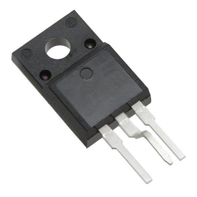
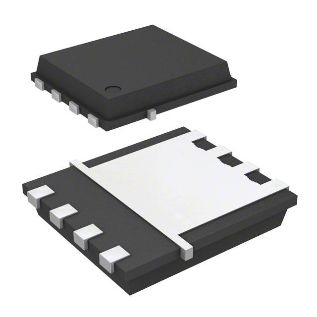
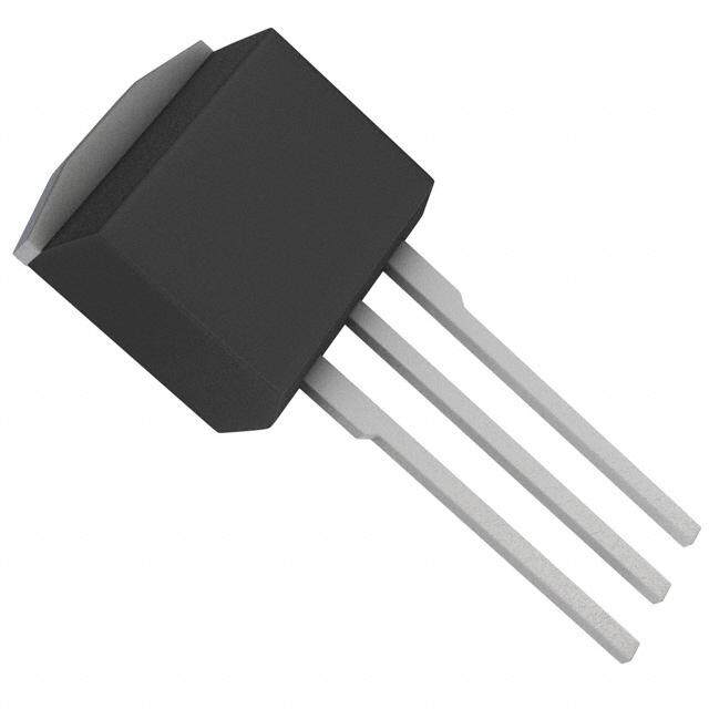
| 供应商器件封装 | I-Pak |
| 其它名称 | NTD5867NL-1G-ND |
| 功率-最大值 | 36W |
| 功率耗散 | 36 W |
| 包装 | 管件 |
| 商标 | ON Semiconductor |
| 安装类型 | 通孔 |
| 安装风格 | Through Hole |
| 导通电阻 | 39 mOhms |
| 封装/外壳 | TO-251-3 短引线,IPak,TO-251AA |
| 封装/箱体 | IPAK-3 |
| 工厂包装数量 | 75 |
| 晶体管极性 | N-Channel |
| 最大工作温度 | + 150 C |
| 最小工作温度 | - 55 C |
| 标准包装 | 75 |
| 汲极/源极击穿电压 | 60 V |
| 漏极连续电流 | 20 A |
| 漏源极电压(Vdss) | 60V |
| 电流-连续漏极(Id)(25°C时) | 20A (Tc) |
| 配置 | Single |
| 闸/源击穿电压 | +/- 20 V |


- 商务部:美国ITC正式对集成电路等产品启动337调查
- 曝三星4nm工艺存在良率问题 高通将骁龙8 Gen1或转产台积电
- 太阳诱电将投资9.5亿元在常州建新厂生产MLCC 预计2023年完工
- 英特尔发布欧洲新工厂建设计划 深化IDM 2.0 战略
- 台积电先进制程称霸业界 有大客户加持明年业绩稳了
- 达到5530亿美元!SIA预计今年全球半导体销售额将创下新高
- 英特尔拟将自动驾驶子公司Mobileye上市 估值或超500亿美元
- 三星加码芯片和SET,合并消费电子和移动部门,撤换高东真等 CEO
- 三星电子宣布重大人事变动 还合并消费电子和移动部门
- 海关总署:前11个月进口集成电路产品价值2.52万亿元 增长14.8%


PDF Datasheet 数据手册内容提取
NTD5867NL N-Channel Power MOSFET 60 V, 20 A, 39 m(cid:2) Features • Low R DS(on) • High Current Capability • http://onsemi.com 100% Avalanche Tested • These Devices are Pb−Free, Halogen Free/BFR Free and are RoHS V(BR)DSS RDS(on) MAX ID MAX Compliant 39 m(cid:4) @ 10 V 20 A 60 V MAXIMUM RATINGS (TJ = 25°C unless otherwise noted) 50 m(cid:4) @ 4.5 V 18 A Parameter Symbol Value Unit D Drain−to−Source Voltage VDSS 60 V Gate−to−Source Voltage − Continuous VGS ±20 V Gate−to−Source Voltage VGS ±30 V N−Channel − Non−Repetitive (tp < 10 (cid:2)s) G Continuous Drain TC = 25°C ID 20 A Current (R(cid:3)JC) Steady TC = 100°C 13 S Power Dissipation State TC = 25°C PD 36 W 4 (R(cid:3)JC) Pulsed Drain Current tp = 10 (cid:2)s IDM 76 A 4 Operating Junction and Storage Temperature TJ, Tstg −15550 to °C 1 2 12 3 3 Source Current (Body Diode) IS 20 A DPAK IPAK Single Pulse Drain−to−Source Avalanche EAS 18 mJ CASE 369AA CASE 369D Energy (VDD = 50 V, VGS = 10 V, RG = 25 (cid:4), (Surface Mount) (Straight Lead) IL(pk) = 19 A, L = 0.1 mH, TJ = 25°C) STYLE 2 STYLE 2 L(1e/a8d″ fTreommp cearsaetu froer f1o0r Ss)oldering Purposes TL 260 °C MARKING DIAGRAMS & PIN ASSIGNMENT Stresses exceeding those listed in the Maximum Ratings table may damage the device. If any of these limits are exceeded, device functionality should not be 4 Drain assumed, damage may occur and reliability may be affected. 4 W G THERMAL RESISTANCE MAXIMUM RATINGS Drain W NL Y87 Parameter Symbol Value Unit A56 W G Junction−to−Case (Drain) R(cid:3)JC 3.5 °C/W W NL Y87 Junction−to−Ambient − Steady State (Note 1) R(cid:3)JA 45 A56 1. Surface−mounted on FR4 board using 1 in sq pad size 2 (Cu area = 1.127 in sq [2 oz] including traces. 1Drain 3 1 2 3 Gate Source GateDrainSource A = Assembly Location* Y = Year WW = Work Week 5867NL= Device Code G = Pb−Free Package * The Assembly Location code (A) is front side optional. In cases where the Assembly Location is stamped in the package, the front side assembly code may be blank. ORDERING INFORMATION See detailed ordering and shipping information on page 5 of this data sheet. © Semiconductor Components Industries, LLC, 2014 1 Publication Order Number: September, 2014 − Rev. 3 NTD5867NL/D
NTD5867NL ELECTRICAL CHARACTERISTICS (TJ = 25°C unless otherwise noted) Parameter Symbol Test Condition Min Typ Max Unit OFF CHARACTERISTICS Drain−to−Source Breakdown Voltage V(BR)DSS VGS = 0 V, ID = 250 (cid:2)A 60 V Drain−to−Source Breakdown Voltage V(BR)DSS/TJ 60 mV/°C Temperature Coefficient Zero Gate Voltage Drain Current IDSS VGS = 0 V, TJ = 25°C 1.0 (cid:2)A VDS = 60 V TJ = 125°C 100 Gate−to−Source Leakage Current IGSS VDS = 0 V, VGS = ±20 V ±100 nA ON CHARACTERISTICS (Note 2) Gate Threshold Voltage VGS(TH) VGS = VDS, ID = 250 (cid:2)A 1.5 1.8 2.5 V Negative Threshold Temperature Coefficient VGS(TH)/TJ 5.2 mV/°C Drain−to−Source On Resistance RDS(on) VGS = 10 V, ID = 10 A 26 39 m(cid:4) VGS = 4.5 V, ID = 10 A 33 50 Forward Transconductance gFS VDS = 15 V, ID = 10 A 8.0 S CHARGES, CAPACITANCES AND GATE RESISTANCES Input Capacitance Ciss 675 pF Output Capacitance Coss VGS =V 0D VS, =f =2 51 .V0 MHz, 68 Reverse Transfer Capacitance Crss 47 Total Gate Charge QG(TOT) 15 nC Threshold Gate Charge QG(TH) VGS = 10 V, VDS = 48 V, 1.0 Gate−to−Source Charge QGS ID = 20 A 2.2 Gate−to−Drain Charge QGD 4.3 Total Gate Charge QG(TOT) VGS = 4.5 V, VDS = 48 V, 7.6 nC ID = 20 A Gate Resistance RG 1.3 (cid:4) SWITCHING CHARACTERISTICS (Note 3) Turn−On Delay Time td(on) 6.5 ns Rise Time tr VGS = 10 V, VDD = 48 V, 12.6 Turn−Off Delay Time td(off) ID = 20 A, RG = 2.5 (cid:4) 18.2 Fall Time tf 2.4 DRAIN−SOURCE DIODE CHARACTERISTICS Forward Diode Voltage VSD VGS = 0 V, TJ = 25°C 0.87 1.2 V IS = 10 A TJ = 100°C 0.78 Reverse Recovery Time tRR 17 ns Charge Time ta VGS = 0 V, dIs/dt = 100 A/(cid:2)s, 13 Discharge Time tb IS = 20 A 4.0 Reverse Recovery Charge QRR 12 nC Product parametric performance is indicated in the Electrical Characteristics for the listed test conditions, unless otherwise noted. Product performance may not be indicated by the Electrical Characteristics if operated under different conditions. 2. Pulse Test: Pulse Width ≤ 300 (cid:2)s, Duty Cycle ≤ 2%. 3. Switching characteristics are independent of operating junction temperatures. http://onsemi.com 2
NTD5867NL TYPICAL PERFORMANCE CURVES 40 40 10V 4.5 V TJ = 25°C VDS ≥ 10 V 35 35 S) 4 V S) P P M 30 M 30 A 3.8 V A T ( 25 T ( 25 N N E 3.6 V E R R R 20 R 20 U U C 3.4 V C AIN 15 3.2 V AIN 15 TJ = 125°C R 10 R 10 , DD 3.0 V , DD TJ = 25°C I 5 I 5 2.8 V TJ = −55°C 0 0 0 1 2 3 4 5 2 3 4 5 VDS, DRAIN−TO−SOURCE VOLTAGE (VOLTS) VGS, GATE−TO−SOURCE VOLTAGE (VOLTS) Figure 1. On−Region Characteristics Figure 2. Transfer Characteristics (cid:4)) (cid:4)) E (0.060 E ( 0.040 ANC ID = 20 A ANC TJ = 25°C ST TJ = 25°C ST ESI0.050 ESI 0.035 VGS = 4.5 V R R E E C C R R OU0.040 OU 0.030 S S − − TO TO VGS = 10 V − − N0.030 N 0.025 AI AI R R D D , DS(on)0.0203 4 5 6 7 8 9 10, DS(on)0.0205 10 15 20 R R VGS, GATE−TO−SOURCE VOLTAGE (VOLTS) ID, DRAIN CURRENT (AMPS) Figure 3. On−Resistance vs. Gate−to−Source Figure 4. On−Resistance vs. Drain Current and Voltage Gate Voltage 2.2 10000 E TANC 2.0 IVDG =S 2=0 1 A0 V VGS = 0 V ESIS 1.8 A) TJ = 150°C R n1000 N−TO−SOURCE (NORMALIZED) 1111....0246 I, LEAKAGE (DSS 100 TJ = 125°C AI R 0.8 D , on) 0.6 10 S( −50 −25 0 25 50 75 100 125 150 10 20 30 40 50 60 D R TJ, JUNCTION TEMPERATURE (°C) VDS, DRAIN−TO−SOURCE VOLTAGE (VOLTS) Figure 5. On−Resistance Variation with Figure 6. Drain−to−Source Leakage Current Temperature vs. Drain Voltage http://onsemi.com 3
NTD5867NL TYPICAL PERFORMANCE CURVES 1000 10 900 VTGJ S= =2 50° VC OLTS) QT 800 V 8 F) E ( CE (p 760000 Ciss LTAG 6 VGS N O A V APACIT 450000 URCE 4 Qgs Qgd C 300 O C, −S 120000 Coss E−TO 2 VIDD =S 2=0 4 A8 V Crss AT TJ = 25°C 0 G 0 0 10 20 30 40 50 60 , S 0 5 10 15 DRAIN−TO−SOURCE VOLTAGE (VOLTS) VG QG, TOTAL GATE CHARGE (nC) Figure 7. Capacitance Variation Figure 8. Gate−To−Source Voltage vs. Total Charge 1000 20 VDD = 48 V VGS = 0 V IVDG =S 2=0 1 A0 V MPS) TJ = 25°C A 15 100 T ( s) tf td(off) EN ME (n tr URR 10 t, TI 10 td(on) RCE C OU 5 S , S I 1 0 1 10 100 0.5 0.6 0.7 0.8 0.9 1.0 RG, GATE RESISTANCE (OHMS) VSD, SOURCE−TO−DRAIN VOLTAGE (VOLTS) Figure 9. Resistive Switching Time Figure 10. Diode Forward Voltage vs. Current Variation vs. Gate Resistance 100 20 E PS) 10 (cid:2)s URC ID = 20 A M O RRENT (A 10 110 m0 s(cid:2)s AIN−TO−SERGY (mJ) 15 U RN 10 N C VGS = 10 V 10 ms E DE E DRAI 1 STCIN =G 2L5E° CPULSE dc PULSNCH I, D RTHDSE(RonM) ALILM LITIMIT GLE VALA 5 NA PACKAGE LIMIT SI 0.11 10 100 S, 025 50 75 100 125 150 A VDS, DRAIN−TO−SOURCE VOLTAGE (VOLTS) E TJ, JUNCTION TEMPERATURE (°C) Figure 11. Maximum Rated Forward Biased Figure 12. Maximum Avalanche Energy vs. Safe Operating Area Starting Junction Temperature http://onsemi.com 4
NTD5867NL TYPICAL PERFORMANCE CURVES E C N TA 10 S SI E R L A THERMLIZED) 1.0 D = 0.5 NT MA 0.2 P(pk) SIENOR 0.1 00..015 RD (cid:3)CJCU(Rt) V=E rS(t )A RP(cid:3)PJCLY FOR POWER AN( 0.02 PULSE TRAIN SHOWN R T t1 READ TIME AT t1 VE 0.01 t2 TJ(pk) − TC = P(pk) R(cid:3)JC(t) TI SINGLE PULSE DUTY CYCLE, D = t1/t2 C 0.01 FE 0.000001 0.00001 0.0001 0.001 0.01 0.1 F E t, TIME (s) r(t), Figure 13. Thermal Response ORDERING INFORMATION Order Number Package Shipping† NTD5867NL−1G IPAK (Straight Lead) 75 Units / Rail (Pb−Free) NTD5867NLT4G DPAK 2500 / Tape & Reel (Pb−Free) †For information on tape and reel specifications, including part orientation and tape sizes, please refer to our Tape and Reel Packaging Specifications Brochure, BRD8011/D. http://onsemi.com 5
NTD5867NL PACKAGE DIMENSIONS DPAK (SINGLE GUAGE) CASE 369AA ISSUE B NOTES: C 1.DIMENSIONING AND TOLERANCING PER ASME A Y14.5M, 1994. E A 2.CONTROLLING DIMENSION: INCHES. 3.THERMAL PAD CONTOUR OPTIONAL WITHIN DI- MENSIONS b3, L3 and Z. b3 B c2 4.DIMENSIONS D AND E DO NOT INCLUDE MOLD FLASH, PROTRUSIONS, OR BURRS. MOLD FLASH, PROTRUSIONS, OR GATE BURRS SHALL NOT EXCEED 0.006 INCHES PER SIDE. L3 4 D Z 5.DOIUMTEENRSMIOONSST DE XATNRDE ME EASR EO FD ETTHEER PMLIANSETDIC A TB OTHDEY. H 6.DATUMS A AND B ARE DETERMINED AT DATUM 1 2 3 DETAIL A PLANE H. INCHES MILLIMETERS DIM MIN MAX MIN MAX L4 A 0.086 0.094 2.18 2.38 b2 A1 0.000 0.005 0.00 0.13 b c b 0.025 0.035 0.63 0.89 b2 0.030 0.045 0.76 1.14 e 0.005 (0.13) M C H b3 0.180 0.215 4.57 5.46 c 0.018 0.024 0.46 0.61 L2 GPLAAUNGEE C SPELAATNIENG cD2 00..203158 00..204254 50..9476 60..2621 E 0.250 0.265 6.35 6.73 e 0.090 BSC 2.29 BSC L H 0.370 0.410 9.40 10.41 A1 L 0.055 0.070 1.40 1.78 L1 L1 0.108 REF 2.74 REF L2 0.020 BSC 0.51 BSC DETAIL A L3 0.035 0.050 0.89 1.27 ROTATED 90(cid:2) CW L4 −−− 0.040 −−− 1.01 Z 0.155 −−− 3.93 −−− SOLDERING FOOTPRINT* STYLE 2: PIN 1. GATE 6.20 3.0 2. DRAIN 3. SOURCE 0.244 0.118 4. DRAIN 2.58 0.101 5.80 1.6 6.172 0.228 0.063 0.243 (cid:2) (cid:3) mm SCALE 3:1 inches *For additional information on our Pb−Free strategy and soldering details, please download the ON Semiconductor Soldering and Mounting Techniques Reference Manual, SOLDERRM/D. http://onsemi.com 6
NTD5867NL PACKAGE DIMENSIONS IPAK (STRAIGHT LEAD DPAK) CASE 369D ISSUE C B C NOTES: 1. DIMENSIONING AND TOLERANCING PER V R E ANSI Y14.5M, 1982. 2. CONTROLLING DIMENSION: INCH. INCHES MILLIMETERS 4 Z DIM MIN MAX MIN MAX A 0.235 0.245 5.97 6.35 A S B 0.250 0.265 6.35 6.73 1 2 3 C 0.086 0.094 2.19 2.38 D 0.027 0.035 0.69 0.88 E 0.018 0.023 0.46 0.58 −T− F 0.037 0.045 0.94 1.14 SEATING G 0.090 BSC 2.29 BSC PLANE K H 0.034 0.040 0.87 1.01 J 0.018 0.023 0.46 0.58 K 0.350 0.380 8.89 9.65 R 0.180 0.215 4.45 5.45 F J S 0.025 0.040 0.63 1.01 H V 0.035 0.050 0.89 1.27 Z 0.155 −−− 3.93 −−− D 3 PL STYLE 2: G 0.13 (0.005) M T PIN 1. GATE 2. DRAIN 3. SOURCE 4. DRAIN ON Semiconductor and the are registered trademarks of Semiconductor Components Industries, LLC (SCILLC) or its subsidiaries in the United States and/or other countries. SCILLC owns the rights to a number of patents, trademarks, copyrights, trade secrets, and other intellectual property. A listing of SCILLC’s product/patent coverage may be accessed at www.onsemi.com/site/pdf/Patent−Marking.pdf. SCILLC reserves the right to make changes without further notice to any products herein. SCILLC makes no warranty, representation or guarantee regarding the suitability of its products for any particular purpose, nor does SCILLC assume any liability arising out of the application or use of any product or circuit, and specifically disclaims any and all liability, including without limitation special, consequential or incidental damages. “Typical” parameters which may be provided in SCILLC data sheets and/or specifications can and do vary in different applications and actual performance may vary over time. All operating parameters, including “Typicals” must be validated for each customer application by customer’s technical experts. SCILLC does not convey any license under its patent rights nor the rights of others. SCILLC products are not designed, intended, or authorized for use as components in systems intended for surgical implant into the body, or other applications intended to support or sustain life, or for any other application in which the failure of the SCILLC product could create a situation where personal injury or death may occur. Should Buyer purchase or use SCILLC products for any such unintended or unauthorized application, Buyer shall indemnify and hold SCILLC and its officers, employees, subsidiaries, affiliates, and distributors harmless against all claims, costs, damages, and expenses, and reasonable attorney fees arising out of, directly or indirectly, any claim of personal injury or death associated with such unintended or unauthorized use, even if such claim alleges that SCILLC was negligent regarding the design or manufacture of the part. SCILLC is an Equal Opportunity/Affirmative Action Employer. This literature is subject to all applicable copyright laws and is not for resale in any manner. PUBLICATION ORDERING INFORMATION LITERATURE FULFILLMENT: N. American Technical Support: 800−282−9855 Toll Free ON Semiconductor Website: www.onsemi.com Literature Distribution Center for ON Semiconductor USA/Canada P.O. Box 5163, Denver, Colorado 80217 USA Europe, Middle East and Africa Technical Support: Order Literature: http://www.onsemi.com/orderlit Phone: 303−675−2175 or 800−344−3860 Toll Free USA/Canada Phone: 421 33 790 2910 Fax: 303−675−2176 or 800−344−3867 Toll Free USA/Canada Japan Customer Focus Center For additional information, please contact your local Email: orderlit@onsemi.com Phone: 81−3−5817−1050 Sales Representative http://onsemi.com NTD5867NL/D 7