ICGOO在线商城 > 分立半导体产品 > 晶体管 - FET,MOSFET - 单 > IRFPS37N50APBF
 Datasheet下载
- 型号: IRFPS37N50APBF
- 制造商: Vishay
- 库位|库存: xxxx|xxxx
- 要求:
| 数量阶梯 | 香港交货 | 国内含税 |
| +xxxx | $xxxx | ¥xxxx |
查看当月历史价格
查看今年历史价格
IRFPS37N50APBF产品简介:
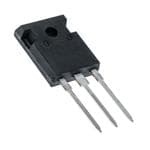
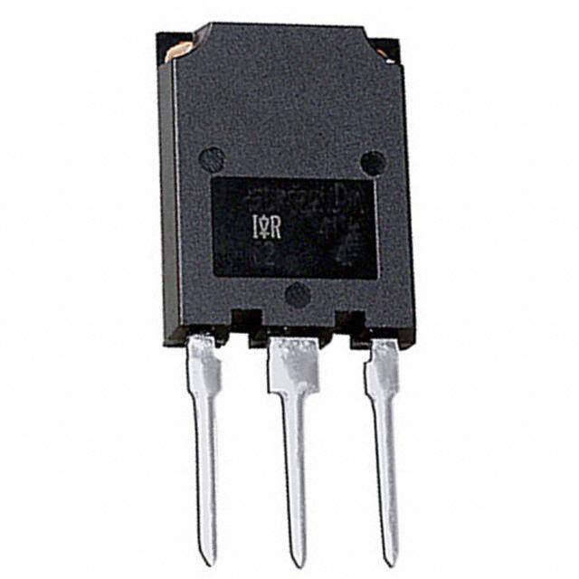
ICGOO电子元器件商城为您提供IRFPS37N50APBF由Vishay设计生产,在icgoo商城现货销售,并且可以通过原厂、代理商等渠道进行代购。 IRFPS37N50APBF价格参考。VishayIRFPS37N50APBF封装/规格:晶体管 - FET,MOSFET - 单, 通孔 N 沟道 500V 36A(Tc) 446W(Tc) SUPER-247(TO-274AA)。您可以下载IRFPS37N50APBF参考资料、Datasheet数据手册功能说明书,资料中有IRFPS37N50APBF 详细功能的应用电路图电压和使用方法及教程。
Vishay Siliconix的IRFPS37N50APBF是一款N沟道功率MOSFET,主要用于高电压、高电流的应用场景。该器件具有500V的击穿电压(BVdss),最大导通电阻为0.42Ω(在Vgs=10V时),适用于多种电力电子设备中。

 应用场景:

1. 开关电源 (SMPS):
   IRFPS37N50APBF广泛应用于开关电源中,特别是在需要高效能和高可靠性的场合。其低导通电阻和高击穿电压使其能够在高压环境下稳定工作,减少能量损耗,提高转换效率。

2. 电机驱动:
   在电机驱动应用中,这款MOSFET可以用于控制电机的启动、停止和调速。由于其快速开关特性和低导通电阻,能够有效减少发热,延长设备使用寿命。

3. 逆变器:
   逆变器是将直流电转换为交流电的设备,广泛应用于太阳能发电系统和不间断电源(UPS)中。IRFPS37N50APBF可以在这些系统中作为关键的开关元件,确保高效的电力转换。

4. 工业自动化:
   在工业自动化领域,该MOSFET可用于各种控制电路中,如PLC(可编程逻辑控制器)和伺服驱动器。其高可靠性有助于提高整个系统的稳定性。

5. 电动汽车 (EV) 和混合动力汽车 (HEV):
   在电动汽车和混合动力汽车的动力管理系统中,IRFPS37N50APBF可以用于电池管理和电机驱动电路,确保车辆在高压环境下安全运行。

6. LED驱动器:
   在大功率LED照明系统中,这款MOSFET可以用作电流调节器或开关元件,确保LED灯的稳定性和长寿命。

7. 光伏系统:
   在太阳能光伏系统中,IRFPS37N50APBF可以用于DC-DC转换器和MPPT(最大功率点跟踪)控制器,以优化太阳能电池板的能量输出。

总之,IRFPS37N50APBF凭借其优异的电气特性,适用于多种高电压、大电流的电力电子应用,尤其适合对效率和可靠性要求较高的场合。
| 参数 | 数值 |
| 产品目录 | |
| ChannelMode | Enhancement |
| 描述 | MOSFET N-CH 500V 36A SUPER247MOSFET N-Chan 500V 36 Amp |
| 产品分类 | FET - 单分离式半导体 |
| FET功能 | 标准 |
| FET类型 | MOSFET N 通道,金属氧化物 |
| Id-ContinuousDrainCurrent | 36 A |
| Id-连续漏极电流 | 36 A |
| 品牌 | Vishay / SiliconixVishay Siliconix |
| 产品手册 | |
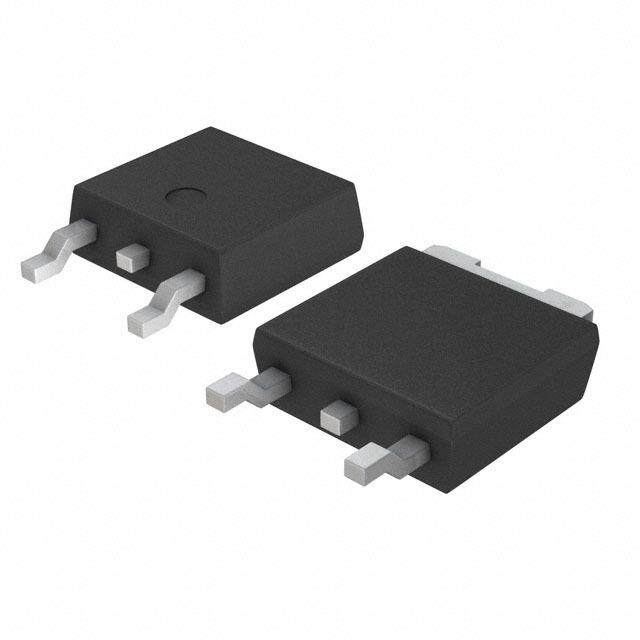
| 产品图片 |
|
| rohs | RoHS 合规性豁免无铅 / 符合限制有害物质指令(RoHS)规范要求 |
| 产品系列 | 晶体管,MOSFET,Vishay / Siliconix IRFPS37N50APBF- |
| 数据手册 | |
| 产品型号 | IRFPS37N50APBFIRFPS37N50APBF |
| Pd-PowerDissipation | 446 W |
| Pd-功率耗散 | 446 W |
| RdsOn-Drain-SourceResistance | 130 mOhms |
| RdsOn-漏源导通电阻 | 130 mOhms |
| Vds-Drain-SourceBreakdownVoltage | 500 V |
| Vds-漏源极击穿电压 | 500 V |
| Vgs-Gate-SourceBreakdownVoltage | +/- 30 V |
| Vgs-栅源极击穿电压 | 30 V |
| 上升时间 | 98 ns |
| 下降时间 | 80 ns |
| 不同Id时的Vgs(th)(最大值) | 4V @ 250µA |
| 不同Vds时的输入电容(Ciss) | 5579pF @ 25V |
| 不同Vgs时的栅极电荷(Qg) | 180nC @ 10V |
| 不同 Id、Vgs时的 RdsOn(最大值) | 130 毫欧 @ 22A,10V |
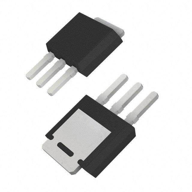
| 产品目录绘图 |
|
| 产品目录页面 | |
| 产品种类 | MOSFET |
| 供应商器件封装 | SUPER-247(TO-274AA) |
| 其它名称 | *IRFPS37N50APBF |
| 典型关闭延迟时间 | 52 ns |
| 功率-最大值 | 446W |
| 功率耗散 | 446 W |
| 包装 | 管件 |
| 商标 | Vishay / Siliconix |
| 安装类型 | 通孔 |
| 安装风格 | Through Hole |
| 导通电阻 | 130 mOhms |
| 封装 | Tube |
| 封装/外壳 | TO-274AA |
| 封装/箱体 | Super247-3 |
| 工厂包装数量 | 500 |
| 晶体管极性 | N-Channel |
| 最大工作温度 | + 150 C |
| 最小工作温度 | - 55 C |
| 标准包装 | 25 |
| 汲极/源极击穿电压 | 500 V |
| 漏极连续电流 | 36 A |
| 漏源极电压(Vdss) | 500V |
| 电流-连续漏极(Id)(25°C时) | 36A (Tc) |
| 通道模式 | Enhancement |
| 配置 | Single |
| 闸/源击穿电压 | +/- 30 V |


- 商务部:美国ITC正式对集成电路等产品启动337调查
- 曝三星4nm工艺存在良率问题 高通将骁龙8 Gen1或转产台积电
- 太阳诱电将投资9.5亿元在常州建新厂生产MLCC 预计2023年完工
- 英特尔发布欧洲新工厂建设计划 深化IDM 2.0 战略
- 台积电先进制程称霸业界 有大客户加持明年业绩稳了
- 达到5530亿美元!SIA预计今年全球半导体销售额将创下新高
- 英特尔拟将自动驾驶子公司Mobileye上市 估值或超500亿美元
- 三星加码芯片和SET,合并消费电子和移动部门,撤换高东真等 CEO
- 三星电子宣布重大人事变动 还合并消费电子和移动部门
- 海关总署:前11个月进口集成电路产品价值2.52万亿元 增长14.8%


PDF Datasheet 数据手册内容提取
PD- 91822C IRFPS37N50A SMPS MOSFET HEXFET® Power MOSFET Applications V R max I l Switch Mode Power Supply (SMPS) DSS DS(on) D l Uninterruptable Power Supply 500V 0.13W 36A l High Speed Power Switching Benefits l Low Gate Charge Qg results in Simple Drive Requirement l Improved Gate, Avalanche and Dynamic dv/dt Ruggedness l Fully Characterized Capacitance and Avalanche Voltage and Current SUPER-247 l Effective Coss Specified (See AN 1001) Absolute Maximum Ratings Parameter Max. Units I @ T = 25°C Continuous Drain Current, V @ 10V 36 D C GS I @ T = 100°C Continuous Drain Current, V @ 10V 23 A D C GS I Pulsed Drain Current (cid:129) 144 DM P @T = 25°C Power Dissipation 446 W D C Linear Derating Factor 3.6 W/°C V Gate-to-Source Voltage ± 30 V GS dv/dt Peak Diode Recovery dv/dt (cid:131) 3.5 V/ns T Operating Junction and -55 to + 150 J TSTG Storage Temperature Range °C Soldering Temperature, for 10 seconds 300 (1.6mm from case ) Typical SMPS Topologies l Full Bridge Converters l Power Factor Correction Boost Notes (cid:129) through (cid:133) are on page 8 www.irf.com 1 12/14/99
IRFPS37N50A Static @ T = 25°C (unless otherwise specified) J Parameter Min. Typ. Max. Units Conditions V(BR)DSS Drain-to-Source Breakdown Voltage 500 ––– ––– V VGS = 0V, ID = 250µA RDS(on) Static Drain-to-Source On-Resistance ––– ––– 0.13 W VGS = 10V, ID = 22A (cid:132) VGS(th) Gate Threshold Voltage 2.0 ––– 4.0 V VDS = VGS, ID = 250µA IDSS Drain-to-Source Leakage Current ––– ––– 25 µA VDS = 500V, VGS = 0V ––– ––– 250 VDS = 400V, VGS = 0V, TJ = 150°C I Gate-to-Source Forward Leakage ––– ––– 100 nA VGS = 30V GSS Gate-to-Source Reverse Leakage ––– ––– -100 VGS = -30V Dynamic @ T = 25°C (unless otherwise specified) J Parameter Min. Typ. Max. Units Conditions gfs Forward Transconductance 20 ––– ––– S VDS = 50V, ID = 22A Qg Total Gate Charge ––– ––– 180 ID = 36A Qgs Gate-to-Source Charge ––– ––– 46 nC VDS = 400V Qgd Gate-to-Drain ("Miller") Charge ––– ––– 71 VGS = 10V, See Fig. 6 and 13 (cid:132) td(on) Turn-On Delay Time ––– 23 ––– VDD = 250V tr Rise Time ––– 98 ––– ns ID = 36A td(off) Turn-Off Delay Time ––– 52 ––– RG = 2.15W tf Fall Time ––– 80 ––– RD = 7.0W ,See Fig. 10 (cid:132) Ciss Input Capacitance ––– 5579 ––– VGS = 0V Coss Output Capacitance ––– 810 ––– VDS = 25V Crss Reverse Transfer Capacitance ––– 36 ––– pF ƒ = 1.0MHz, See Fig. 5 Coss Output Capacitance ––– 7905 ––– VGS = 0V, VDS = 1.0V, ƒ = 1.0MHz Coss Output Capacitance ––– 221 ––– VGS = 0V, VDS = 400V, ƒ = 1.0MHz Coss eff. Effective Output Capacitance ––– 400 ––– VGS = 0V, VDS = 0V to 400V (cid:133) Avalanche Characteristics Parameter Typ. Max. Units E Single Pulse Avalanche Energy(cid:130) ––– 1260 mJ AS I Avalanche Current(cid:129) ––– 36 A AR E Repetitive Avalanche Energy(cid:129) ––– 44 mJ AR Thermal Resistance Parameter Typ. Max. Units Rq JC Junction-to-Case ––– 0.28 Rq CS Case-to-Sink, Flat, Greased Surface 0.24 ––– °C/W Rq JA Junction-to-Ambient ––– 40 Diode Characteristics Parameter Min. Typ. Max. Units Conditions IS Continuous Source Current ––– ––– 36 MOSFET symbol D (Body Diode) showing the A ISM Pulsed Source Current ––– ––– 144 integral reverse G (Body Diode) (cid:129) p-n junction diode. S VSD Diode Forward Voltage ––– ––– 1.5 V TJ = 25°C, IS = 36A, VGS = 0V (cid:132) trr Reverse Recovery Time ––– 570 860 ns TJ = 25°C, IF = 36A Qrr Reverse RecoveryCharge ––– 8.6 13 µC di/dt = 100A/µs (cid:132) ton Forward Turn-On Time Intrinsic turn-on time is negligible (turn-on is dominated by LS+LD) 2 www.irf.com
IRFPS37N50A 1000 100 VGS VGS TOP 15V TOP 15V 10V 10V A) 87..00VV A) 87..00VV urrent ( 100 BOTTOM6554....0505VVVV urrent ( BOTTOM6554....0505VVVV C C e e c c our 10 our 10 S S o- o- 4.5V n-t n-t ai ai Dr 4.5V Dr I , D 1 I , D 20µs PULSE WIDTH 20µs PULSE WIDTH TJ = 25°C TJ = 150°C 0.1 1 0.1 1 10 100 0.1 1 10 100 VD S , Drain-to-Source Voltage (V) V D S , Drain-to-Source Voltage (V) Fig 1. Typical Output Characteristics Fig 2. Typical Output Characteristics 1000 3.0 ID=36A e c A) an 2.5 ent ( esist Source Curr 100 TJ = 150 ° C ource On Rmalized) 12..50 I , Drain-to-D 10 TJ = 25 ° CV20 D µ Ss =P U50LVSE WIDTH R , Drain-to-SDS(on)(Nor 01..50 VGS=10V 1 0.0 4.0 5.0 6.0 7.0 8.0 9.0 -60 -40 -20 0 20 40 60 80 100 120 140 160 VG S , Gate-to-Source Voltage (V) TJ , Junction Temperature ( ° C) Fig 3. Typical Transfer Characteristics Fig 4. Normalized On-Resistance Vs. Temperature www.irf.com 3
IRFPS37N50A 100000 20 V G S = 0V, f = 1MHz ID=36A C is s = C g s + C g d , C d s SHORTED 10000 CC or s ss s == CC dg s d + C gd ge (V) 16 VVVDDDSSS=== 124050000VVV ) a pF Ci ss olt ce ( e V 12 n c a ur Capacit 1000 C oss e-to-So 8 C, at G 100 Cr ss V , GS 4 FOR TEST CIRCUIT SEE FIGURE 1 3 10 A 0 1 10 100 1000 0 40 80 120 160 200 V D S , Drain-to-Source Voltage (V) Q G , Total Gate Charge (nC) Fig 5. Typical Capacitance Vs. Fig 6. Typical Gate Charge Vs. Drain-to-Source Voltage Gate-to-Source Voltage 1000 1000 OPERATION IN THIS AREA LIMITED BY R DS(on) A) nt ( 100 e A)A) Curr nt (nt ( 100 10us ain TJ = 150 ° C urreurre se Dr 10 ain Cain C 100us I , ReverSD 1 TJ = 25 ° C I , DrI , DrD 10 TC= 25 ° C 110mmss T = 150 ° C J V G S = 0 V Single Pulse 0.1 1 0.2 0.4 0.6 0.8 1.0 1.2 1.4 10 100 1000 10000 VS D ,Source-to-Drain Voltage (V) VD S , Drain-to-Source Voltage (V) Fig 7. Typical Source-Drain Diode Fig 8. Maximum Safe Operating Area Forward Voltage 4 www.irf.com
IRFPS37N50A R 40 D V DS V GS D.U.T. R A) 30 G +-VDD nt ( e 10V Curr 20 Pulse Width £ 1 µs n Duty Factor £ 0.1 % ai Dr I , D 10 Fig 10a. Switching Time Test Circuit VDS 90% 0 25 50 75 100 125 150 T , Case Temperature ( ° C) C 10% VGS Fig 9. Maximum Drain Current Vs. td(on) tr td(off) tf Case Temperature Fig 10b. Switching Time Waveforms 1 ) Z thJC D = 0.50 ( 0.1 e 0.20 s n po 0.10 s ermal Re0.01 000...000125 SINGLE PULSE PDM t1 h (THERMAL RESPONSE) t2 T Notes: 1. Duty factor D = t 1 / t 2 2. Peak TJ=PDMx ZthJC + TC 0.001 0.00001 0.0001 0.001 0.01 0.1 1 t1 , Rectangular Pulse Duration (sec) Fig 11. Maximum Effective Transient Thermal Impedance, Junction-to-Case www.irf.com 5
IRFPS37N50A 3000 15V ID J) TOP 16A m VDS L DRIVER ergy (2500 BOTTOM 2336AA n E e 2000 RG D.U.T + ch IAS - VDDA alan1500 20V v tp 0.01W e A s Fig 12a. Unclamped Inductive Test Circuit ul1000 P V(BR)DSS gle n tp Si 500 E , AS 0 25 50 75 100 125 150 Starting T , Junction Temperature ( ° C) J IAS Fig 12c. Maximum Avalanche Energy Fig 12b. Unclamped Inductive Waveforms Vs. Drain Current Q G 10 V Q Q 580 GS GD ) V VG e ( g 560 a olt V Charge e h c Fig 13a. Basic Gate Charge Waveform an 540 al CurrentRegulator Av 12V Sam.2emFType50aKsW D.U.T. V , DSav 520 .3mF + D.U.T. -VDS 500 A 0 10 20 30 40 VGS I , Avalanche Current (A) av 3mA IG ID Fig 12d. Typical Drain-to-Source Voltage CurrentSamplingResistors Fig 13b. Gate Charge Test Circuit Vs. Avalanche Current 6 www.irf.com
IRFPS37N50A Peak Diode Recovery dv/dt Test Circuit + Circuit Layout Considerations D.U.T • Low Stray Inductance (cid:131) • Ground Plane • Low Leakage Inductance Current Transformer - + (cid:130) (cid:132) - + - (cid:129) RG • dv/dt controlled by RG + • Driver same type as D.U.T. V - DD • I controlled by Duty Factor "D" SD • D.U.T. - Device Under Test Driver Gate Drive P.W. Period D = P.W. Period V =10V * GS D.U.T. I Waveform SD Reverse Recovery Body Diode Forward Current Current di/dt D.U.T. V Waveform DS Diode Recovery dv/dt V DD Re-Applied Voltage Body Diode Forward Drop Inductor Curent Ripple £ 5% ISD * V = 5V for Logic Level Devices GS Fig 14. For N-channel HEXFET® Power MOSFETs www.irf.com 7
IRFPS37N50A Case Outline and Dimensions — Super-247 Dimensions are shown in millimeters Notes: (cid:129) Repetitive rating; pulse width limited by (cid:132) Pulse width £ 300µs; duty cycle £ 2%. max. junction temperature. ( See fig. 11 ) (cid:130) Starting T = 25°C, L = 1.94mH (cid:133) Coss eff. is a fixed capacitance that gives the same charging time J R = 25W , I = 36A. (See Figure 12) as Coss while VDS is rising from 0 to 80% VDSS G AS (cid:131)I £ 36A, di/dt £ 145A/µs, V £ V , SD DD (BR)DSS T £ 150°C J ** When mounted on 1" square PCB (FR-4 or G-10 Material ) . For recommended footprint and soldering techniques refer to application note #AN-994 WORLD HEADQUARTERS: 233 Kansas St., El Segundo, California 90245, Tel: (310) 252-7105 IR GREAT BRITAIN: Hurst Green, Oxted, Surrey RH8 9BB, UK Tel: ++ 44 1883 732020 IR CANADA: 15 Lincoln Court, Brampton, Ontario L6T3Z2, Tel: (905) 453 2200 IR GERMANY: Saalburgstrasse 157, 61350 Bad Homburg Tel: ++ 49 6172 96590 IR ITALY: Via Liguria 49, 10071 Borgaro, Torino Tel: ++ 39 11 451 0111 IR JAPAN: K&H Bldg., 2F, 30-4 Nishi-Ikebukuro 3-Chome, Toshima-Ku, Tokyo Japan 171 Tel: 81 3 3983 0086 IR SOUTHEAST ASIA: 1 Kim Seng Promenade, Great World City West Tower, 13-11, Singapore 237994 Tel: ++ 65 838 4630 IR TAIWAN:16 Fl. Suite D. 207, Sec. 2, Tun Haw South Road, Taipei, 10673, Taiwan Tel: 886-2-2377-9936 Data and specifications subject to change without notice. 12/99 8 www.irf.com
Mouser Electronics Authorized Distributor Click to View Pricing, Inventory, Delivery & Lifecycle Information: I nfineon: IRFPS37N50APBF