ICGOO在线商城 > 分立半导体产品 > 晶体管 - FET,MOSFET - 单 > STV300NH02L
 Datasheet下载
- 型号: STV300NH02L
- 制造商: STMicroelectronics
- 库位|库存: xxxx|xxxx
- 要求:
| 数量阶梯 | 香港交货 | 国内含税 |
| +xxxx | $xxxx | ¥xxxx |
查看当月历史价格
查看今年历史价格
STV300NH02L产品简介:
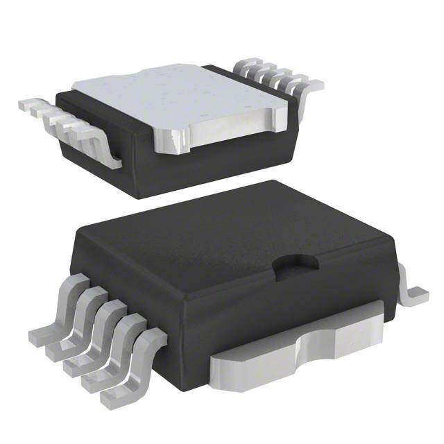
ICGOO电子元器件商城为您提供STV300NH02L由STMicroelectronics设计生产,在icgoo商城现货销售,并且可以通过原厂、代理商等渠道进行代购。 STV300NH02L价格参考。STMicroelectronicsSTV300NH02L封装/规格:晶体管 - FET,MOSFET - 单, 表面贴装 N 沟道 24V 200A(Tc) 300W(Tc) 10-PowerSO。您可以下载STV300NH02L参考资料、Datasheet数据手册功能说明书,资料中有STV300NH02L 详细功能的应用电路图电压和使用方法及教程。
STMicroelectronics(意法半导体)的STV300NH02L是一款N沟道增强型MOSFET,属于晶体管中的场效应管(FET)类别。该器件常用于需要高效功率控制的应用场景。

应用场景包括:

1. 电源管理:适用于DC-DC转换器、开关电源(SMPS)等,因其低导通电阻和高效能,有助于提高电源转换效率并减少发热。

2. 电机控制:在电动工具、电动车或工业自动化中用于控制直流电机的启停与转速,具备良好的负载能力和开关特性。

3. 负载开关:作为高边或低边开关用于控制大电流负载,如LED照明、加热元件或风扇等。

4. 电池供电设备:用于笔记本电脑、平板、UPS(不间断电源)等设备中,实现高效的电池充放电管理与功率控制。

5. 汽车电子:可用于车载电源系统、车身控制模块(如车窗、座椅调节)等对可靠性和效率要求较高的场景。

该MOSFET采用节能设计,具备较强的热稳定性和耐用性,适合在中高功率应用中替代传统晶体管,提升系统整体能效和可靠性。
| 参数 | 数值 |
| 产品目录 | |
| ChannelMode | Enhancement |
| 描述 | MOSFET N-CH 24V 280A POWERSO-10MOSFET N Ch 24V 0.8m 280A Pwr MOSFET |
| 产品分类 | FET - 单分离式半导体 |
| FET功能 | 标准 |
| FET类型 | MOSFET N 通道,金属氧化物 |
| Id-ContinuousDrainCurrent | 280 A |
| Id-连续漏极电流 | 280 A |
| 品牌 | STMicroelectronics |
| 产品手册 | |
| 产品图片 |
|
| rohs | 符合RoHS无铅 / 符合限制有害物质指令(RoHS)规范要求 |
| 产品系列 | 晶体管,MOSFET,STMicroelectronics STV300NH02LSTripFET™ III |
| 数据手册 | |
| 产品型号 | STV300NH02L |
| Pd-PowerDissipation | 300 W |
| Pd-功率耗散 | 300 W |
| RdsOn-Drain-SourceResistance | 1 mOhms |
| RdsOn-漏源导通电阻 | 1 mOhms |
| Vds-Drain-SourceBreakdownVoltage | 24 V |
| Vds-漏源极击穿电压 | 24 V |
| Vgs-Gate-SourceBreakdownVoltage | +/- 20 V |
| Vgs-栅源极击穿电压 | 20 V |
| 上升时间 | 275 ns |
| 下降时间 | 94.4 ns |
| 不同Id时的Vgs(th)(最大值) | 2V @ 250µA |
| 不同Vds时的输入电容(Ciss) | 7055pF @ 15V |
| 不同Vgs时的栅极电荷(Qg) | 109nC @ 10V |
| 不同 Id、Vgs时的 RdsOn(最大值) | 1 毫欧 @ 80A,10V |
| 产品培训模块 | http://www.digikey.cn/PTM/IndividualPTM.page?site=cn&lang=zhs&ptm=26067 |
| 产品目录页面 | |
| 产品种类 | MOSFET |
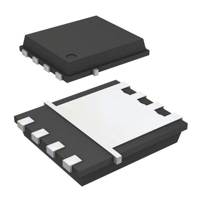
| 供应商器件封装 | 10-PowerSO |
| 其它名称 | 497-7614-6 |
| 其它有关文件 | http://www.st.com/web/catalog/sense_power/FM100/CL824/SC1164/PF167036?referrer=70071840 |
| 典型关闭延迟时间 | 138 ns |
| 功率-最大值 | 300W |
| 包装 | Digi-Reel® |
| 商标 | STMicroelectronics |
| 安装类型 | 表面贴装 |
| 安装风格 | SMD/SMT |
| 封装 | Reel |
| 封装/外壳 | PowerSO-10 裸露底部焊盘 |
| 封装/箱体 | PowerSO-12 |
| 工厂包装数量 | 600 |
| 晶体管极性 | N-Channel |
| 最大工作温度 | + 175 C |
| 最小工作温度 | - 55 C |
| 标准包装 | 1 |
| 漏源极电压(Vdss) | 24V |
| 特色产品 | http://www.digikey.com/cn/zh/ph/ST/PowerSO.html |
| 电流-连续漏极(Id)(25°C时) | 200A (Tc) |
| 系列 | STV300NH02L |
| 通道模式 | Enhancement |
| 配置 | Single |


PDF Datasheet 数据手册内容提取
STV300NH02L Ω N-channel 24 V, 0.8 m typ., 200 A STripFET™ III Power MOSFET in a PowerSO-10 package Datasheet — production data Features Order code V R max I DSS DS(on) D STV300NH02L 24 V 0.001 Ω 200 A(1) 10 1. This value is limited by package 1 ■ RDS(on)*Qg industry’s benchmark PowerSO-10 ■ Conduction losses reduced ■ Low profile, very low parasitic inductance ■ Switching losses reduced Applications Figure 1. Internal schematic diagram ■ Switching applications – OR-ing ■ Specially designed and optimized for high efficiency DC/DC converters. Description This N-channel enhancement mode Power MOSFET benefits from the latest refinement of STMicroelectronics’ unique “single feature size” strip-based process, which decreases the critical Figure 2. Connection diagram (top view) alignment steps to offer exceptional manufacturing reproducibility. The result is a transistor with extremely high packing density for low on-resistance, rugged avalanche characteristics and low gate charge. Table 1. Device summary Order code Marking Package Packaging STV300NH02L 300NH02L PowerSO-10 Tape and reel October 2012 Doc ID 13301 Rev 3 1/14 This is information on a product in full production. www.st.com 14
Content STV300NH02L Content 1 Electrical ratings . . . . . . . . . . . . . . . . . . . . . . . . . . . . . . . . . . . . . . . . . . . . 3 2 Electrical characteristics . . . . . . . . . . . . . . . . . . . . . . . . . . . . . . . . . . . . . 4 2.1 Electrical characteristics (curves) . . . . . . . . . . . . . . . . . . . . . . . . . . . . . 6 3 Test circuits . . . . . . . . . . . . . . . . . . . . . . . . . . . . . . . . . . . . . . . . . . . . . . 8 4 Package mechanical data . . . . . . . . . . . . . . . . . . . . . . . . . . . . . . . . . . . . . 9 5 Packaging mechanical data . . . . . . . . . . . . . . . . . . . . . . . . . . . . . . . . . . 11 6 Revision history . . . . . . . . . . . . . . . . . . . . . . . . . . . . . . . . . . . . . . . . . . . 13 2/14 Doc ID 13301 Rev 3
STV300NH02L Electrical ratings 1 Electrical ratings Table 2. Absolute maximum ratings Symbol Parameter Value Unit VDS Drain-source voltage 24 V VGS Gate-source voltage ± 20 V ID (1) Drain current (continuous) at TC = 25 °C 200 A ID (1) Drain current (continuous) at TC = 100 °C 200 A I (2) Drain current (pulsed) 800 A DM PTOT (3) Total dissipation at TC = 25°C 300 W Derating factor 2 W/°C E (4) Single pulse avalanche energy 1.6 J AS Tstg Storage temperature -55 to 175 °C Tj Operating junction temperature 1. This value is limited by package 2. Pulse with limited by safe operating area 3. This value is rated according to Rthj-c 4. Starting Tj = 25°C, I = 60A, V = 20V D DD Table 3. Thermal data Symbol Parameter Value Unit Rthj-case Thermal resistance junction-case max 0.5 °C/W Rthj-pcb (1) Thermal resistance junction-pcb max 35 °C/W 1. When mounted on 1 inch2 FR-4, 2 oz Cu Doc ID 13301 Rev 3 3/14
Electrical characteristics STV300NH02L 2 Electrical characteristics (Tcase =25°C unless otherwise specified) Table 4. On /off states Symbol Parameter Test conditions Min. Typ. Max. Unit Drain-source V(BR)DSS breakdown voltage ID = 1 mA 24 V (V = 0) GS Zero gate voltage drain VDS = 24 V 1 µA I DSS current (VGS = 0) VDS = 24 V, Tc=125 °C 10 µA Gate body leakage IGSS current (V = 0) VDS = ± 20 V ±100 nA DS VGS(th) Gate threshold voltage VDS= VGS, ID = 250 μA 1 1.5 2.5 V RDS(on) Sretsaitsicta dnrcaein-source on- VVGS== 150 V ,V ,I DI== 4 080 A A 10..185 11.5 mΩ GS D Table 5. Dynamic Symbol Parameter Test conditions Min. Typ. Max. Unit Ciss Input capacitance 7055 pF Output capacitance Coss VDS = 15V, f = 1 MHz, VGS =0 - 3251 - pF Reverse transfer C 307 pF rss capacitance Qg Total gate charge VDD= 12V, ID= 120A, 109 nC Qgs Gate-source charge VGS= 10V - 30 - nC Qgd Gate-drain charge (see Figure 15) 26 nC RG Gate input resistance VDS = 0V, f = 1 MHz, VGS =0 - 4.4 - Ω Table 6. Switching times Symbol Parameter Test conditions Min. Typ. Max Unit V = 12V, I = 60A td(on) Turn-on delay time RDD= 4.7Ω, VD = 10V, - 18 - ns t Rise time G GS 275 ns r (see Figure 14) V = 12V, I = 60A td(off) Turn-off delay time RDD= 4.7Ω, VD = 10V, - 138 - ns t Fall time G GS 94.4 ns f (see Figure 14) 4/14 Doc ID 13301 Rev 3
STV300NH02L Electrical characteristics Table 7. Source drain diode Symbol Parameter Test conditions Min. Typ. Max. Unit ISD Source-drain current 200 A - I Source-drain current (pulsed) 800 A SDM VSD (1) Forward on voltage ISD = 120A, VGS = 0 - 1.3 V trr Reverse recovery time ISD = 120A, di/dt = 100A/µs 63 ns Qrr Reverse recovery charge VDD = 20V, Tj = 25°C - 85 nC IRRM Reverse recovery current (see Figure 19) 2.7 A trr Reverse recovery time ISD = 120A, di/dt = 100A/µs 63 ns Qrr Reverse recovery charge VDD = 20V, Tj = 150°C - 88 nC IRRM Reverse recovery current (see Figure 19) 2.8 A 1. Pulsed: Pulse duration = 300 µs, duty cycle 1.5% Doc ID 13301 Rev 3 5/14
Electrical characteristics STV300NH02L 2.1 Electrical characteristics (curves) Figure 3. Safe operating area Figure 4. Thermal impedance ID AM14955v1 K Zth_PowerSO-10 1(0A0) OpLiermaittieodn ibny thmisa x arReDa Si(son) 100µs δ0=.20.5 0.1 1ms 10-1 0.05 10 0.02 10ms 0.01 Tj=175°C 10-2 1 Tc=25°C Single pulse Single pulse 0.1 10-3 0.1 1 10 VDS(V) 10-5 10-4 10-3 10-2 10-1 tp(s) Figure 5. Output characteristics Figure 6. Transfer characteristics Figure 7. Static drain-source on-resistance Figure 8. Normalized BV vs temperature DSS 6/14 Doc ID 13301 Rev 3
STV300NH02L Electrical characteristics Figure 9. Gate charge vs gate-source voltage Figure 10. Capacitance variations Figure 11. Normalized gate threshold voltage Figure 12. Normalized on-resistance vs vs temperature temperature Figure 13. Source-drain diode forward characteristics Doc ID 13301 Rev 3 7/14
Test circuits STV300NH02L 3 Test circuits Figure 14. Switching times test circuit for Figure 15. Gate charge test circuit resistive load VDD 12V 47kΩ 1kΩ 100nF RL 2μ20F0 3μ.F3 VDD IG=CONST VD Vi=20V=VGMAX 100Ω D.U.T. VGS 2200 RG D.U.T. μF 2.7kΩ VG PW 47kΩ 1kΩ PW AM01468v1 AM01469v1 Figure 16. Test circuit for inductive load Figure 17. Unclamped inductive load test switching and diode recovery times circuit L A A A D FAST L=100μH VD G D.U.T. DIODE 2200 3.3 μF μF VDD S B 3.3 1000 B B μF μF 25Ω D VDD ID G RG S Vi D.U.T. Pw AM01470v1 AM01471v1 Figure 18. Unclamped inductive waveform Figure 19. Switching time waveform V(BR)DSS ton toff VD tdon tr tdoff tf 90% 90% IDM 10% ID 0 10% VDS VDD VDD 90% VGS AM01472v1 0 10% AM01473v1 8/14 Doc ID 13301 Rev 3
STV300NH02L Package mechanical data 4 Package mechanical data In order to meet environmental requirements, ST offers these devices in different grades of ECOPACK® packages, depending on their level of environmental compliance. ECOPACK® specifications, grade definitions and product status are available at: www.st.com. ECOPACK is an ST trademark. Table 8. PowerSO-10 mechanical data mm Dim. Min. Typ. Max. A 3.70 A1 0.00 0.10 A2 3.40 3.60 A3 1.25 1.35 b 0.40 0.53 c 0.35 0.55 D 9.40 9.60 D1 7.40 7.60 E 13.80 14.40 E1 9.30 9.50 E2 7.20 7.60 E3 5.90 6.10 e 1.27 L 0.95 1.65 < 0o 8o Doc ID 13301 Rev 3 9/14
Package mechanical data STV300NH02L Figure 20. PowerSO-10 drawing 0068039F1_Rev.E 10/14 Doc ID 13301 Rev 3
STV300NH02L Packaging mechanical data 5 Packaging mechanical data Table 9. Carrier tape dimensions mm Ref. Min. Typ. Max. A0 14.9 15.0 15.1 B0 9.9 10.0 10.1 K0 4.15 4.25 4.35 F 11.4 11.5 11.6 E 1.65 1.75 1.85 W 23.7 24.0 24.3 P2 1.9 2.0 2.1 P0 3.9 4.0 4.1 P1 23.9 24.0 24.1 T 0.025 0.30 0.35 D(Ø) 1.50 1.55 1.60 Note: 10 sprocket hole pitch cumulative tolerance ±0.2 mm. Figure 21. Carrier tape drawing (a) (cid:33)(cid:45)(cid:16)(cid:22)(cid:16)(cid:19)(cid:23)(cid:86)(cid:17) a. Drawing is not to scale. Doc ID 13301 Rev 3 11/14
Packaging mechanical data STV300NH02L Table 10. Reel dimensions mm Ref. Min. Typ. Max. A 330 B 1.5 C 12.8 13 13.2 D 20.2 N 60 G 24.4 T 30.4 Note: 10 sprocket hole pitch cumulative tolerance ±0.2 mm. Figure 22. Reel drawing (b) (cid:52)(cid:0) (cid:20)(cid:16)(cid:77)(cid:77)(cid:0)(cid:77)(cid:73)(cid:78)(cid:14)(cid:0) (cid:33)(cid:67)(cid:67)(cid:69)(cid:83)(cid:83)(cid:0)(cid:72)(cid:79)(cid:76)(cid:69)(cid:0) (cid:33)(cid:84)(cid:0)(cid:83)(cid:76)(cid:79)(cid:84)(cid:0)(cid:76)(cid:79)(cid:67)(cid:65)(cid:84)(cid:73)(cid:79)(cid:78) (cid:34)(cid:0) (cid:36)(cid:0) (cid:35)(cid:0) (cid:46)(cid:0) (cid:33)(cid:0) (cid:39)(cid:0)(cid:77)(cid:69)(cid:65)(cid:83)(cid:85)(cid:82)(cid:69)(cid:68)(cid:0) (cid:52)(cid:65)(cid:80)(cid:69)(cid:0)(cid:83)(cid:76)(cid:79)(cid:84)(cid:0) (cid:41)(cid:78)(cid:0)(cid:67)(cid:79)(cid:82)(cid:69)(cid:0)(cid:70)(cid:79)(cid:82)(cid:0) (cid:38)(cid:85)(cid:76)(cid:76)(cid:0)(cid:82)(cid:65)(cid:68)(cid:73)(cid:85)(cid:83)(cid:0) (cid:33)(cid:84)(cid:0)(cid:72)(cid:85)(cid:66) (cid:52)(cid:65)(cid:80)(cid:69)(cid:0)(cid:83)(cid:84)(cid:65)(cid:82)(cid:84)(cid:0) (cid:18)(cid:14)(cid:21)(cid:77)(cid:77)(cid:0)(cid:77)(cid:73)(cid:78)(cid:14)(cid:87)(cid:73)(cid:68)(cid:84)(cid:72)(cid:0) (cid:33)(cid:45)(cid:16)(cid:22)(cid:16)(cid:19)(cid:24)(cid:86)(cid:17) Table 11. Base/bulk quantities Base qty. Bulk qty. 600 b. Drawing is not to scale. 12/14 Doc ID 13301 Rev 3
STV300NH02L Revision history 6 Revision history T able 12. Revision history Date Revision Changes 08-Feb-2007 1 First release 13-Sep-2007 2 New section has been added: 2.1: Electrical characteristics (curves). Updated Table4: On /off states and Section4: Package mechanical data. 10-Oct-2012 3 Inserted Section5: Packaging mechanical data. Minor text changes. Doc ID 13301 Rev 3 13/14
STV300NH02L Please Read Carefully: Information in this document is provided solely in connection with ST products. STMicroelectronics NV and its subsidiaries (“ST”) reserve the right to make changes, corrections, modifications or improvements, to this document, and the products and services described herein at any time, without notice. All ST products are sold pursuant to ST’s terms and conditions of sale. Purchasers are solely responsible for the choice, selection and use of the ST products and services described herein, and ST assumes no liability whatsoever relating to the choice, selection or use of the ST products and services described herein. No license, express or implied, by estoppel or otherwise, to any intellectual property rights is granted under this document. If any part of this document refers to any third party products or services it shall not be deemed a license grant by ST for the use of such third party products or services, or any intellectual property contained therein or considered as a warranty covering the use in any manner whatsoever of such third party products or services or any intellectual property contained therein. UNLESS OTHERWISE SET FORTH IN ST’S TERMS AND CONDITIONS OF SALE ST DISCLAIMS ANY EXPRESS OR IMPLIED WARRANTY WITH RESPECT TO THE USE AND/OR SALE OF ST PRODUCTS INCLUDING WITHOUT LIMITATION IMPLIED WARRANTIES OF MERCHANTABILITY, FITNESS FOR A PARTICULAR PURPOSE (AND THEIR EQUIVALENTS UNDER THE LAWS OF ANY JURISDICTION), OR INFRINGEMENT OF ANY PATENT, COPYRIGHT OR OTHER INTELLECTUAL PROPERTY RIGHT. UNLESS EXPRESSLY APPROVED IN WRITING BY TWO AUTHORIZED ST REPRESENTATIVES, ST PRODUCTS ARE NOT RECOMMENDED, AUTHORIZED OR WARRANTED FOR USE IN MILITARY, AIR CRAFT, SPACE, LIFE SAVING, OR LIFE SUSTAINING APPLICATIONS, NOR IN PRODUCTS OR SYSTEMS WHERE FAILURE OR MALFUNCTION MAY RESULT IN PERSONAL INJURY, DEATH, OR SEVERE PROPERTY OR ENVIRONMENTAL DAMAGE. ST PRODUCTS WHICH ARE NOT SPECIFIED AS "AUTOMOTIVE GRADE" MAY ONLY BE USED IN AUTOMOTIVE APPLICATIONS AT USER’S OWN RISK. Resale of ST products with provisions different from the statements and/or technical features set forth in this document shall immediately void any warranty granted by ST for the ST product or service described herein and shall not create or extend in any manner whatsoever, any liability of ST. ST and the ST logo are trademarks or registered trademarks of ST in various countries. Information in this document supersedes and replaces all information previously supplied. The ST logo is a registered trademark of STMicroelectronics. All other names are the property of their respective owners. © 2012 STMicroelectronics - All rights reserved STMicroelectronics group of companies Australia - Belgium - Brazil - Canada - China - Czech Republic - Finland - France - Germany - Hong Kong - India - Israel - Italy - Japan - Malaysia - Malta - Morocco - Philippines - Singapore - Spain - Sweden - Switzerland - United Kingdom - United States of America www.st.com 14/14 Doc ID 13301 Rev 3
Mouser Electronics Authorized Distributor Click to View Pricing, Inventory, Delivery & Lifecycle Information: S TMicroelectronics: STV300NH02L