ICGOO在线商城 > 分立半导体产品 > 晶体管 - FET,MOSFET - 单 > FDMS8680

 Datasheet下载
- 型号: FDMS8680
- 制造商: Fairchild Semiconductor
- 库位|库存: xxxx|xxxx
- 要求:
| 数量阶梯 | 香港交货 | 国内含税 |
| +xxxx | $xxxx | ¥xxxx |
查看当月历史价格
查看今年历史价格
FDMS8680产品简介:
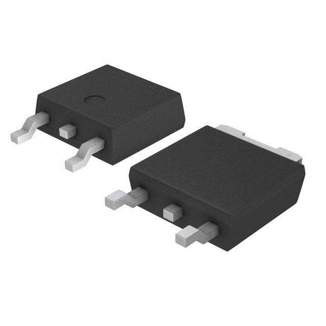
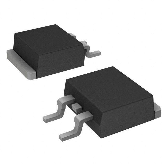
ICGOO电子元器件商城为您提供FDMS8680由Fairchild Semiconductor设计生产,在icgoo商城现货销售,并且可以通过原厂、代理商等渠道进行代购。 FDMS8680价格参考。Fairchild SemiconductorFDMS8680封装/规格:晶体管 - FET,MOSFET - 单, 表面贴装 N 沟道 30V 14A(Ta),35A(Tc) 2.5W(Ta),50W(Tc) 8-PQFN(5x6)。您可以下载FDMS8680参考资料、Datasheet数据手册功能说明书,资料中有FDMS8680 详细功能的应用电路图电压和使用方法及教程。
FDMS8680 是安森美半导体(ON Semiconductor)生产的一款高性能MOSFET器件,常用于电源管理和功率转换应用。其应用场景主要包括:

1. DC-DC转换器:适用于高效能同步整流降压(Buck)转换器,广泛应用于服务器、通信设备和工业电源中。

2. 负载开关与电源管理:因其低导通电阻(Rds(on))和高电流承载能力,适合用作负载开关,控制电源分配并减少功耗。

3. 电机驱动电路:在直流电机或步进电机的驱动模块中,作为功率开关元件使用,具备快速开关能力和良好热稳定性。

4. 电池管理系统(BMS):用于电池充放电控制电路中,提供高效的电流通断功能,并有助于提升系统安全性。

5. LED照明驱动:在高亮度LED驱动电路中作为开关元件,实现恒流控制和节能效果。

该器件采用先进的封装技术,具备优良的热性能和空间利用率,适合高密度电源设计,广泛应用于通信、工业自动化、消费电子及汽车电子等领域。
| 参数 | 数值 |
| 产品目录 | |
| ChannelMode | Enhancement |
| 描述 | MOSFET N-CH 30V 14A POWER56MOSFET 30V N-CHANNEL |
| 产品分类 | FET - 单分离式半导体 |
| FET功能 | 逻辑电平门 |
| FET类型 | MOSFET N 通道,金属氧化物 |
| Id-ContinuousDrainCurrent | 14 A |
| Id-连续漏极电流 | 14 A |
| 品牌 | Fairchild Semiconductor |
| 产品手册 | |
| 产品图片 |
|
| rohs | 符合RoHS无铅 / 符合限制有害物质指令(RoHS)规范要求 |
| 产品系列 | 晶体管,MOSFET,Fairchild Semiconductor FDMS8680PowerTrench® |
| 数据手册 | |
| 产品型号 | FDMS8680 |
| PCN其它 | |
| Pd-PowerDissipation | 2.5 W |
| Pd-功率耗散 | 2.5 W |
| RdsOn-Drain-SourceResistance | 8.5 mOhms |
| RdsOn-漏源导通电阻 | 8.5 mOhms |
| Vds-Drain-SourceBreakdownVoltage | 30 V |
| Vds-漏源极击穿电压 | 30 V |
| Vgs-Gate-SourceBreakdownVoltage | +/- 20 V |
| Vgs-栅源极击穿电压 | 20 V |
| 上升时间 | 3 ns |
| 下降时间 | 2 ns |
| 不同Id时的Vgs(th)(最大值) | 3V @ 250µA |
| 不同Vds时的输入电容(Ciss) | 1590pF @ 15V |
| 不同Vgs时的栅极电荷(Qg) | 26nC @ 10V |
| 不同 Id、Vgs时的 RdsOn(最大值) | 7 毫欧 @ 14A,10V |
| 产品种类 | MOSFET |
| 供应商器件封装 | Power56 |
| 其它名称 | FDMS8680DKR |
| 典型关闭延迟时间 | 21 ns |
| 功率-最大值 | 2.5W |
| 包装 | Digi-Reel® |
| 单位重量 | 90 mg |
| 商标 | Fairchild Semiconductor |
| 安装类型 | 表面贴装 |
| 安装风格 | SMD/SMT |
| 封装 | Reel |
| 封装/外壳 | 8-PQFN,Power56 |
| 封装/箱体 | Power 56-8 |
| 工厂包装数量 | 3000 |
| 晶体管极性 | N-Channel |
| 最大工作温度 | + 150 C |
| 最小工作温度 | - 55 C |
| 标准包装 | 1 |
| 正向跨导-最小值 | 72 S |
| 漏源极电压(Vdss) | 30V |
| 特色产品 | http://www.digikey.cn/product-highlights/cn/zh/fairchild-cloud-systems-computing/4301 |
| 电流-连续漏极(Id)(25°C时) | 14A (Ta), 35A (Tc) |
| 系列 | FDMS8680 |
| 通道模式 | Enhancement |
| 配置 | Single Quad Drain Triple Source |


.jpg)


PDF Datasheet 数据手册内容提取
Is Now Part of To learn more about ON Semiconductor, please visit our website at www.onsemi.com Please note: As part of the Fairchild Semiconductor integration, some of the Fairchild orderable part numbers will need to change in order to meet ON Semiconductor’s system requirements. Since the ON Semiconductor product management systems do not have the ability to manage part nomenclature that utilizes an underscore (_), the underscore (_) in the Fairchild part numbers will be changed to a dash (-). This document may contain device numbers with an underscore (_). Please check the ON Semiconductor website to verify the updated device numbers. The most current and up-to-date ordering information can be found at www.onsemi.com. Please email any questions regarding the system integration to Fairchild_questions@onsemi.com. ON Semiconductor and the ON Semiconductor logo are trademarks of Semiconductor Components Industries, LLC dba ON Semiconductor or its subsidiaries in the United States and/or other countries. ON Semiconductor owns the rights to a number of patents, trademarks, copyrights, trade secrets, and other intellectual property. A listing of ON Semiconductor’s product/patent coverage may be accessed at www.onsemi.com/site/pdf/Patent-Marking.pdf. ON Semiconductor reserves the right to make changes without further notice to any products herein. ON Semiconductor makes no warranty, representation or guarantee regarding the suitability of its products for any particular purpose, nor does ON Semiconductor assume any liability arising out of the application or use of any product or circuit, and specifically disclaims any and all liability, including without limitation special, consequential or incidental damages. Buyer is responsible for its products and applications using ON Semiconductor products, including compliance with all laws, regulations and safety requirements or standards, regardless of any support or applications information provided by ON Semiconductor. “Typical” parameters which may be provided in ON Semiconductor data sheets and/or specifications can and do vary in different applications and actual performance may vary over time. All operating parameters, including “Typicals” must be validated for each customer application by customer’s technical experts. ON Semiconductor does not convey any license under its patent rights nor the rights of others. ON Semiconductor products are not designed, intended, or authorized for use as a critical component in life support systems or any FDA Class 3 medical devices or medical devices with a same or similar classification in a foreign jurisdiction or any devices intended for implantation in the human body. Should Buyer purchase or use ON Semiconductor products for any such unintended or unauthorized application, Buyer shall indemnify and hold ON Semiconductor and its officers, employees, subsidiaries, affiliates, and distributors harmless against all claims, costs, damages, and expenses, and reasonable attorney fees arising out of, directly or indirectly, any claim of personal injury or death associated with such unintended or unauthorized use, even if such claim alleges that ON Semiconductor was negligent regarding the design or manufacture of the part. ON Semiconductor is an Equal Opportunity/Affirmative Action Employer. This literature is subject to all applicable copyright laws and is not for resale in any manner.
F D M S 8 6 October 2014 8 FDMS8680 0 N N-Channel PowerTrench® MOSFET(cid:3) tm -C h 30V, 35A, 7.0m(cid:58) a n Features General Description n e l (cid:132) Max rDS(on) = 7.0m(cid:58)(cid:3)at VGS = 10V, ID = 14A The FDMS8680 has been designed to minimize losses in power P conversion application. Advancements in both silicon and o (cid:132) Max rDS(on) = 11.0m(cid:58) at VGS = 4.5V, ID = 11.5A package technologies have been combined to offer the lowest w e (cid:132) Advanced Package and Silicon combination for rDS(on) while maintaining excellent switching performance. r low r and high efficiency T DS(on) Applications r e (cid:132) MSL1 robust package design (cid:132) Low Side for Synchronous Buck to Power Core Processor n c (cid:132) RoHS Compliant (cid:132) Secondary Side Synchronous Rectifier h® (cid:132) Low Side Switch in POL DC/DC Converter M O (cid:132) Oring FET/ Load Switch S F E T Top Bottom Pin 1 S D 5 4 G S S G D 6 3 S D 7 2 S D D D 8 1 S D D Power 56 MOSFET Maximum Ratings T = 25°C unless otherwise noted A Symbol Parameter Ratings Units V Drain to Source Voltage 30 V DS V Gate to Source Voltage ±20 V GS Drain Current -Continuous (Package limited) T = 25°C 35 C -Continuous (Silicon limited) T = 25°C 63 I C A D -Continuous T = 25°C (Note 1a) 14 A -Pulsed 100 E Single Pulse Avalanche Energy (Note 3) 216 mJ AS Power Dissipation T = 25°C 50 P C W D Power Dissipation T = 25°C (Note 1a) 2.5 A T , T Operating and Storage Junction Temperature Range -55 to +150 °C J STG Thermal Characteristics R Thermal Resistance, Junction to Case 2.5 (cid:84)JC °C/W R Thermal Resistance, Junction to Ambient (Note 1a) 50 (cid:84)JA Package Marking and Ordering Information Device Marking Device Package Reel Size Tape Width Quantity FDMS8680 FDMS8680 Power 56 13" 12mm 3000units ©2009 Fairchild Semiconductor Corporation 1 www.fairchildsemi.com FDMS8680 Rev.C3
F D Electrical Characteristics M T = 25°C unless otherwise noted J S Symbol Parameter Test Conditions Min Typ Max Units 8 6 8 Off Characteristics 0 N BVDSS Drain to Source Breakdown Voltage ID = 250(cid:80)A, VGS = 0V 30 V - (cid:39)(cid:3)(cid:3)(cid:3)B(cid:39)VTDJSS BCroeeaffkicdioewntn Voltage Temperature ID = 250(cid:80)A, referenced to 25°C 24 mV/°C Cha IDSS Zero Gate Voltage Drain Current VDS = 24V, VGS= 0V 1 (cid:80)A nn IGSS Gate to Source Leakage Current VGS = ±20V, VDS= 0V ±100 nA e l P On Characteristics o w VGS(th) Gate to Source Threshold Voltage VGS = VDS, ID = 250(cid:80)A 1.0 1.8 3.0 V e (cid:3)(cid:3)(cid:39)(cid:3)(cid:3)(cid:39)VTGJS(th) GTeamtep teor aStuoruer cCeo Tehffriceisehnotld Voltage ID = 250(cid:80)A, referenced to 25°C -5.7 mV/°C rTr e VGS = 10V, ID = 14A 5.5 7.0 n c rDS(on) Static Drain to Source On Resistance VGS = 4.5V, ID = 11.5A 8.5 11.0 m(cid:58) h V = 10V, I = 14A, T = 125°C 8.2 10.5 ® GS D J M g Forward Transconductance V = 10V, I = 14A 72 S FS DD D O Dynamic Characteristics S F C Input Capacitance 1195 1590 pF E iss V = 15V, V = 0V, T C Output Capacitance DS GS 555 740 pF oss f = 1MHz C Reverse Transfer Capacitance 95 145 pF rss Rg Gate Resistance f = 1MHz 0.8 4.0 (cid:58) Switching Characteristics t Turn-On Delay Time 9 18 ns d(on) V = 15V, I = 14A, t Rise Time DD D 3 10 ns tr Turn-Off Delay Time VGS = 10V, RGEN = 6(cid:58) 21 34 ns d(off) t Fall Time 2 10 ns f Q Total Gate Charge V = 0V to 10V 18 26 nC g GS V = 15V, Q Total Gate Charge V = 0V to 5V DD 10 14 nC g GS I = 14A Q Gate to Source Charge D 3.2 nC gs Q Gate to Drain “Miller” Charge 2.7 nC gd Drain-Source Diode Characteristics V Source to Drain Diode Forward Voltage V = 0V, I = 14A (Note 2) 0.8 1.2 V SD GS S t Reverse Recovery Time 27 44 ns Qrr Reverse Recovery Charge IF = 14A, di/dt = 100A/(cid:80)s 15 27 nC rr NOTES: 1. R(cid:84)JA is determined with the device mounted on a 1in2 pad 2 oz copper pad on a 1.5 x 1.5 in. board of FR-4 material. R(cid:84)JC isguaranteed by design while R(cid:84)CA is determined by the user's board design. a.50°C/W when mounted on a b. 125°C/W when mounted on a 1in2pad of 2 oz copper. minimum pad of 2 oz copper. 2. Pulse Test: Pulse Width < 300(cid:80)s, Duty cycle < 2.0%. 3. Starting TJ = 25°C, L = 3mH, IAS = 12A, VDD = 30V, VGS = 10V. ©2009 Fairchild Semiconductor Corporation 2 www.fairchildsemi.com FDMS8680 Rev.C3
F D Typical Characteristics M T = 25°C unless otherwise noted J S 8 6 100 4.0 8 V = 4V NCE 3.5 VGS =3V PDUULTSYE C DYUCRLEA T=I O0.N5 %= M80A(cid:80)Xs 0 N AIN CURRENT (A) 468000 VVGGSS == 41.05VV VGGSS = 3.5V NORMALIZEDOURCE ON-RESISTA 223...050 VGS =3.5V VGS = 4V -Channel P ,IDRD 20 VGS = 3V N TO S 11..05 VGS =4.5V owe PULSE DURATION = 80(cid:80)s AI r 0 DUTY CYCLE = 0.5%MAX DR 0.5 VGS =10V Tr 0 1 2 3 4 0 20 40 60 80 100 e n VDS,DRAIN TO SOURCE VOLTAGE (V) ID,DRAIN CURRENT(A) c h Figure 1. On-Region Characteristics Figure 2. Normalized On-Resistance ® vs Drain Current and Gate Voltage M O S 1.8 24 F STANCE 1.6 V IDG S= =1 41A0V )m(cid:58) 20 ID= 14A PDUULTSYE C DYUCRLEA T=I O0.N5 %= M80A(cid:80)Xs ET ESI 1.4 (E MALIZEDCE ON-R 1.2 RAIN TO SISTANC 16 NORN TO SOUR 01..80 r, DDS(on)RCE ON-RE 128 TJ= 125oC RAI OU TJ= 25oC D 0.6 S 4 -75 -50 -25 0 25 50 75 100 125 150 2 4 6 8 10 TJ,JUNCTION TEMPERATURE (oC) VGS,GATE TO SOURCE VOLTAGE (V) Figure 3. Normalized On- Resistance Figure 4. On-Resistance vs Gate to vs Junction Temperature Source Voltage 100 100 PULSE DURATION = 80(cid:80)s A) VGS = 0V DUTY CYCLE = 0.5%MAX T ( 80 N 10 A) VDD = 5V RE T ( UR RREN 60 AIN C 1 TJ = 25oC N CU 40 E DR 0.1 TJ= 150oC RAI TJ= 150oC ERS D V I, D 20 TJ = 25oC TJ = -55oC I, RES0.01 TJ = -55oC 0 0.001 1 2 3 4 5 0.0 0.2 0.4 0.6 0.8 1.0 1.2 VGS, GATE TO SOURCE VOLTAGE (V) VSD, BODY DIODE FORWARD VOLTAGE (V) Figure 5. Transfer Characteristics Figure 6. Source to Drain Diode Forward Voltage vs Source Current ©2009 Fairchild Semiconductor Corporation 3 www.fairchildsemi.com FDMS8680 Rev.C3
F D Typical Characteristics M T = 25°C unless otherwise noted J S 8 6 10 2000 8 V) ID= 14A Ciss 0 E( N G 8 1000 A - CE VOLT 6 VDD = 10V VDD = 15V CE (pF) Coss Chan UR VDD = 20V AN n O T e S 4 CI l E TO CAPA Po GAT 2 100 f = 1MHz Crss we V, GS 0 50 VGS = 0V rTr 0 4 8 12 16 20 0.1 1 10 30 e n Qg, GATE CHARGE(nC) VDS, DRAIN TO SOURCE VOLTAGE (V) c h Figure 7. Gate Charge Characteristics Figure 8. Capacitance vs Drain ® to Source Voltage M O S 20 70 F E NCHE CURRENT(A) 10 TJ= 25oC AIN CURRENT (A) 34560000 VGS= 10V T VALA TJ= 125oC ,DRD20 Limited by Package VGS= 4.5V A I , S 10 IA R(cid:84)JC = 2.5oC/W 1 0 0.01 0.1 1 10 100 300 25 50 75 100 125 150 tAV, TIME IN AVALANCHE(ms) TC,CASE TEMPERATURE (oC) Figure 9. Unclamped Inductive Figure 10. Maximum Continuous Drain Switching Capability Current vs Case Temperature 200 2000 100 100us R (W)1000 VGS = 10V SRING=L E1 2P5UoCL/SWE T (A) 10 OWE TA(cid:84)J=A 25oC AIN CURREN 1 TLIHMISIT AERDE BAY I SrD S(on) 11100m0msmss RANSIENT P 10100 DR SINGLE PULSE 1s K T I, D 0.1 TRJ= M= A1X25 RoCA/TWED 10s PEA 0.01 TA(cid:84)J=A 25oC DC ,P()PK 0.15 0.01 0.1 1 10 100 10-4 10-3 10-2 10-1 100 101 102 103 VDS, DRAIN to SOURCE VOLTAGE (V) t, PULSE WIDTH (s) Figure 11. Forward Bias Safe Figure 12. Single Pulse Maximum Operating Area Power Dissipation ©2009 Fairchild Semiconductor Corporation 4 www.fairchildsemi.com FDMS8680 Rev.C3
F D Typical Characteristics M T = 25°C unless otherwise noted J S 8 6 2 8 1 DUTY CYCLE-DESCENDING ORDER 0 N D = 0.5 - MAL A 0.1 00..21 Ch RMALIZED THERIMPEDANCE,ZJ(cid:84) 0.01 000...000521 PDM t1 annel Pow NO 0.001 SINGLE PULSE t2 e R = 125oC/W NOTES: r (cid:84)JA DUTY FACTOR: D = t1/t2 T PEAK TJ = PDM x Z(cid:84)JA x R(cid:84)JA + TA re 0.0001 n 10-4 10-3 10-2 10-1 100 101 102 103 c h t, RECTANGULAR PULSE DURATION (s) ® Figure 13. Transient Thermal Response Curve M O S F E T ©2009 Fairchild Semiconductor Corporation 5 www.fairchildsemi.com FDMS8680 Rev.C3
PQFN85X6,1.27P CASE483AE ISSUEA 5.10 A 5.10 3.91 PKG SEE CL B DETAILB 1.27 8 5 8 7 6 5 0.77 4.52 3.75 PKGCL 6.15 5.85 6.61 5.65 KEEPOUT AREA 1.27 1 4 1 2 3 4 TOPVIEW 1.27 0.61 3.81 LANDPATTERN OPTIONALDRAFT RECOMMENDATION ANGLEMAYAPPEAR SEE ONFOURSIDES 5.00 4.80 DETAILC OFTHEPACKAGE 0.35 0.15 (cid:19)(cid:131)(cid:16)(cid:20)(cid:21)(cid:131) 0.10 C 0.30 0.05 0.05 SIDEVIEW 0.00 (cid:19)(cid:131)(cid:16)(cid:20)(cid:21)(cid:131) 8X 0.08 C 0.35 C 5.20 0.15 4.80 1.10 SEATING 0.90 PLANE DETAILC DETAILB 3.81 SCALE:2:1 SCALE:2:1 1.27 0.51 (8X) 0.31 (0.34) NOTES:UNLESSOTHERWISESPECIFIED 0.10 C A B A.PACKAGESTANDARDREFERENCE:JEDECMO-240, 1 2 3 4 ISSUEA,VAR.AA,. B.DIMENSIONSDONOTINCLUDEBURRSORMOLDFLASH. 0.76 MOLDFLASHORBURRSDOESNOTEXCEED0.10MM. 0.51 (0.52) C.ALLDIMENSIONSAREINMILLIMETERS. 6.25 D.DIMENSIONINGANDTOLERANCINGPERASMEY14.5M-2009. 5.90 E.ITISRECOMMENDEDTOHAVENOTRACESOR VIASWITHINTHEKEEPOUTAREA. (0.50) 3.48+0.30 -0.10 (0.30) (2X) 8 7 6 5 +0.10 (cid:19)(cid:17)(cid:23)(cid:23)(cid:147)(cid:19)(cid:17)(cid:20)(cid:19) 0.20 (8X) 3.96 -0.15 3.61 BOTTOMVIEW
ON Semiconductor and are trademarks of Semiconductor Components Industries, LLC dba ON Semiconductor or its subsidiaries in the United States and/or other countries. ON Semiconductor owns the rights to a number of patents, trademarks, copyrights, trade secrets, and other intellectual property. A listing of ON Semiconductor’s product/patent coverage may be accessed at www.onsemi.com/site/pdf/Patent−Marking.pdf. ON Semiconductor reserves the right to make changes without further notice to any products herein. ON Semiconductor makes no warranty, representation or guarantee regarding the suitability of its products for any particular purpose, nor does ON Semiconductor assume any liability arising out of the application or use of any product or circuit, and specifically disclaims any and all liability, including without limitation special, consequential or incidental damages. Buyer is responsible for its products and applications using ON Semiconductor products, including compliance with all laws, regulations and safety requirements or standards, regardless of any support or applications information provided by ON Semiconductor. “Typical” parameters which may be provided in ON Semiconductor data sheets and/or specifications can and do vary in different applications and actual performance may vary over time. All operating parameters, including “Typicals” must be validated for each customer application by customer’s technical experts. ON Semiconductor does not convey any license under its patent rights nor the rights of others. ON Semiconductor products are not designed, intended, or authorized for use as a critical component in life support systems or any FDA Class 3 medical devices or medical devices with a same or similar classification in a foreign jurisdiction or any devices intended for implantation in the human body. Should Buyer purchase or use ON Semiconductor products for any such unintended or unauthorized application, Buyer shall indemnify and hold ON Semiconductor and its officers, employees, subsidiaries, affiliates, and distributors harmless against all claims, costs, damages, and expenses, and reasonable attorney fees arising out of, directly or indirectly, any claim of personal injury or death associated with such unintended or unauthorized use, even if such claim alleges that ON Semiconductor was negligent regarding the design or manufacture of the part. ON Semiconductor is an Equal Opportunity/Affirmative Action Employer. This literature is subject to all applicable copyright laws and is not for resale in any manner. PUBLICATION ORDERING INFORMATION LITERATURE FULFILLMENT: N. American Technical Support: 800−282−9855 Toll Free ON Semiconductor Website: www.onsemi.com Literature Distribution Center for ON Semiconductor USA/Canada 19521 E. 32nd Pkwy, Aurora, Colorado 80011 USA Europe, Middle East and Africa Technical Support: Order Literature: http://www.onsemi.com/orderlit Phone: 303−675−2175 or 800−344−3860 Toll Free USA/Canada Phone: 421 33 790 2910 Fax: 303−675−2176 or 800−344−3867 Toll Free USA/Canada Japan Customer Focus Center For additional information, please contact your local Email: orderlit@onsemi.com Phone: 81−3−5817−1050 Sales Representative © Semiconductor Components Industries, LLC www.onsemi.com www.onsemi.com 1
Mouser Electronics Authorized Distributor Click to View Pricing, Inventory, Delivery & Lifecycle Information: O N Semiconductor: FDMS8680