ICGOO在线商城 > 分立半导体产品 > 晶体管 - FET,MOSFET - 阵列 > CSD87353Q5D

 Datasheet下载
- 型号: CSD87353Q5D
- 制造商: Texas Instruments
- 库位|库存: xxxx|xxxx
- 要求:
| 数量阶梯 | 香港交货 | 国内含税 |
| +xxxx | $xxxx | ¥xxxx |
查看当月历史价格
查看今年历史价格
CSD87353Q5D产品简介:
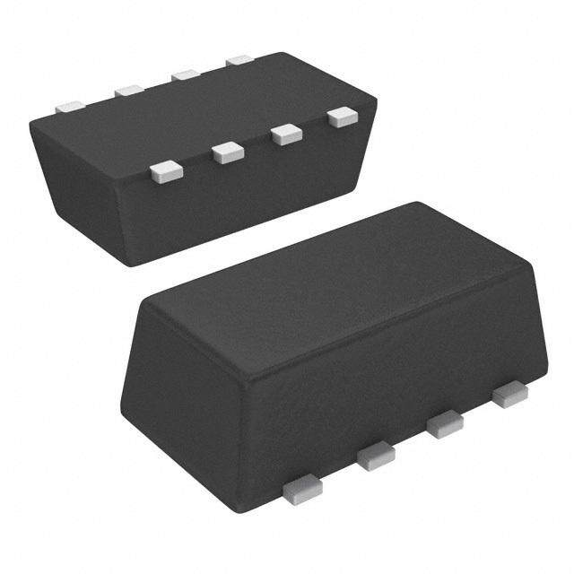
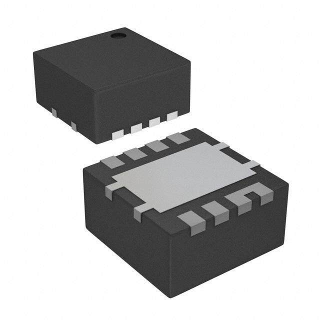
ICGOO电子元器件商城为您提供CSD87353Q5D由Texas Instruments设计生产,在icgoo商城现货销售,并且可以通过原厂、代理商等渠道进行代购。 CSD87353Q5D价格参考。Texas InstrumentsCSD87353Q5D封装/规格:晶体管 - FET,MOSFET - 阵列, 2 个 N 通道(半桥) Mosfet 阵列 30V 40A 12W 表面贴装 8-LSON(5x6)。您可以下载CSD87353Q5D参考资料、Datasheet数据手册功能说明书,资料中有CSD87353Q5D 详细功能的应用电路图电压和使用方法及教程。
CSD87353Q5D 是由 Texas Instruments(德州仪器)生产的一款晶体管 - FET,MOSFET - 阵列产品。该型号属于 NexFET 功率 MOSFET 系列,广泛应用于高效能电源管理领域。以下是其主要应用场景:

1. DC-DC 转换器:
   CSD87353Q5D 适用于开关模式电源(SMPS)中的 DC-DC 转换器设计,特别是降压(Buck)和升压(Boost)转换器。其低导通电阻(Rds(on))特性能够显著降低功率损耗,提高整体效率。

2. 电机驱动:
   在小型电机控制应用中,如无人机、机器人、家用电器等,CSD87353Q5D 可作为功率级驱动元件,提供高效的电流切换能力。

3. 电池管理系统(BMS):
   用于锂电池保护电路或电池充放电管理,确保电流在安全范围内流动,并实现快速开关以保护电池免受过流或短路的影响。

4. 负载开关:
   在便携式电子设备(如智能手机、平板电脑)中,该器件可用作负载开关,实现快速开启/关闭功能,同时减少静态功耗。

5. 多相供电系统:
   在高性能计算、图形卡(GPU)及 FPGA 的供电模块中,CSD87353Q5D 能够支持多相供电架构,为处理器提供稳定且高效的电流供应。

6. LED 驱动:
   在高亮度 LED 照明应用中,该器件可作为开关元件,用于调节 LED 的亮度和颜色,同时保持较低的热损耗。

总结来说,CSD87353Q5D 凭借其卓越的电气性能和紧凑封装,非常适合需要高效、低损耗和快速开关的应用场景,特别是在消费电子、工业自动化和通信设备等领域中发挥重要作用。
| 参数 | 数值 |
| 产品目录 | |
| 描述 | MOSFET 2N-CH 30V 40A 8LSONMOSFET 30V Sync Buck NexFET Power Block |
| 产品分类 | FET - 阵列分离式半导体 |
| FET功能 | 逻辑电平门 |
| FET类型 | 2 个 N 通道(半桥) |
| Id-ContinuousDrainCurrent | 40 A |
| Id-连续漏极电流 | 40 A |
| 品牌 | Texas Instruments |
| 产品手册 | |
| 产品图片 |
|
| rohs | 符合RoHS含铅 / 不受限制有害物质指令(RoHS)规范要求限制 |
| 产品系列 | 晶体管,MOSFET,Texas Instruments CSD87353Q5DNexFET™ |
| 数据手册 | |
| 产品型号 | CSD87353Q5D |
| PCN封装 | |
| PCN组件/产地 | |
| PCN设计/规格 | |
| Pd-PowerDissipation | 12 W |
| Pd-功率耗散 | 12 W |
| Qg-GateCharge | 16 nC, 20 nC |
| Qg-栅极电荷 | 16 nC, 20 nC |
| RdsOn-Drain-SourceResistance | 8.5 mOhms |
| RdsOn-漏源导通电阻 | 8.5 mOhms |
| Vds-Drain-SourceBreakdownVoltage | 30 V |
| Vds-漏源极击穿电压 | 30 V |
| Vgs-Gate-SourceBreakdownVoltage | 2.1 V, 1.15 V |
| Vgs-栅源极击穿电压 | 10 V |
| 上升时间 | 16 ns, 10 ns |
| 下降时间 | 4 ns, 4.6 ns |
| 不同Id时的Vgs(th)(最大值) | 2.1V @ 250µA |
| 不同Vds时的输入电容(Ciss) | 3190pF @ 15V |
| 不同Vgs时的栅极电荷(Qg) | 19nC @ 4.5V |
| 不同 Id、Vgs时的 RdsOn(最大值) | 3.4 欧姆 @ 4.5V |
| 产品培训模块 | http://www.digikey.cn/PTM/IndividualPTM.page?site=cn&lang=zhs&ptm=25585http://www.digikey.cn/PTM/IndividualPTM.page?site=cn&lang=zhs&ptm=25886 |
| 产品种类 | MOSFET |
| 供应商器件封装 | 8-LSON (5x6) |
| 其它名称 | 296-29661-6 |
| 典型关闭延迟时间 | 20 ns, 23 ns |
| 制造商产品页 | http://www.ti.com/general/docs/suppproductinfo.tsp?distId=10&orderablePartNumber=CSD87353Q5D |
| 功率-最大值 | 12W |
| 包装 | Digi-Reel® |
| 商标 | Texas Instruments |
| 商标名 | NexFET |
| 安装类型 | 表面贴装 |
| 安装风格 | SMD/SMT |
| 封装 | Reel |
| 封装/外壳 | 8-LDFN 裸露焊盘 |
| 封装/箱体 | LSON-8 Clip |
| 工厂包装数量 | 2500 |
| 晶体管极性 | N-Channel |
| 最大工作温度 | + 150 C |
| 最小工作温度 | - 55 C |
| 标准包装 | 1 |
| 正向跨导-最小值 | 160 S / 135 S |
| 漏源极电压(Vdss) | 30V |
| 电流-连续漏极(Id)(25°C时) | 40A |
| 系列 | CSD87353Q5D |
| 配置 | Dual |


- 商务部:美国ITC正式对集成电路等产品启动337调查
- 曝三星4nm工艺存在良率问题 高通将骁龙8 Gen1或转产台积电
- 太阳诱电将投资9.5亿元在常州建新厂生产MLCC 预计2023年完工
- 英特尔发布欧洲新工厂建设计划 深化IDM 2.0 战略
- 台积电先进制程称霸业界 有大客户加持明年业绩稳了
- 达到5530亿美元!SIA预计今年全球半导体销售额将创下新高
- 英特尔拟将自动驾驶子公司Mobileye上市 估值或超500亿美元
- 三星加码芯片和SET,合并消费电子和移动部门,撤换高东真等 CEO
- 三星电子宣布重大人事变动 还合并消费电子和移动部门
- 海关总署:前11个月进口集成电路产品价值2.52万亿元 增长14.8%
PDF Datasheet 数据手册内容提取
Product Order Technical Tools & Support & Folder Now Documents Software Community CSD87353Q5D SLPS285D–AUGUST2011–REVISEDFEBRUARY2017 CSD87353Q5D Synchronous Buck NexFET™ Power Block 1 Features 3 Description • V upto27V The CSD87353Q5D NexFET™ power block is an 1 IN optimized design for synchronous buck applications • Half-BridgePowerBlock offering high-current, high-efficiency, and high- • 95%SystemEfficiencyat25A frequency capability in a small 5-mm × 6-mm outline. • Upto40-AOperation Optimized for 5-V gate drive applications, this product offers a flexible solution capable of offering a high- • High-FrequencyOperation(upto1.5MHz) density power supply when paired with any 5-V gate • High-DensitySON5-mm×6-mmFootprint drivefromanexternalcontroller/driver. • Optimizedfor5-VGateDrive TopView • Low-SwitchingLosses • Ultra-Low-InductancePackage VIN 1 8 VSW • RoHSCompliant VIN 2 7 VSW • HalogenFree PGND (Pin 9) • Lead-FreeTerminalPlating TG 3 6 VSW TGR 4 5 BG 2 Applications P0116-01 • SynchronousBuckConverters DeviceInformation(1) – High-FrequencyApplications DEVICE MEDIA QTY PACKAGE SHIP – High-Current,High-DutyCycleApplications SON Tapeand CSD87353Q5D 13-InchReel 2500 5-mm×6-mm • MultiphaseSynchronousBuckConverters Reel PlasticPackage • POLDC-DCConverters (1) For all available packages, see the orderable addendum at • IMVP,VRM,andVRDApplications theendofthedatasheet. TypicalCircuit TypicalPowerBlockEfficiencyandPowerLoss 100 12 95 10 Efficiency (%) 889050 VVVLfSOGIOWNUSU T= =T= ==1 55 2003VV0..63k8VHµzH 468 Power Loss (W) TA = 25ºC 75 2 70 0 0 5 10 15 20 25 30 35 40 Output Current (A) 1 An IMPORTANT NOTICE at the end of this data sheet addresses availability, warranty, changes, use in safety-critical applications, intellectualpropertymattersandotherimportantdisclaimers.PRODUCTIONDATA.
CSD87353Q5D SLPS285D–AUGUST2011–REVISEDFEBRUARY2017 www.ti.com Table of Contents 1 Features.................................................................. 1 7 Layout................................................................... 15 2 Applications........................................................... 1 7.1 LayoutGuidelines...................................................15 3 Description............................................................. 1 7.2 LayoutExample......................................................16 4 RevisionHistory..................................................... 2 8 DeviceandDocumentationSupport.................. 17 5 Specifications......................................................... 3 8.1 DocumentationSupport..........................................17 5.1 AbsoluteMaximumRatings......................................3 8.2 ReceivingNotificationofDocumentationUpdates..17 5.2 RecommendedOperatingConditions.......................3 8.3 CommunityResources............................................17 5.3 PowerBlockPerformance........................................3 8.4 Trademarks.............................................................17 5.4 ThermalInformation..................................................3 8.5 ElectrostaticDischargeCaution..............................17 5.5 ElectricalCharacteristics...........................................4 8.6 Glossary..................................................................17 5.6 TypicalPowerBlockDeviceCharacteristics.............5 9 Mechanical,Packaging,andOrderable Information........................................................... 18 5.7 TypicalPowerBlockMOSFETCharacteristics.........7 9.1 Q5DPackageDimensions......................................18 6 ApplicationandImplementation........................ 10 9.2 LandPatternRecommendation..............................19 6.1 ApplicationInformation............................................10 9.3 StencilRecommendation........................................19 6.2 TypicalApplication..................................................13 9.4 Q5DTapeandReelInformation.............................20 4 Revision History NOTE:Pagenumbersforpreviousrevisionsmaydifferfrompagenumbersinthecurrentversion. ChangesfromRevisionC(October2011)toRevisionD Page • AddednoteforI intheAbsoluteMaximumRatingstable.................................................................................................. 3 DM • ChangedRecommendedPCBDesignOverviewsectiontoLayoutsection........................................................................ 15 • AddedDeviceandDocumentationSupportsection............................................................................................................. 17 • ChangedMechanicalDatasectiontoMechanical,Packaging,andOrderableInformationsection.................................... 18 ChangesfromRevisionB(September2011)toRevisionC Page • ChangedtheROCtable,OperatingCurrentMaxvalueFrom:25ATo:40A. ..................................................................... 3 ChangesfromRevisionA(September2011)toRevisionB Page • ChangeSyncFETUISFrom:500mJTo:551mJ. .............................................................................................................. 3 • ChangeControlFETUISFrom:245mJTo:378mJ. ........................................................................................................... 3 • ChangeControlFETRgvalues. ........................................................................................................................................... 4 • ChangeSyncFETRgvalues. ............................................................................................................................................... 4 • UpdatedFigure26. ................................................................................................................................................................ 9 ChangesfromOriginal(August2011)toRevisionA Page • ChangedApplicationbulletFrom:HighCurrent,LowDutyCycleApplicationsTo:HighCurrent,HighDutyCycle Applications. .......................................................................................................................................................................... 1 • RemoveZ Max............................................................................................................................................................... 4 DS(on) • DeletedtheZ MaxvaluesintheComparisontable. .................................................................................................... 12 DS(on) • AddElectricalPerformancebullet. ...................................................................................................................................... 15 2 SubmitDocumentationFeedback Copyright©2011–2017,TexasInstrumentsIncorporated ProductFolderLinks:CSD87353Q5D
CSD87353Q5D www.ti.com SLPS285D–AUGUST2011–REVISEDFEBRUARY2017 5 Specifications 5.1 Absolute Maximum Ratings T =25°C(unlessotherwisenoted)(1) A PARAMETER CONDITIONS MIN MAX UNIT V toP 30 V IN GND V toP 30 V SW GND Voltage V toP (10ns) 32 V SW GND T toT –8 10 V G GR B toP –8 10 V G GND Pulsedcurrentrating,I (2) 120 A DM Powerdissipation,P 12 W D SyncFET,I =105A,L=0.1mH 551 D Avalancheenergy,E mJ AS ControlFET,I =87A,L=0.1mH 378 D Operatingjunction,T –55 150 °C J Storagetemperature,T –55 150 °C STG (1) StressesbeyondthoselistedunderAbsoluteMaximumRatingsmaycausepermanentdamagetothedevice.Thesearestressratings only,andfunctionaloperationofthedeviceattheseoranyotherconditionsbeyondthoseindicatedintheRecommendedOperating Conditionsisnotimplied.Exposuretoabsolute-maximum-ratedconditionsforextendedperiodsmayaffectdevicereliability. (2) Pulseduration≤50µs.Dutycycle≤0.01%. 5.2 Recommended Operating Conditions T =25°C(unlessotherwisenoted) A PARAMETER CONDITIONS MIN MAX UNIT Gatedrivevoltage,V 4.5 8 V GS Inputsupplyvoltage,V 27 V IN Switchingfrequency,ƒ C =0.1μF(min) 1500 kHz SW BST Operatingcurrent 40 A Operatingtemperature,T 125 °C J 5.3 Power Block Performance T =25°C(unlessotherwisenoted) A PARAMETER CONDITIONS MIN TYP MAX UNIT V =12V,V =5V,V =3.3V, IN GS OUT Powerloss,P (1) I =25A,ƒ =500kHz, 3.3 W LOSS OUT SW L =0.68µH,T =25°C OUT J V quiescentcurrent,I T toT =0V,B toP =0V 10 µA IN QVIN G GR G GND (1) Measurementmadewithsix10-µF(TDKC3216X5R1C106KTorequivalent)ceramiccapacitorsplacedacrossV toP pinsand IN GND usingahighcurrent5-VdriverIC. 5.4 Thermal Information T =25°C(unlessotherwisestated) A THERMALMETRIC MIN TYP MAX UNIT Junction-to-ambientthermalresistance(minCu)(1)(2) 102 R °C/W θJA Junction-to-ambientthermalresistance(maxCu)(1)(2) 50 Junction-to-casethermalresistance(topofpackage)(2) 20 R °C/W θJC Junction-to-casethermalresistance(P pin)(2) 2 GND (1) DevicemountedonFR4materialwith1-in2(6.45-cm2)Cu. (2) R isdeterminedwiththedevicemountedona1-in2(6.45-cm2),2oz(0.071-mm)thickCupadona1.5-in×1.5-in θJC (3.81-cm×3.81-cm),0.06-in(1.52-mm)thickFR4board.R isspecifiedbydesignwhileR isdeterminedbytheuser’sboard θJC θJA design. Copyright©2011–2017,TexasInstrumentsIncorporated SubmitDocumentationFeedback 3 ProductFolderLinks:CSD87353Q5D
CSD87353Q5D SLPS285D–AUGUST2011–REVISEDFEBRUARY2017 www.ti.com 5.5 Electrical Characteristics T =25°C(unlessotherwisestated) A Q1ControlFET Q2SyncFET PARAMETER TESTCONDITIONS UNIT MIN TYP MAX MIN TYP MAX STATICCHARACTERISTICS BV Drain-to-sourcevoltage V =0V,I =250μA 30 30 V DSS GS DS Drain-to-sourceleakage I V =0V,V =20V 1 1 μA DSS current GS DS Gate-to-sourceleakage I V =0V,V =+10/–8V 100 100 nA GSS current DS GS Gate-to-sourcethreshold V V =V ,I =250μA 1.1 2.1 0.75 1.15 V GS(th) voltage DS GS DS V =12V,V =5V, IN GS Z (1) EffectiveACon-impedance VOUT=3.3V,IOUT=20A, 2.8 0.9 mΩ DS(on) ƒ =500kHz, SW L =0.68µH OUT g Transconductance V =15V,I =20A 135 160 S fs DS DS DYNAMICCHARACTERISTICS C Inputcapacitance 2660 3190 2910 3490 pF ISS C Outputcapacitance V =0V,V =15V, 1100 1320 1320 1580 pF OSS GS DS ƒ=1MHz Reversetransfer C 43 54 51 68 pF RSS capacitance R Seriesgateresistance 0.9 2 0.7 1.5 Ω G Q Gatechargetotal(4.5V) 16 19 20 24 nC g Qgd Gatechargegate-to-drain VDS=15V, 3 3.6 nC Qgs Gatechargegate-to-source IDS=20A 4.9 4.2 nC Q GatechargeatVth 2.8 2.4 nC g(th) Q Outputcharge V =17V,V =0V 22 26 nC OSS DS GS t Turnondelaytime 10 8.5 ns d(on) tr Risetime VDS=15V,VGS=4.5V, 16 10 ns td(off) Turnoffdelaytime IDS=20A,RG=2Ω 20 23 ns t Falltime 4 4.6 ns f DIODECHARACTERISTICS V Diodeforwardvoltage I =20A,V =0V 0.8 1 0.8 1 V SD DS GS Qrr Reverserecoverycharge Vdd=17V,IF=20A, 29 33 nC t Reverserecoverytime di/dt=300A/μs 25 27 ns rr (1) Equivalentsystemperformancebasedonapplicationtesting.SeeApplicationandImplementationsectionfordetails. HD LD HD LD 5 5 x6 QFN MwhaexnRmθJoAu=nt5e0d°Con/W1in2 x6 QFN MwhaexnRmθJoAu=nt1e0d2o°Cn/W T T minimumpadareaof TA (6.45cm2)of2-oz TA M M 2-oz(0.071-mm)thick IN (0.071-mm)thickCu. IN Cu. R R e e v v 1 1 LG HS LG HS HG LS HG LS M0189-01 M0190-01 4 SubmitDocumentationFeedback Copyright©2011–2017,TexasInstrumentsIncorporated ProductFolderLinks:CSD87353Q5D
CSD87353Q5D www.ti.com SLPS285D–AUGUST2011–REVISEDFEBRUARY2017 5.6 Typical Power Block Device Characteristics Testconditions:V =12V,V =5V,ƒ =500kHz,V =3.3V,L =0.68µH,I =40A,T =125°C,unlessstated IN GS SW OUT OUT OUT J otherwise. 10 1.4 9 1.3 8 1.2 d e 7 z 1.1 W) mali s ( 6 or 1 wer Los 45 Loss, N 00..89 Po er 3 w 0.7 o P 2 0.6 1 0.5 0 0.4 0 5 10 15 20 25 30 35 40 −50 −25 0 25 50 75 100 125 150 Output Current (A) Junction Temperature (ºC) Figure1.PowerLossvsOutputCurrent Figure2.NormalizedPowerLossvsTemperature 50 50 45 45 40 40 A) 35 A) 35 nt ( 30 nt ( 30 e e urr 25 urr 25 C C ut 20 ut 20 p p ut ut O 15 O 15 400LFM 400LFM 10 200LFM 10 200LFM 100LFM 100LFM 5 5 Nat Conv Nat Conv 0 0 0 10 20 30 40 50 60 70 80 90 0 10 20 30 40 50 60 70 80 90 Ambient Temperature (ºC) Ambient Temperature (ºC) Figure3.SafeOperatingArea–PCBVerticalMount(1) Figure4.SafeOperatingArea–PCBHorizontalMount(1) 50 45 40 A) 35 nt ( 30 e urr 25 C ut 20 p ut O 15 10 5 0 0 20 40 60 80 100 120 140 Board Temperature (ºC) Figure5.TypicalSafeOperatingArea(1) (1) The typical power block system characteristic curves are based on measurements made on a PCB design with dimensionsof4in(W)×3.5in(L)×0.062in(H)and6copperlayersof1-ozcopperthickness.SeeApplicationand Implementationsectionfordetailedexplanation. Copyright©2011–2017,TexasInstrumentsIncorporated SubmitDocumentationFeedback 5 ProductFolderLinks:CSD87353Q5D
CSD87353Q5D SLPS285D–AUGUST2011–REVISEDFEBRUARY2017 www.ti.com Typical Power Block Device Characteristics (continued) Testconditions:V =12V,V =5V,ƒ =500kHz,V =3.3V,L =0.68µH,I =40A,T =125°C,unlessstated IN GS SW OUT OUT OUT J otherwise. 1.6 5.1 1.6 5.3 1.5 4.3 1.5 4.4 d 1.4 3.4 C) d 1.4 3.5 C) Loss, Normalize 111...1123 0012....0976 mperature Adj (º Loss, Normalize 111...1123 0012....0986 mperature Adj (º er Te er Te Pow 0.9 −0.9 OA Pow 0.9 −0.9 OA 0.8 −1.7 S 0.8 −1.8 S 0.7 −2.6 0.7 −2.6 0.6 −3.4 0.6 −3.5 100 300 500 700 900 1100 1300 1500 1700 3 5 7 9 11 13 15 17 19 21 23 Switching Frequency (kHz) Input Voltage (V) Figure6.NormalizedPowerLossvsSwitchingFrequency Figure7.NormalizedPowerLossvsInputVoltage 1.6 4.9 1.6 5.3 1.5 4.1 1.5 4.4 d 1.4 3.2 C) d 1.4 3.5 C) Loss, Normalize 111...1123 0012...864 mperature Adj (º Loss, Normalize 111...1123 0012...987 mperature Adj (º er Te er Te Pow 0.9 −0.8 OA Pow 0.9 −0.9 OA 0.8 −1.6 S 0.8 −1.8 S 0.7 −2.4 0.7 −2.7 0.6 −3.2 0.6 −3.5 0 0.5 1 1.5 2 2.5 3 3.5 4 4.5 5 5.5 6 0.2 0.4 0.6 0.8 1 1.2 1.4 1.6 1.8 2 Output Voltage (V) Output Inductance (µH) Figure8.NormalizedPowerLossvsOutputVoltage Figure9.NormalizedPowerLossvsOutputInductance 6 SubmitDocumentationFeedback Copyright©2011–2017,TexasInstrumentsIncorporated ProductFolderLinks:CSD87353Q5D
CSD87353Q5D www.ti.com SLPS285D–AUGUST2011–REVISEDFEBRUARY2017 5.7 Typical Power Block MOSFET Characteristics T =25°C,unlessstatedotherwise. A 80 80 70 70 A A nt - 60 nt - 60 e e urr urr C 50 C 50 e e c c our 40 our 40 S S o- o- n-t 30 n-t 30 ai ai Dr 20 Dr 20 - S VGS = 8.0V - S VGS = 8.0V ID 10 VGS = 4.5V ID 10 VGS = 4.5V VGS = 4.0V VGS = 4.0V 0 0 0 0.05 0.1 0.15 0.2 0.25 0.3 0.35 0.4 0 0.05 0.1 0.15 0.2 0.25 VDS - Drain-to-Source Voltage - V VDS - Drain-to-Source Voltage - V Figure10.ControlMOSFETSaturation Figure11.SyncMOSFETSaturation 100 100 VDS = 5V VDS = 5V A A nt - 10 nt - 10 e e urr urr C C e 1 e 1 c c ur ur o o S S o- 0.1 o- 0.1 n-t n-t ai ai Dr Dr - S0.01 TC = 125°C - S0.01 TC = 125°C ID TC = 25°C ID TC = 25°C TC = −55°C TC = −55°C 0.001 0.001 0.5 1 1.5 2 2.5 3 0 0.5 1 1.5 2 2.5 VGS - Gate-to-Source Voltage - V VGS - Gate-to-Source Voltage - V Figure12.ControlMOSFETTransfer Figure13.SyncMOSFETTransfer 8 8 ID = 20A ID = 20A V) 7 VDD = 15V V) 7 VDD = 15V e ( e ( g 6 g 6 a a olt olt e V 5 e V 5 c c our 4 our 4 S S o- o- e-t 3 e-t 3 at at G G - S 2 - S 2 G G V 1 V 1 0 0 0 5 10 15 20 25 30 0 5 10 15 20 25 30 35 Qg - Gate Charge - nC (nC) Qg - Gate Charge - nC (nC) Figure14.ControlMOSFETGateCharge Figure15.SyncMOSFETGateCharge Copyright©2011–2017,TexasInstrumentsIncorporated SubmitDocumentationFeedback 7 ProductFolderLinks:CSD87353Q5D
CSD87353Q5D SLPS285D–AUGUST2011–REVISEDFEBRUARY2017 www.ti.com Typical Power Block MOSFET Characteristics (continued) T =25°C,unlessstatedotherwise. A 10 10 F 1 F 1 n n − − e e c c n n a a cit 0.1 cit 0.1 a a p p a a C C − − C 0.01 C 0.01 Ciss = Cgd + Cgs Ciss = Cgd + Cgs Coss = Cds + Cgd f = 1MHz Coss = Cds + Cgd f = 1MHz Crss = Cgd VGS = 0V Crss = Cgd VGS = 0V 0.001 0.001 0 5 10 15 20 25 30 0 5 10 15 20 25 30 VDS - Drain-to-Source Voltage - V VDS - Drain-to-Source Voltage - V Figure16.ControlMOSFETCapacitance Figure17.SyncMOSFETCapacitance 1.6 1.6 ID = 250µA ID = 250µA 1.4 1.4 V V e - 1.2 e - 1.2 g g a a Volt 1 Volt 1 d d hol 0.8 hol 0.8 s s e e Thr 0.6 Thr 0.6 - ()Sth 0.4 - ()Sth 0.4 G G V V 0.2 0.2 0 0 −75 −25 25 75 125 175 −75 −25 25 75 125 175 TC - Case Temperature - ºC TC - Case Temperature - ºC Figure18.ControlMOSFETV Figure19.SyncMOSFETV GS(th) GS(th) 8 8 ID = 20A ID = 20A 7 7 Wm Wm e - 6 e - 6 c c n n a a st 5 st 5 si si e e R R e 4 e 4 at at n-St 3 n-St 3 O O - ()Son 2 - ()Son 2 RD 1 TC = 25°C RD 1 TC = 25°C TC = 125ºC TC = 125ºC 0 0 0 1 2 3 4 5 6 7 8 9 10 0 1 2 3 4 5 6 7 8 9 10 VGS - Gate-to- Source Voltage - V VGS - Gate-to- Source Voltage - V Figure20.ControlMOSFETR vsV Figure21.SyncMOSFETR vsV DS(on) GS DS(on) GS 8 SubmitDocumentationFeedback Copyright©2011–2017,TexasInstrumentsIncorporated ProductFolderLinks:CSD87353Q5D
CSD87353Q5D www.ti.com SLPS285D–AUGUST2011–REVISEDFEBRUARY2017 Typical Power Block MOSFET Characteristics (continued) T =25°C,unlessstatedotherwise. A 1.8 1.8 ID = 20A ID = 20A e 1.6 VGS = 4.5V e 1.6 VGS = 4.5V c c an 1.4 an 1.4 st st si si e 1.2 e 1.2 R R e e at 1 at 1 St St n- 0.8 n- 0.8 O O d d e 0.6 e 0.6 z z ali ali m 0.4 m 0.4 or or N N 0.2 0.2 0 0 −75 −25 25 75 125 175 −75 −25 25 75 125 175 TC - Case Temperature - ºC TC - Case Temperature - ºC Figure22.ControlMOSFETNormalizedR Figure23.SyncMOSFETNormalizedR DS(on) DS(on) 100 100 A A nt - 10 nt - 10 e e urr 1 urr 1 C C n n ai ai Dr 0.1 Dr 0.1 o- o- e-t e-t c c ur 0.01 ur 0.01 o o S S − − D 0.001 D 0.001 IS TC = 25°C IS TC = 25°C TC = 125°C TC = 125°C 0.0001 0.0001 0 0.2 0.4 0.6 0.8 1 0 0.2 0.4 0.6 0.8 1 VSD − Source-to-Drain Voltage - V VSD − Source-to-Drain Voltage - V Figure24.ControlMOSFETBodyDiode Figure25.SyncMOSFETBodyDiode 1000 1000 A A nt - nt - e e Curr 100 Curr 100 e e h h c c n n a a al al v v A A ak 10 ak 10 e e P P - )V - )V I(A TC = 25°C I(A TC = 25°C TC = 125°C TC = 125°C 1 1 0.01 0.1 1 10 0.01 0.1 1 10 t(AV) - Time in Avalanche - ms t(AV) - Time in Avalanche - ms Figure26.ControlMOSFETUnclampedInductiveSwitching Figure27.SyncMOSFETUnclampedInductiveSwitching Copyright©2011–2017,TexasInstrumentsIncorporated SubmitDocumentationFeedback 9 ProductFolderLinks:CSD87353Q5D
CSD87353Q5D SLPS285D–AUGUST2011–REVISEDFEBRUARY2017 www.ti.com 6 Application and Implementation NOTE Information in the following applications sections is not part of the TI component specification, and TI does not warrant its accuracy or completeness. TI’s customers are responsible for determining suitability of components for their purposes. Customers should validateandtesttheirdesignimplementationtoconfirmsystemfunctionality. 6.1 Application Information 6.1.1 EquivalentSystemPerformance Many of today’s high-performance computing systems require low power consumption in an effort to reduce system operating temperatures and improve overall system efficiency. This has created a major emphasis on improving the conversion efficiency of today’s synchronous buck topology. In particular, there has been an emphasis in improving the performance of the critical power semiconductor in the power stage of this application (see Figure 28). As such, optimization of the power semiconductors in these applications, needs to go beyond simplyreducingR . DS(ON) Figure28. EquivalentSystemSchematic The CSD87353Q5D is part of TI’s power block product family which is a highly optimized product for use in a synchronous buck topology requiring high current, high efficiency, and high frequency. It incorporates TI’s latest generation silicon which has been optimized for switching performance, as well as minimizing losses associated with Q , Q , and Q . Furthermore, TI’s patented packaging technology has minimized losses by nearly GD GS RR eliminating parasitic elements between the control FET and sync FET connections (see Figure 29). A key challenge solved by TI’s patented packaging technology is the system level impact of Common Source Inductance (CSI). CSI greatly impedes the switching characteristics of any MOSFET which in turn increases switching losses and reduces system efficiency. As a result, the effects of CSI need to be considered during the MOSFET selection process. In addition, standard MOSFET switching loss equations used to predict system efficiency need to be modified in order to account for the effects of CSI. Further details behind the effects of CSI and modification of switching loss equations are outlined in Power Loss Calculation With Common Source InductanceConsiderationforSynchronousBuckConverters(SLPA009). 10 SubmitDocumentationFeedback Copyright©2011–2017,TexasInstrumentsIncorporated ProductFolderLinks:CSD87353Q5D
CSD87353Q5D www.ti.com SLPS285D–AUGUST2011–REVISEDFEBRUARY2017 Application Information (continued) Figure29. EliminationofParasiticInductances The combination of TI’s latest generation silicon and optimized packaging technology has created a benchmarking solution that outperforms industry standard MOSFET chipsets of similar R and MOSFET DS(ON) chipsets with lower R . Figure 30 and Figure 31 compare the efficiency and power loss performance of the DS(ON) CSD87353Q5D versus industry standard MOSFET chipsets commonly used in this type of application. This comparison purely focuses on the efficiency and generated loss of the power semiconductors only. The performance of CSD87353Q5D clearly highlights the importance of considering the effective AC on-impedance (Z ) during the MOSFET selection process of any new design. Simply normalizing to traditional MOSFET DS(ON) R specifications is not an indicator of the actual in-circuit performance when using TI’s power block DS(ON) technology. 98 12 11 PDoiswcreertBel o HckS /HLSS /RLSDS R(ODNS)( O=N 2) .=8 m2.W8m/2W.1/m2.W1mW 96 10 Discrete HS/LS RDS(ON) = 2.8mW /0.9mW 9 VGS = 5V Efficiency (%) 999024 VVVLfSOGIOWNUSU T= =T= ==1 55 2003VV0..63k8VHµzH Power Loss (W) 45678 VVLfTSOAIOWN UU= T==T 2 ==155 2003ºV0C..63k8VHµzH TA = 25ºC 3 88 PowerBlock HS/LS RDS(ON) = 2.8mW /2.1mW 2 Discrete HS/LS RDS(ON) = 2.8mW /2.1mW Discrete HS/LS RDS(ON) = 2.8mW /0.9mW 1 86 0 0 5 10 15 20 25 30 35 40 45 0 5 10 15 20 25 30 35 40 45 Output Current (A) Output Current (A) Figure30.Efficiency Figure31.PowerLoss Copyright©2011–2017,TexasInstrumentsIncorporated SubmitDocumentationFeedback 11 ProductFolderLinks:CSD87353Q5D
CSD87353Q5D SLPS285D–AUGUST2011–REVISEDFEBRUARY2017 www.ti.com Application Information (continued) The chart below compares the traditional DC measured R of CSD87353Q5D versus its Z . This DS(ON) DS(ON) comparison takes into account the improved efficiency associated with TI’s patented packaging technology. As such, when comparing TI’s power block products to individually packaged discrete MOSFETs or dual MOSFETs in a standard package, the in-circuit switching performance of the solution must be considered. In this example, individually packaged discrete MOSFETs or dual MOSFETs in a standard package would need to have DC measured R values that are equivalent to CSD87353Q5D’s Z value in order to have the same DS(ON) DS(ON) efficiencyperformanceatfullload.Midtolight-loadefficiencywillstillbelowerwithindividuallypackageddiscrete MOSFETsordualMOSFETsinastandardpackage. Table1.ComparisonofR vsZ DS(ON) DS(ON) HS LS PARAMETER TYP MAX TYP MAX EffectiveACon-impedanceZ (V =5V) 2.8 — 0.9 — DS(ON) GS DCmeasuredR (V =4.5V) 2.8 3.4 2.1 2.6 DS(ON) GS The CSD87353Q5D NexFET™ power block is an optimized design for synchronous buck applications using 5-V gate drive. The control FET and sync FET silicon are parametrically tuned to yield the lowest power loss and highest system efficiency. As a result, a new rating method is needed which is tailored towards a more systems- centric environment. System-level performance curves such as power loss, Safe Operating Area, and normalized graphsallowengineerstopredicttheproductperformanceintheactualapplication. 6.1.2 PowerLossCurves MOSFET centric parameters such as R and Q are needed to estimate the loss generated by the devices. DS(ON) gd In an effort to simplify the design process for engineers, Texas Instruments has provided measured power loss performancecurves.Figure1plotsthepowerlossoftheCSD87353Q5Dasafunctionofloadcurrent.Thiscurve is measured by configuring and running the CSD87353Q5D as it would be in the final application (see Figure 32).The measured power loss is the CSD87353Q5D loss and consists of both input conversion loss and gatedriveloss.Equation1isusedtogeneratethepowerlosscurve. Powerloss=(V ×I )+(V ×I )–(V ×I ) (1) IN IN DD DD SW_AVG OUT The power loss curve in Figure 1 is measured at the maximum recommended junction temperatures of 125°C underisothermaltestconditions. 6.1.3 SafeOperatingArea(SOA)Curves The SOA curves in the CSD87353Q5D data sheet provides guidance on the temperature boundaries within an operating system by incorporating the thermal resistance and system power loss. Figure 3 to Figure 5 outline the temperature and airflow conditions required for a given load current. The area under the curve dictates the safe operating area. All the curves are based on measurements made on a PCB design with dimensions of 4 in (W) × 3.5in(L) ×0.062in(T)and6copperlayersof1-ozcopperthickness. 6.1.4 NormalizedCurves The normalized curves in the CSD87353Q5D data sheet provides guidance on the power loss and SOA adjustments based on their application specific needs. These curves show how the power loss and SOA boundaries will adjust for a given set of systems conditions. The primary Y-axis is the normalized change in power loss and the secondary Y-axis is the change is system temperature required in order to comply with the SOA curve. The change in power loss is a multiplier for the power loss curve and the change in temperature is subtractedfromtheSOAcurve. 12 SubmitDocumentationFeedback Copyright©2011–2017,TexasInstrumentsIncorporated ProductFolderLinks:CSD87353Q5D
CSD87353Q5D www.ti.com SLPS285D–AUGUST2011–REVISEDFEBRUARY2017 6.2 Typical Application Figure32. TypicalApplication 6.2.1 CalculatingPowerLossandSOA The user can estimate product loss and SOA boundaries by arithmetic means (see Design Example section). Though the power loss and SOA curves in this data sheet are taken for a specific set of test conditions, the following procedure will outline the steps the user should take to predict product performance for any set of systemconditions. 6.2.1.1 DesignExample Operatingconditions: • Outputcurrent=25A • Inputvoltage=5V • Outputvoltage=1V • Switchingfrequency=800kHz • Inductor=0.2µH 6.2.1.2 CalculatingPowerLoss • Powerlossat25A=4.2W(Figure1) • Normalizedpowerlossforinputvoltage≈ 0.94(Figure7) • Normalizedpowerlossforoutputvoltage≈ 0.9(Figure8) • Normalizedpowerlossforswitchingfrequency≈ 1.2(Figure6) • Normalizedpowerlossforoutputinductor ≈ 1.05(Figure9) • Finalcalculatedpowerloss=4.2W × 0.94× 0.9 ×1.2 × 1.05≈ 4.48W 6.2.1.3 CalculatingSOAAdjustments • SOAadjustmentforinputvoltage ≈ –0.7°C(Figure7) • SOAadjustmentforoutputvoltage ≈ –0.8°C(Figure8) • SOAadjustmentforswitchingfrequency ≈ 1.2°C(Figure6) • SOAadjustmentforoutputinductor ≈ 0.45°C(Figure9) • FinalcalculatedSOAadjustment=(–0.7)+(–0.8)+1.2+0.45 ≈ 0.15°C Copyright©2011–2017,TexasInstrumentsIncorporated SubmitDocumentationFeedback 13 ProductFolderLinks:CSD87353Q5D
CSD87353Q5D SLPS285D–AUGUST2011–REVISEDFEBRUARY2017 www.ti.com Typical Application (continued) In the design example above, the estimated power loss of the CSD87353Q5D would increase to 4.48 W. In addition, the maximum allowable board and/or ambient temperature would have to decrease by 0.15°C. Figure33graphicallyshowshowtheSOAcurvewouldbeadjustedaccordingly. 1. StartbydrawingahorizontallinefromtheapplicationcurrenttotheSOAcurve. 2. DrawaverticallinefromtheSOAcurveinterceptdowntotheboard/ambienttemperature. 3. AdjusttheSOAboard/ambienttemperaturebysubtractingthetemperatureadjustmentvalue. In the design example, the SOA temperature adjustment yields a reduction in allowable board/ambient temperature of 0.15°C. In the event the adjustment value is a negative number, subtracting the negative number wouldyieldanincreaseinallowableboard/ambienttemperature. Figure33. PowerBlockSOA 14 SubmitDocumentationFeedback Copyright©2011–2017,TexasInstrumentsIncorporated ProductFolderLinks:CSD87353Q5D
CSD87353Q5D www.ti.com SLPS285D–AUGUST2011–REVISEDFEBRUARY2017 7 Layout 7.1 Layout Guidelines There are two key system-level parameters that can be addressed with a proper PCB design: electrical and thermal performance. Properly optimizing the PCB layout will yield maximum performance in both areas. A brief descriptiononhowtoaddresseachparameterisprovided. 7.1.1 ElectricalPerformance The power block has the ability to switch voltages at rates greater than 10 kV/µs. Special care must be then takenwiththePCBlayoutdesignandplacementoftheinputcapacitors,driverIC,andoutputinductor. • The placement of the input capacitors relative to the power block’s VIN and PGND pins should have the highest priority during the component placement routine. It is critical to minimize these node lengths. As such, ceramic input capacitors need to be placed as close as possible to the VIN and PGND pins (see Figure 34). The example in Figure 34 uses 6 × 10-µF ceramic capacitors (TDK C3216X5R1C106KT or equivalent). Notice there are ceramic capacitors on both sides of the board with an appropriate amount of vias interconnecting both layers. In terms of priority of placement next to the power block, C5, C7, C19, and C8 shouldfollowinorder. • The driver IC should be placed relatively close to the power block gate pins. T and B should connect to the G G outputs of the driver IC. The T pin serves as the return path of the high-side gate drive circuitry and should GR be connected to the phase pin of the IC (sometimes called LX, LL, SW, PH, etc.). The bootstrap capacitor for thedriverICwillalsoconnecttothispin. • The switching node of the output inductor should be placed relatively close to the power block VSW pins. Minimizing the node length between these two components will reduce the PCB conduction losses and actuallyreducetheswitchingnoiselevel. • The switching node of the output inductor should be placed relatively close to the power block VSW pins. Minimizing the node length between these two components will reduce the PCB conduction losses and actually reduce the switching noise level. In the event the switch node waveform exhibits ringing that reaches undesirable levels, the use of a boost resistor or RC snubber can be an effective way to reduce the peak ring level. The recommended boost resistor value will range between 1 Ω to 4.7 Ω depending on the output characteristics of driver IC used in conjunction with the power block. The RC snubber values can range from 0.5 Ω to 2.2 Ω for the R and 330 pF to 2200 pF for the C. Refer to Snubber Circuits: Theory , Design and Application (SLUP100) for more details on how to properly tune the RC snubber values. The RC snubber shouldbeplacedascloseaspossibletotheVswnodeandPGNDseeFigure34. (1) 7.1.2 ThermalPerformance The power block has the ability to use the GND planes as the primary thermal path. As such, the use of thermal vias is an effective way to pull away heat from the device and into the system board. Concerns of solder voids and manufacturability problems can be addressed by the use of three basic tactics to minimize the amount of solderattachthatwillwickdowntheviabarrel: • Intentionallyspaceouttheviasfromeachothertoavoidaclusterofholesinagivenarea. • Use the smallest drill size allowed in the design. The example in Figure 34 uses vias with a 10-mil drill hole anda16-milcapturepad. • Tenttheoppositesideoftheviawithsolder-mask. In the end, the number and drill size of the thermal vias should align with the end user’s PCB design rules and manufacturingcapabilities. (1) KeongW.Kam,DavidPommerenke,“EMIAnalysisMethodsforSynchronousBuckConverterEMIRootCauseAnalysis”,Universityof Missouri–Rolla Copyright©2011–2017,TexasInstrumentsIncorporated SubmitDocumentationFeedback 15 ProductFolderLinks:CSD87353Q5D
CSD87353Q5D SLPS285D–AUGUST2011–REVISEDFEBRUARY2017 www.ti.com 7.2 Layout Example Input Capacitors Input Capacitors TGR TG VIN PGND Output Capacitors Driver IC Power Block BG VSW VSW VSW RC Snubber Power Block Location onTop Layer Top Layer Bottom Layer Output Inductor Figure34. RecommendedPCBLayout(TopDownView) 16 SubmitDocumentationFeedback Copyright©2011–2017,TexasInstrumentsIncorporated ProductFolderLinks:CSD87353Q5D
CSD87353Q5D www.ti.com SLPS285D–AUGUST2011–REVISEDFEBRUARY2017 8 Device and Documentation Support 8.1 Documentation Support 8.1.1 RelatedDocumentation Forrelateddocumentationseethefollowing: • Power Loss Calculation With Common Source Inductance Consideration for Synchronous Buck Converters (SLPA009) • SnubberCircuits:Theory,DesignandApplication (SLUP100) 8.2 Receiving Notification of Documentation Updates To receive notification of documentation updates, navigate to the device product folder on ti.com. In the upper right corner, click on Alert me to register and receive a weekly digest of any product information that has changed.Forchangedetails,reviewtherevisionhistoryincludedinanyreviseddocument. 8.3 Community Resources The following links connect to TI community resources. Linked contents are provided "AS IS" by the respective contributors. They do not constitute TI specifications and do not necessarily reflect TI's views; see TI's Terms of Use. TIE2E™OnlineCommunity TI'sEngineer-to-Engineer(E2E)Community.Createdtofostercollaboration amongengineers.Ate2e.ti.com,youcanaskquestions,shareknowledge,exploreideasandhelp solveproblemswithfellowengineers. DesignSupport TI'sDesignSupport QuicklyfindhelpfulE2Eforumsalongwithdesignsupporttoolsand contactinformationfortechnicalsupport. 8.4 Trademarks NexFET,E2EaretrademarksofTexasInstruments. Allothertrademarksarethepropertyoftheirrespectiveowners. 8.5 Electrostatic Discharge Caution Thesedeviceshavelimitedbuilt-inESDprotection.Theleadsshouldbeshortedtogetherorthedeviceplacedinconductivefoam duringstorageorhandlingtopreventelectrostaticdamagetotheMOSgates. 8.6 Glossary SLYZ022—TIGlossary. Thisglossarylistsandexplainsterms,acronyms,anddefinitions. Copyright©2011–2017,TexasInstrumentsIncorporated SubmitDocumentationFeedback 17 ProductFolderLinks:CSD87353Q5D
CSD87353Q5D SLPS285D–AUGUST2011–REVISEDFEBRUARY2017 www.ti.com 9 Mechanical, Packaging, and Orderable Information 9.1 Q5D Package Dimensions E2 K d2 L E1 c1 L d1 q 5 4 4 5 b 6 3 3 6 9 E D1 D2 7 2 2 7 d e 8 1 1 8 d3 f Top View Side View Bottom View Pinout Position Designation ExposedTie Bar May Vary Pin 1 VIN q Pin 2 VIN Pin 3 TG Pin 4 TGR a Pin 5 BG Pin 6 VSW c Pin 7 VSW E1 Pin 8 VSW Front View Pin 9 PGND M0187-01 MILLIMETERS INCHES DIM MIN MAX MIN MAX a 1.400 1.500 0.055 0.059 b 0.360 0.460 0.014 0.018 c 0.150 0.250 0.006 0.010 c1 0.150 0.250 0.006 0.010 d 1.630 1.730 0.064 0.068 d1 0.280 0.380 0.011 0.015 d2 0.200 0.300 0.008 0.012 d3 0.291 0.391 0.012 0.015 D1 4.900 5.100 0.193 0.201 D2 4.269 4.369 0.168 0.172 E 4.900 5.100 0.193 0.201 E1 5.900 6.100 0.232 0.240 E2 3.106 3.206 0.122 0.126 e 1.270TYP 0.050 f 0.396 0.496 0.016 0.020 L 0.510 0.710 0.020 0.028 θ 0.000 — — — K 0.812 0.032 18 SubmitDocumentationFeedback Copyright©2011–2017,TexasInstrumentsIncorporated ProductFolderLinks:CSD87353Q5D
CSD87353Q5D www.ti.com SLPS285D–AUGUST2011–REVISEDFEBRUARY2017 9.2 Land Pattern Recommendation 3.480 (0.137) 0.530 (0.021) 0.415 (0.016) 0.345 (0.014) 0.650 (0.026) 0.650 (0.026) 5 4 4.460 0.620 (0.176) 0.620 (0.024) (0.024) 4.460 (0.176) 1.270 1.920 (0.050) (0.076) 1 8 0.850 (0.033) 0.400 (0.016) 0.850 (0.033) 6.240 (0.246) M0188-01 NOTE: Dimensionsareinmm(in). 9.3 Stencil Recommendation 0.250 (0.010) 0.610 (0.024) 0.300 (0.012) 0.341 (0.013) 0.410 (0.016) 5 4 0.300 (0.012) Stencil Opening 0.300 (0.012) 1.710 (0.067) 1.680 (0.066) 8 1 0.950 (0.037) 1.290 (0.051) PCB Pattern M0208-01 NOTE: Dimensionsareinmm(in). For recommended circuit layout for PCB designs, see Reducing Ringing Through PCB Layout Techniques (SLPA005). Copyright©2011–2017,TexasInstrumentsIncorporated SubmitDocumentationFeedback 19 ProductFolderLinks:CSD87353Q5D
CSD87353Q5D SLPS285D–AUGUST2011–REVISEDFEBRUARY2017 www.ti.com 9.4 Q5D Tape and Reel Information K0 4.00 ±0.10 (See Note 1) 0.30 ±0.05 2.00 ±0.05 Ø 1.50 +0.10 –0.00 1.75 ±0.10 5.50 ±0.05 12.00 ±0.30 B0 R 0.20 MAX A0 8.00 ±0.10 Ø 1.50 MIN R 0.30TYP A0 = 5.30 ±0.10 B0 = 6.50 ±0.10 K0 = 1.90 ±0.10 M0191-01 NOTES: 1.10-sprockethole-pitchcumulativetolerance±0.2. 2.Cambernottoexceed1mmin100mm,noncumulativeover250mm. 3.Material:blackstatic-dissipativepolystyrene. 4.Alldimensionsareinmm,unlessotherwisespecified. 5.Thickness:0.3±0.05mm. 6.MSL1260°C(IRandconvection)PbFreflowcompatible. 20 SubmitDocumentationFeedback Copyright©2011–2017,TexasInstrumentsIncorporated ProductFolderLinks:CSD87353Q5D
PACKAGE OPTION ADDENDUM www.ti.com 9-Jun-2020 PACKAGING INFORMATION Orderable Device Status Package Type Package Pins Package Eco Plan Lead/Ball Finish MSL Peak Temp Op Temp (°C) Device Marking Samples (1) Drawing Qty (2) (6) (3) (4/5) CSD87353Q5D ACTIVE LSON-CLIP DQY 8 2500 Green (RoHS NIPDAU Level-1-260C-UNLIM -55 to 150 87353D & no Sb/Br) (1) The marketing status values are defined as follows: ACTIVE: Product device recommended for new designs. LIFEBUY: TI has announced that the device will be discontinued, and a lifetime-buy period is in effect. NRND: Not recommended for new designs. Device is in production to support existing customers, but TI does not recommend using this part in a new design. PREVIEW: Device has been announced but is not in production. Samples may or may not be available. OBSOLETE: TI has discontinued the production of the device. (2) RoHS: TI defines "RoHS" to mean semiconductor products that are compliant with the current EU RoHS requirements for all 10 RoHS substances, including the requirement that RoHS substance do not exceed 0.1% by weight in homogeneous materials. Where designed to be soldered at high temperatures, "RoHS" products are suitable for use in specified lead-free processes. TI may reference these types of products as "Pb-Free". RoHS Exempt: TI defines "RoHS Exempt" to mean products that contain lead but are compliant with EU RoHS pursuant to a specific EU RoHS exemption. Green: TI defines "Green" to mean the content of Chlorine (Cl) and Bromine (Br) based flame retardants meet JS709B low halogen requirements of <=1000ppm threshold. Antimony trioxide based flame retardants must also meet the <=1000ppm threshold requirement. (3) MSL, Peak Temp. - The Moisture Sensitivity Level rating according to the JEDEC industry standard classifications, and peak solder temperature. (4) There may be additional marking, which relates to the logo, the lot trace code information, or the environmental category on the device. (5) Multiple Device Markings will be inside parentheses. Only one Device Marking contained in parentheses and separated by a "~" will appear on a device. If a line is indented then it is a continuation of the previous line and the two combined represent the entire Device Marking for that device. (6) Lead/Ball Finish - Orderable Devices may have multiple material finish options. Finish options are separated by a vertical ruled line. Lead/Ball Finish values may wrap to two lines if the finish value exceeds the maximum column width. Important Information and Disclaimer:The information provided on this page represents TI's knowledge and belief as of the date that it is provided. TI bases its knowledge and belief on information provided by third parties, and makes no representation or warranty as to the accuracy of such information. Efforts are underway to better integrate information from third parties. TI has taken and continues to take reasonable steps to provide representative and accurate information but may not have conducted destructive testing or chemical analysis on incoming materials and chemicals. TI and TI suppliers consider certain information to be proprietary, and thus CAS numbers and other limited information may not be available for release. In no event shall TI's liability arising out of such information exceed the total purchase price of the TI part(s) at issue in this document sold by TI to Customer on an annual basis. Addendum-Page 1
PACKAGE MATERIALS INFORMATION www.ti.com 20-May-2019 TAPE AND REEL INFORMATION *Alldimensionsarenominal Device Package Package Pins SPQ Reel Reel A0 B0 K0 P1 W Pin1 Type Drawing Diameter Width (mm) (mm) (mm) (mm) (mm) Quadrant (mm) W1(mm) CSD87353Q5D LSON- DQY 8 2500 330.0 12.4 5.3 6.3 1.8 8.0 12.0 Q2 CLIP PackMaterials-Page1
PACKAGE MATERIALS INFORMATION www.ti.com 20-May-2019 *Alldimensionsarenominal Device PackageType PackageDrawing Pins SPQ Length(mm) Width(mm) Height(mm) CSD87353Q5D LSON-CLIP DQY 8 2500 367.0 367.0 35.0 PackMaterials-Page2
IMPORTANTNOTICEANDDISCLAIMER TI PROVIDES TECHNICAL AND RELIABILITY DATA (INCLUDING DATASHEETS), DESIGN RESOURCES (INCLUDING REFERENCE DESIGNS), APPLICATION OR OTHER DESIGN ADVICE, WEB TOOLS, SAFETY INFORMATION, AND OTHER RESOURCES “AS IS” AND WITH ALL FAULTS, AND DISCLAIMS ALL WARRANTIES, EXPRESS AND IMPLIED, INCLUDING WITHOUT LIMITATION ANY IMPLIED WARRANTIES OF MERCHANTABILITY, FITNESS FOR A PARTICULAR PURPOSE OR NON-INFRINGEMENT OF THIRD PARTY INTELLECTUAL PROPERTY RIGHTS. These resources are intended for skilled developers designing with TI products. You are solely responsible for (1) selecting the appropriate TI products for your application, (2) designing, validating and testing your application, and (3) ensuring your application meets applicable standards, and any other safety, security, or other requirements. These resources are subject to change without notice. TI grants you permission to use these resources only for development of an application that uses the TI products described in the resource. Other reproduction and display of these resources is prohibited. No license is granted to any other TI intellectual property right or to any third party intellectual property right. TI disclaims responsibility for, and you will fully indemnify TI and its representatives against, any claims, damages, costs, losses, and liabilities arising out of your use of these resources. TI’s products are provided subject to TI’s Terms of Sale (www.ti.com/legal/termsofsale.html) or other applicable terms available either on ti.com or provided in conjunction with such TI products. TI’s provision of these resources does not expand or otherwise alter TI’s applicable warranties or warranty disclaimers for TI products. Mailing Address: Texas Instruments, Post Office Box 655303, Dallas, Texas 75265 Copyright © 2020, Texas Instruments Incorporated