ICGOO在线商城 > 分立半导体产品 > 晶体管 - FET,MOSFET - 单 > STF11NM60ND
 Datasheet下载
- 型号: STF11NM60ND
- 制造商: STMicroelectronics
- 库位|库存: xxxx|xxxx
- 要求:
| 数量阶梯 | 香港交货 | 国内含税 |
| +xxxx | $xxxx | ¥xxxx |
查看当月历史价格
查看今年历史价格
STF11NM60ND产品简介:
ICGOO电子元器件商城为您提供STF11NM60ND由STMicroelectronics设计生产,在icgoo商城现货销售,并且可以通过原厂、代理商等渠道进行代购。 STF11NM60ND价格参考。STMicroelectronicsSTF11NM60ND封装/规格:晶体管 - FET,MOSFET - 单, 通孔 N 沟道 600V 10A(Tc) 25W(Tc) TO-220FP。您可以下载STF11NM60ND参考资料、Datasheet数据手册功能说明书,资料中有STF11NM60ND 详细功能的应用电路图电压和使用方法及教程。
STMicroelectronics的STF11NM60ND是一款N沟道增强型功率MOSFET,广泛应用于需要高效能和高可靠性的电源管理系统中。该器件具有11A漏极电流能力和600V漏源击穿电压,适用于中高功率开关场合。

其主要应用场景包括:

1. 电源转换器:如AC-DC、DC-DC转换器中作为主开关元件,用于提高能量转换效率。
2. 电机驱动:在工业自动化与家电控制中,用于控制电机的启停与调速。
3. 照明系统:如LED驱动电源中用于恒流控制和高频开关。
4. 消费电子产品:如充电器、适配器等便携设备电源管理模块。
5. 工业控制设备:用于继电器替代、负载开关控制等场景,提升系统响应速度与可靠性。

该MOSFET具备低导通电阻、快速开关特性及良好的热稳定性,适合高频工作环境,并支持节能设计,符合现代电子设备对小型化与高效能的需求。
| 参数 | 数值 |
| 产品目录 | |
| ChannelMode | Enhancement |
| 描述 | MOSFET N-CH 600V 10A TO-220FPMOSFET N-Ch, 600V-0.37ohms FDMesh 10A |
| 产品分类 | FET - 单分离式半导体 |
| FET功能 | 标准 |
| FET类型 | MOSFET N 通道,金属氧化物 |
| Id-ContinuousDrainCurrent | 10 A |
| Id-连续漏极电流 | 10 A |
| 品牌 | STMicroelectronics |
| 产品手册 | |
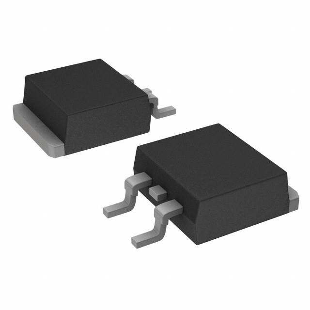
| 产品图片 |
|
| rohs | 符合RoHS无铅 / 符合限制有害物质指令(RoHS)规范要求 |
| 产品系列 | 晶体管,MOSFET,STMicroelectronics STF11NM60NDFDmesh™ II |
| 数据手册 | |
| 产品型号 | STF11NM60ND |
| Pd-PowerDissipation | 90 W |
| Pd-功率耗散 | 90 W |
| Qg-GateCharge | 30 nC |
| Qg-栅极电荷 | 30 nC |
| RdsOn-Drain-SourceResistance | 450 mOhms |
| RdsOn-漏源导通电阻 | 450 mOhms |
| Vds-Drain-SourceBreakdownVoltage | 600 V |
| Vds-漏源极击穿电压 | 600 V |
| Vgs-Gate-SourceBreakdownVoltage | 25 V |
| Vgs-栅源极击穿电压 | 25 V |
| Vgsth-Gate-SourceThresholdVoltage | 4 V |
| Vgsth-栅源极阈值电压 | 4 V |
| 上升时间 | 7 ns |
| 下降时间 | 9 ns |
| 不同Id时的Vgs(th)(最大值) | 5V @ 250µA |
| 不同Vds时的输入电容(Ciss) | 850pF @ 50V |
| 不同Vgs时的栅极电荷(Qg) | 30nC @ 10V |
| 不同 Id、Vgs时的 RdsOn(最大值) | 450 毫欧 @ 5A,10V |
| 产品种类 | MOSFET |
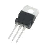
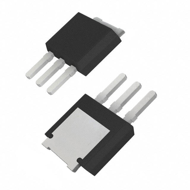
| 供应商器件封装 | TO-220FP |
| 其它名称 | 497-11884-5 |
| 其它有关文件 | http://www.st.com/web/catalog/sense_power/FM100/CL824/SC1167/PF211334?referrer=70071840 |
| 典型关闭延迟时间 | 50 ns |
| 功率-最大值 | 25W |
| 包装 | 管件 |
| 商标 | STMicroelectronics |
| 安装类型 | 通孔 |
| 安装风格 | Through Hole |
| 封装 | Tube |
| 封装/外壳 | TO-220-3 整包 |
| 封装/箱体 | TO-220FP-3 |
| 工厂包装数量 | 50 |
| 晶体管极性 | N-Channel |
| 最大工作温度 | + 150 C |
| 最小工作温度 | - 55 C |
| 标准包装 | 50 |
| 正向跨导-最小值 | 7.5 S |
| 漏源极电压(Vdss) | 600V |
| 电流-连续漏极(Id)(25°C时) | 10A (Tc) |
| 系列 | STF11NM60ND |
| 通道模式 | Enhancement |
| 配置 | Single |


PDF Datasheet 数据手册内容提取
STD11NM60ND, STF/I11NM60ND STP11NM60ND, STU11NM60ND Ω N-channel 600 V, 0.37 , 10 A, FDmesh™ II Power MOSFET 2 I PAK, TO-220, TO-220FP, IPAK, DPAK Features Order codes V (@T ) R max I DSS jmax DS(on) D 3 STD11NM60ND 10 A 1 123 STF11NM60ND 10 A(1) DPAK I²PAK STI11NM60ND 650 V < 0.45 Ω 10 A 3 STP11NM60ND 10 A 2 1 STU11NM60ND 10 A IPAK 1. Limited only by maximum temperature allowed ■ The worldwide best RDS(on)* area amongst the 123 123 fast recovery diode devices TO-220 TO-220FP ■ 100% avalanche tested ■ Low input capacitance and gate charge ■ Low gate input resistance ■ Extremely high dv/dt and avalanche capabilities Figure 1. Internal schematic diagram Application Switching applications (cid:36)(cid:8)(cid:18)(cid:9) Description The device is an N-channel FDmesh™ II Power MOSFET that belongs to the second generation (cid:39)(cid:8)(cid:17)(cid:9) of MDmesh™ technology. This revolutionary Power MOSFET associates a new vertical structure to the company's strip layout and associates all advantages of reduced on- (cid:51)(cid:8)(cid:19)(cid:9) resistance and fast switching with an intrinsic fast- recovery body diode.It is therefore strongly recommended for bridge topologies, in particular (cid:33)(cid:45)(cid:16)(cid:17)(cid:20)(cid:23)(cid:21)(cid:86)(cid:17) ZVS phase-shift converters. Table 1. Device summary Order codes Marking Package Packaging STD11NM60ND DPAK Tape and reel STF11NM60ND TO-220FP Tube STI11NM60ND 11NM60ND I2PAK Tube STP11NM60ND TO-220 Tube STU11NM60ND IPAK Tube October 2010 Doc ID 14625 Rev 2 1/19 www.st.com 19
Contents STD/F/I/P/U11NM60ND Contents 1 Electrical ratings . . . . . . . . . . . . . . . . . . . . . . . . . . . . . . . . . . . . . . . . . . . . 3 2 Electrical characteristics . . . . . . . . . . . . . . . . . . . . . . . . . . . . . . . . . . . . . 5 2.1 Electrical characteristics (curves) . . . . . . . . . . . . . . . . . . . . . . . . . . . . 7 3 Test circuits . . . . . . . . . . . . . . . . . . . . . . . . . . . . . . . . . . . . . . . . . . . . . 10 4 Package mechanical data . . . . . . . . . . . . . . . . . . . . . . . . . . . . . . . . . . . . 11 5 Packaging mechanical data . . . . . . . . . . . . . . . . . . . . . . . . . . . . . . . . . . 17 6 Revision history . . . . . . . . . . . . . . . . . . . . . . . . . . . . . . . . . . . . . . . . . . . 18 2/19 Doc ID 14625 Rev 2
STD/F/I/P/U11NM60ND Electrical ratings 1 Electrical ratings Table 2. Absolute maximum ratings Value Symbol Parameter Unit DPAK/I²PAK, TO-220FP TO-220/IPAK VDS Drain-source voltage (VGS=0) 600 V VGS Gate-source voltage ± 25 V ID Drain current (continuous) at TC = 25°C 10 10 (1) A ID Drain current (continuous) at TC = 100°C 6.3 6.3(1) A IDM (2) Drain current (pulsed) 40 40 (1) A PTOT Total dissipation at TC = 25°C 90 25 W dv/dt (3) Peak diode recovery voltage slope 40 V/ns Insulation withstand voltage (RMS) from all VISO three leads to external heat sink 2500 V (t=1s;T =25°C) C Tstg Storage temperature -55 to 150 °C Tj Max. operating junction temperature 150 °C 1. Limited only by maximum temperature allowed 2. Pulse width limited by safe operating area 3. I ≤ 10 A, di/dt ≤ 400 A/µs, V = 80% V , peak VDS ≤ V SD DD (BR)DSS (BR)DSS Table 3. Thermal data Value Symbol Parameter Unit TO-220 I²PAK DPAK IPAK TO-220FP Thermal resistance junction-case Rthj-case max 1.38 5 °C/W Rthj-amb Thermal resistance junction-amb max 62.5 100 62.5 °C/W R (1) Thermal resistance junction-pcb max 50 °C/W thj-pcb Maximum lead temperature for Tl soldering purposes 300 300 °C 1. When mounted on 1inch² FR-4 board, 2 oz Cu Doc ID 14625 Rev 2 3/19
Electrical ratings STD/F/I/P/U11NM60ND Table 4. Avalanche characteristics Symbol Parameter Max value Unit IAS Avalanche current, repetitive or not-repetitive(1) 3.5 A EAS Single pulse avalanche energy (2) 200 mJ 1. Pulse width limited by Tj max 2. starting Tj= 25 °C, I =I , V = 50 V D AS DD 4/19 Doc ID 14625 Rev 2
STD/F/I/P/U11NM60ND Electrical characteristics 2 Electrical characteristics (T = 25 °C unless otherwise specified) CASE Table 5. On/off states Symbol Parameter Test conditions Min. Typ. Max. Unit Drain-source breakdown V I = 1 mA, V = 0 600 V (BR)DSS voltage D GS V = 480 V,I = 10 A, dv/dt(1) Drain-source voltage slope DD D 45 V/ns V = 10 V GS I Zero gate voltage drain VDS = max rating, 1 µA DSS current (VGS = 0) VDS = max rating,@125 °C 100 µA Gate body leakage current I V = ±20 V 100 nA GSS (V = 0) GS DS V Gate threshold voltage V = V , I = 250 µA 3 4 5 V GS(th) DS GS D Static drain-source on R V = 10 V, I = 5 A 0.37 0.45 Ω DS(on) resistance GS D 1. Value measured at turn off under inductive load Table 6. Dynamic Symbol Parameter Test conditions Min. Typ. Max. Unit g (1) Forward transconductance V =15 V, I = 5 A - 7.5 - S fs DS D Input capacitance C 850 pF Ciss Output capacitance VDS = 50 V, f =1 MHz, - 44 - pF Coss Reverse transfer VGS = 0 5 pF rss capacitance Equivalent output C (2) V = 0, V = 0V to 480 V - 130 - pF oss eq. capacitance GS DS f=1 MHz Gate DC Bias=0 Rg Gate input resistance Test signal level=20 mV - 3.7 - Ω open drain Q Total gate charge V = 480 V, I = 10 A 30 nC g DD D Q Gate-source charge V = 10 V - 4 - nC gs GS Q Gate-drain charge (see Figure19) 16 nC gd 1. Pulsed: pulse duration = 300µs, duty cycle 1.5% 2. C is defined as a constant equivalent capacitance giving the same charging time as C when V oss eq. oss DS increases from 0 to 80% V DSS Doc ID 14625 Rev 2 5/19
Electrical characteristics STD/F/I/P/U11NM60ND Table 7. Switching times Symbol Parameter Test conditions Min Typ Max Unit t Turn-on delay time 16 ns d(on) V = 300 V, I = 5 A, t Rise time DD D 7 ns r R = 4.7 Ω, V = 10 V - - t Turn-off delay time G GS 50 ns d(off) (see Figure18) t Fall time 9 ns f Table 8. Source drain diode Symbol Parameter Test conditions Min Typ Max Unit I Source-drain current 10 A SD - I (1) Source-drain current (pulsed) 40 A SDM V (2) Forward on voltage I = 10 A, V =0 - 1.3 V SD SD GS trr Reverse recovery time ISD =10 A, di/dt =100 A/µs, 130 ns Qrr Reverse recovery charge VDD = 100 V - 0.69 µC I Reverse recovery current (see Figure20) 11 A RRM trr Reverse recovery time VDD = 100 V 200 ns Qrr Reverse recovery charge di/dt =100 A/µs, ISD = 10 A - 1.2 µC I Reverse recovery current Tj = 150 °C (see Figure20) 12 A RRM 1. Pulse width limited by safe operating area 2. Pulsed: pulse duration = 300µs, duty cycle 1.5% 6/19 Doc ID 14625 Rev 2
STD/F/I/P/U11NM60ND Electrical characteristics 2.1 Electrical characteristics (curves) Figure 2. Safe operating area for TO-220, Figure 3. Thermal impedance for TO-220, I²PAK I²PAK (cid:41)(cid:36) (cid:33)(cid:45)(cid:16)(cid:23)(cid:16)(cid:18)(cid:21)(cid:86)(cid:17) (cid:8)(cid:33)(cid:9) (cid:17)(cid:16) (cid:47)(cid:80)(cid:69)(cid:82)(cid:65)(cid:84)(cid:73)(cid:77)(cid:73)(cid:79)(cid:84)(cid:78)(cid:69)(cid:0)(cid:73)(cid:68)(cid:0)(cid:78)(cid:0)(cid:66)(cid:84)(cid:89)(cid:72)(cid:0)(cid:73)(cid:83)(cid:0)(cid:77)(cid:65)(cid:65)(cid:82)(cid:88)(cid:0)(cid:69)(cid:65)(cid:50)(cid:0)(cid:73)(cid:36)(cid:83)(cid:51)(cid:8)(cid:79)(cid:78)(cid:9) (cid:17)(cid:17)(cid:16)(cid:16)(cid:16)(cid:151)(cid:151)(cid:83)(cid:83) (cid:17) (cid:44)(cid:73) (cid:52)(cid:74)(cid:29)(cid:17)(cid:21)(cid:16)(cid:160)(cid:35) (cid:17)(cid:77)(cid:83) (cid:52)(cid:67)(cid:29)(cid:18)(cid:21)(cid:160)(cid:35) (cid:51)(cid:73)(cid:78)(cid:71)(cid:76)(cid:69) (cid:17)(cid:16)(cid:77)(cid:83) (cid:80)(cid:85)(cid:76)(cid:83)(cid:69) (cid:16)(cid:14)(cid:17) (cid:16)(cid:14)(cid:17) (cid:17) (cid:17)(cid:16) (cid:17)(cid:16)(cid:16) (cid:54)(cid:36)(cid:51)(cid:8)(cid:54)(cid:9) Figure 4. Safe operating area for TO-220FP Figure 5. Thermal impedance for TO-220FP ID AM08612v1 (A) 101 Operatmiitoen di nb ty hims aaxr eRa DiSs(on) 11000µµss Li 1ms Tj=150°C 10ms 0.1 Tc=25°C Single pulse 0.01 0.1 1 10 100 VDS(V) Figure 6. Safe operating area for DPAK, IPAK Figure 7. Thermal impedance for DPAK, IPAK ID AM08613v1 (A) 10µs 10 1 Operatimiotne id n btyh ism aarx eRa iDsS(on) 110m0sµs Li Tj=150°C 10ms Tc=25°C Single pulse 0.1 0.1 1 10 100 VDS(V) Doc ID 14625 Rev 2 7/19
Electrical characteristics STD/F/I/P/U11NM60ND Figure 8. Output characteristics Figure 9. Transfer characteristics Figure 10. Transconductance Figure 11. Static drain-source on resistance Figure 12. Gate charge vs gate-source voltage Figure 13. Capacitance variations 8/19 Doc ID 14625 Rev 2
STD/F/I/P/U11NM60ND Electrical characteristics Figure 14. Normalized gate threshold voltage Figure 15. Normalized on resistance vs vs temperature temperature Figure 16. Source-drain diode forward Figure 17. Normalized B vs temperature VDSS characteristics Doc ID 14625 Rev 2 9/19
Test circuits STD/F/I/P/U11NM60ND 3 Test circuits Figure 18. Switching times test circuit for Figure 19. Gate charge test circuit resistive load VDD 12V 47kΩ 1kΩ 100nF RL 2μ20F0 3μ.F3 VDD IG=CONST VD Vi=20V=VGMAX 100Ω D.U.T. VGS 2200 RG D.U.T. μF 2.7kΩ VG PW 47kΩ 1kΩ PW AM01468v1 AM01469v1 Figure 20. Test circuit for inductive load Figure 21. Unclamped inductive load test switching and diode recovery times circuit L A A A D FAST L=100μH VD G D.U.T. DIODE 2200 3.3 μF μF VDD S B 3.3 1000 B B μF μF 25Ω D VDD ID G RG S Vi D.U.T. Pw AM01470v1 AM01471v1 Figure 22. Unclamped inductive waveform Figure 23. Switching time waveform V(BR)DSS ton toff VD tdon tr tdoff tf 90% 90% IDM 10% ID 0 10% VDS VDD VDD 90% VGS AM01472v1 0 10% AM01473v1 10/19 Doc ID 14625 Rev 2
STD/F/I/P/U11NM60ND Package mechanical data 4 Package mechanical data In order to meet environmental requirements, ST offers these devices in different grades of ECOPACK® packages, depending on their level of environmental compliance. ECOPACK® specifications, grade definitions and product status are available at: www.st.com. ECOPACK is an ST trademark. Doc ID 14625 Rev 2 11/19
Package mechanical data STD/F/I/P/U11NM60ND Table 9. TO-220FP mechanical data mm Dim. Min. Typ. Max. A 4.4 4.6 B 2.5 2.7 D 2.5 2.75 E 0.45 0.7 F 0.75 1 F1 1.15 1.70 F2 1.15 1.70 G 4.95 5.2 G1 2.4 2.7 H 10 10.4 L2 16 L3 28.6 30.6 L4 9.8 10.6 L5 2.9 3.6 L6 15.9 16.4 L7 9 9.3 Dia 3 3.2 Figure 24. TO-220FP drawing L7 E A B D Dia L5 L6 F1 F2 F H G G1 L2 L4 L3 7012510_Rev_K 12/19 Doc ID 14625 Rev 2
STD/F/I/P/U11NM60ND Package mechanical data TO-220 type A mechanical data mm Dim Min Typ Max A 4.40 4.60 b 0.61 0.88 b1 1.14 1.70 c 0.48 0.70 D 15.25 15.75 D1 1.27 E 10 10.40 e 2.40 2.70 e1 4.95 5.15 F 1.23 1.32 H1 6.20 6.60 J1 2.40 2.72 L 13 14 L1 3.50 3.93 L20 16.40 L30 28.90 ∅P 3.75 3.85 Q 2.65 2.95 0015988_Rev_S Doc ID 14625 Rev 2 13/19
Package mechanical data STD/F/I/P/U11NM60ND I²PAK (TO-262) mechanical data mm inch Dim Min Typ Max Min Typ Max A 4.40 4.60 0.173 0.181 A1 2.40 2.72 0.094 0.107 b 0.61 0.88 0.024 0.034 b1 1.14 1.70 0.044 0.066 c 0.49 0.70 0.019 0.027 c2 1.23 1.32 0.048 0.052 D 8.95 9.35 0.352 0.368 e 2.40 2.70 0.094 0.106 e1 4.95 5.15 0.194 0.202 E 10 10.40 0.393 0.410 L 13 14 0.511 0.551 L1 3.50 3.93 0.137 0.154 L2 1.27 1.40 0.050 0.055 14/19 Doc ID 14625 Rev 2
STD/F/I/P/U11NM60ND Package mechanical data TO-252 (DPAK) mechanical data mm. DIM. min. typ max. A 2.20 2.40 A1 0.90 1.10 A2 0.03 0.23 b 0.64 0.90 b4 5.20 5.40 c 0.45 0.60 c2 0.48 0.60 D 6.00 6.20 D1 5.10 E 6.40 6.60 E1 4.70 e 2.28 e1 4.40 4.60 H 9.35 10.10 L 1 L1 2.80 L2 0.80 L4 0.60 1 R 0.20 V2 0 o 8o 0068772_G Doc ID 14625 Rev 2 15/19
Package mechanical data STD/F/I/P/U11NM60ND TO-251 (IPAK) mechanical data mm. DIM. min. typ max. A 2.20 2.40 A1 0.90 1.10 b 0.64 0.90 b2 0.95 b4 5.20 5.40 c 0.45 0.60 c2 0.48 0.60 D 6.00 6.20 E 6.40 6.60 e 2.28 e1 4.40 4.60 H 16.10 L 9.00 9.40 (L1) 0.80 1.20 L2 0.80 V1 10 o 0068771_H 16/19 Doc ID 14625 Rev 2
STD/F/I/P/U11NM60ND Packaging mechanical data 5 Packaging mechanical data DPAK FOOTPRINT All dimensions are in millimeters TAPE AND REEL SHIPMENT REEL MECHANICAL DATA mm inch DIM. MIN. MAX. MIN. MAX. A 330 12.992 B 1.5 0.059 C 12.8 13.2 0.504 0.520 D 20.2 0.795 G 16.4 18.4 0.645 0.724 N 50 1.968 T 22.4 0.881 BASE QTY BULK QTY TAPE MECHANICAL DATA 2500 2500 mm inch DIM. MIN. MAX. MIN. MAX. A0 6.8 7 0.267 0.275 B0 10.4 10.6 0.409 0.417 B1 12.1 0.476 D 1.5 1.6 0.059 0.063 D1 1.5 0.059 E 1.65 1.85 0.065 0.073 F 7.4 7.6 0.291 0.299 K0 2.55 2.75 0.100 0.108 P0 3.9 4.1 0.153 0.161 P1 7.9 8.1 0.311 0.319 P2 1.9 2.1 0.075 0.082 R 40 1.574 W 15.7 16.3 0.618 0.641 Doc ID 14625 Rev 2 17/19
Revision history STD/F/I/P/U11NM60ND 6 Revision history T able 10. Document revision history Date Revision Changes 23-Apr-2008 1 First release – Corrected Figure2: Safe operating area for TO-220, I²PAK 25-Oct-2010 2 – Corrected Figure4: Safe operating area for TO-220FP – Corrected Figure6: Safe operating area for DPAK, IPAK 18/19 Doc ID 14625 Rev 2
STD/F/I/P/U11NM60ND Please Read Carefully: Information in this document is provided solely in connection with ST products. STMicroelectronics NV and its subsidiaries (“ST”) reserve the right to make changes, corrections, modifications or improvements, to this document, and the products and services described herein at any time, without notice. All ST products are sold pursuant to ST’s terms and conditions of sale. Purchasers are solely responsible for the choice, selection and use of the ST products and services described herein, and ST assumes no liability whatsoever relating to the choice, selection or use of the ST products and services described herein. No license, express or implied, by estoppel or otherwise, to any intellectual property rights is granted under this document. If any part of this document refers to any third party products or services it shall not be deemed a license grant by ST for the use of such third party products or services, or any intellectual property contained therein or considered as a warranty covering the use in any manner whatsoever of such third party products or services or any intellectual property contained therein. UNLESS OTHERWISE SET FORTH IN ST’S TERMS AND CONDITIONS OF SALE ST DISCLAIMS ANY EXPRESS OR IMPLIED WARRANTY WITH RESPECT TO THE USE AND/OR SALE OF ST PRODUCTS INCLUDING WITHOUT LIMITATION IMPLIED WARRANTIES OF MERCHANTABILITY, FITNESS FOR A PARTICULAR PURPOSE (AND THEIR EQUIVALENTS UNDER THE LAWS OF ANY JURISDICTION), OR INFRINGEMENT OF ANY PATENT, COPYRIGHT OR OTHER INTELLECTUAL PROPERTY RIGHT. UNLESS EXPRESSLY APPROVED IN WRITING BY AN AUTHORIZED ST REPRESENTATIVE, ST PRODUCTS ARE NOT RECOMMENDED, AUTHORIZED OR WARRANTED FOR USE IN MILITARY, AIR CRAFT, SPACE, LIFE SAVING, OR LIFE SUSTAINING APPLICATIONS, NOR IN PRODUCTS OR SYSTEMS WHERE FAILURE OR MALFUNCTION MAY RESULT IN PERSONAL INJURY, DEATH, OR SEVERE PROPERTY OR ENVIRONMENTAL DAMAGE. ST PRODUCTS WHICH ARE NOT SPECIFIED AS "AUTOMOTIVE GRADE" MAY ONLY BE USED IN AUTOMOTIVE APPLICATIONS AT USER’S OWN RISK. Resale of ST products with provisions different from the statements and/or technical features set forth in this document shall immediately void any warranty granted by ST for the ST product or service described herein and shall not create or extend in any manner whatsoever, any liability of ST. ST and the ST logo are trademarks or registered trademarks of ST in various countries. Information in this document supersedes and replaces all information previously supplied. The ST logo is a registered trademark of STMicroelectronics. All other names are the property of their respective owners. © 2010 STMicroelectronics - All rights reserved STMicroelectronics group of companies Australia - Belgium - Brazil - Canada - China - Czech Republic - Finland - France - Germany - Hong Kong - India - Israel - Italy - Japan - Malaysia - Malta - Morocco - Philippines - Singapore - Spain - Sweden - Switzerland - United Kingdom - United States of America www.st.com Doc ID 14625 Rev 2 19/19
Mouser Electronics Authorized Distributor Click to View Pricing, Inventory, Delivery & Lifecycle Information: S TMicroelectronics: STP11NM60ND STD11NM60ND STF11NM60ND STI11NM60ND STU11NM60ND