首页 > IXFH26N50P > 详情
 Datasheet下载
- 型号: IXFH26N50P
- 制造商: IXYS
- 库位|库存: xxxx|xxxx
- 要求:
| 数量阶梯 | 香港交货 | 国内含税 |
| +xxxx | $xxxx | ¥xxxx |
查看当月历史价格
查看今年历史价格
产品参数
| 参数 | 数值 |
| 产品目录 | 分立半导体产品半导体 |
| ChannelMode | Enhancement |
| 描述 | MOSFET N-CH 500V 26A TO-247MOSFET HiPERFET Id26 BVdass500 |
| 产品分类 | FET - 单分离式半导体 |
| FET功能 | 标准 |
| FET类型 | MOSFET N 通道,金属氧化物 |
| Id-ContinuousDrainCurrent | 26 A |
| Id-连续漏极电流 | 26 A |
| 品牌 | IXYS |
| 产品手册 | 点击此处下载产品Datasheet |
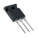
| 产品图片 |   |
| rohs | 符合RoHS无铅 / 符合限制有害物质指令(RoHS)规范要求 |
| 产品系列 | 晶体管,MOSFET,IXYS IXFH26N50PPolarHV™ HiPerFET™ |
| 数据手册 | 点击此处下载产品Datasheet |
| 产品型号 | IXFH26N50P |
| Pd-PowerDissipation | 400 W |
| Pd-功率耗散 | 400 W |
| RdsOn-Drain-SourceResistance | 230 mOhms |
| RdsOn-漏源导通电阻 | 230 mOhms |
| Vds-Drain-SourceBreakdownVoltage | 500 V |
| Vds-漏源极击穿电压 | 500 V |
| Vgs-Gate-SourceBreakdownVoltage | +/- 30 V |
| Vgs-栅源极击穿电压 | 30 V |
| 上升时间 | 25 ns |
| 下降时间 | 20 ns |
| 不同Id时的Vgs(th)(最大值) | 5.5V @ 4mA |
| 不同Vds时的输入电容(Ciss) | 3600pF @ 25V |
| 不同Vgs时的栅极电荷(Qg) | 60nC @ 10V |
| 不同 Id、Vgs时的 RdsOn(最大值) | 230 毫欧 @ 13A,10V |
| 产品种类 | MOSFET |
| 供应商器件封装 | TO-247AD (IXFH) |
| 典型关闭延迟时间 | 58 ns |
| 功率-最大值 | 400W |
| 包装 | 管件 |
| 单位重量 | 6.500 g |
| 商标 | IXYS |
| 商标名 | HiPerFET |
| 安装类型 | 通孔 |
| 安装风格 | Through Hole |
| 封装 | Tube |
| 封装/外壳 | TO-247-3 |
| 封装/箱体 | TO-247-3 |
| 工厂包装数量 | 30 |
| 晶体管极性 | N-Channel |
| 最大工作温度 | + 150 C |
| 最小工作温度 | - 55 C |
| 标准包装 | 30 |
| 正向跨导-最小值 | 26 S |
| 漏源极电压(Vdss) | 500V |
| 电流-连续漏极(Id)(25°C时) | 26A (Tc) |
| 系列 | IXFH26N50 |
| 通道模式 | Enhancement |
| 配置 | Single |
Datasheet
PDF Datasheet 数据手册内容提取
PolarHVTM HiPerFET IXFH 26N50P V = 500 V DSS IXFV 26N50P I = 26 A Power MOSFET D25 ≤≤≤≤≤ ΩΩΩΩΩ IXFV 26N50PS R 230 m DS(on) ≤≤≤≤≤ N-Channel Enhancement Mode t 200 ns rr Avalanche Rated Fast Intrinsic Diode Symbol Test Conditions Maximum Ratings V T = 25°C to 150°C 500 V DSS J V T = 25°C to 150°C; R = 1 MΩ 500 V TO-247 (IXFH) DGR J GS V Continuos ± 30 V GSS V Transient ± 40 V GSM I T = 25°C 26 A D25 C I T = 25°C, pulse width limited by T 78 A DM C JM D (TAB) I T = 25°C 26 A AR C E T = 25°C 40 mJ AR C E T = 25°C 1.0 J PLUS220 (IXFV) AS C dv/dt I ≤ I , di/dt ≤ 100 A/µs, V ≤ V , 10 V/ns S DM DD DSS T ≤ 150°C, R = 4 Ω J G P T = 25°C 400 W G D C D D (TAB) T -55 ... +150 °C S J T 150 °C JM T -55 ... +150 °C PLUS220SMD (IXFV_S) stg T 1.6 mm (0.062 in.) from case for 10 s 300 °C L T Plastic body for 10 s 260 °C SOLD M Mounting torque (TO-247) 1.13/10 Nm/lb.in. d F Mounting force (PLUS220) 11..65/2.5..15 N/lb G C S D (TAB) Weight TO-247 6 g PLUS220 & PLUS220SMD 5 g G = Gate D = Drain S = Source TAB = Drain Features Symbol Test Conditions Characteristic Values l International standard packages (TJ = 25°C, unless otherwise specified) Min. Typ. Max. l Fast intrinsic diode BV V = 0 V, I = 250 µA 500 V l Unclamped Inductive Switching (UIS) DSS GS D rated V V = V , I = 4 mA 3.0 5.5 V l Low package inductance GS(th) DS GS D - easy to drive and to protect I V = ±30 V , V = 0 ±100 nA GSS GS DC DS Advantages I V = V 25 µA DSS DS DSS l Easy to mount V = 0 V T = 125°C 250 µA GS J l Space savings R V = 10 V, I = 0.5 I 230 mΩ l High power density DS(on) GS D D25 Pulse test, t ≤ 300 µs, duty cycle d ≤ 2 % © 2006 IXYS All rights reserved DS99276E(12/05)
IXFH 26N50P IXFV 26N50P IXFV 26N50PS Symbol Test Conditions Characteristic Values (T = 25°C, unless otherwise specified) TO-247 AD (IXFH) Outline J Min. Typ. Max. g V = 20 V; I = 0.5 I , pulse test 16 26 S fs DS D D25 C 3600 pF iss C V = 0 V, V = 25 V, f = 1 MHz 370 pF 1 2 3 Terminals: oss GS DS 1 - Gate C 40 pF 2 - Drain rss 3 - Source Tab - Drain t 20 ns d(on) t V = 10 V, V = 0.5 I 25 ns r GS DS D25 t R = 4 Ω (External) 58 ns d(off) G t 20 ns Dim. Millimeter Inches f Min. Max. Min. Max. Q 60 nC A 4.7 5.3 .185 .209 g(on) A 2.2 2.54 .087 .102 1 Q V = 10 V, V = 0.5 V , I = 0.5 I 20 nC A2 2.2 2.6 .059 .098 gs GS DS DSS D D25 b 1.0 1.4 .040 .055 Q 25 nC b 1.65 2.13 .065 .084 gd 1 b 2.87 3.12 .113 .123 2 R 0.31 °C/W C .4 .8 .016 .031 thJC D 20.80 21.46 .819 .845 R (TO-247, PLUS220) 0.21 °C/W E 15.75 16.26 .610 .640 thCS e 5.20 5.72 0.205 0.225 L 19.81 20.32 .780 .800 L1 4.50 .177 Source-Drain Diode Characteristic Values (T = 25°C, unless otherwise specified) ∅P 3.55 3.65 .140 .144 J Q 5.89 6.40 0.232 0.252 Symbol Test Conditions Min. Typ. Max. R 4.32 5.49 .170 .216 S 6.15 BSC 242 BSC I V = 0 V 26 A S GS I Repetitive 104 A SM PLUS220 (IXFV) Outline V I = I , V = 0 V, 1.5 V SD F S GS Pulse test, t ≤ 300 µs, duty cycle d ≤ 2 % t I = 25A, -di/dt = 100 A/µs 200 ns rr F Q V = 100V, V = 0 V 0.6 µC RM R GS I 6 Α RM PLUS220SMD (IXFV_S) Outline IXYS reserves the right to change limits, test conditions, and dimensions. IXYS MOSFETs and IGBTs are covered by4,835,592 4,931,844 5,049,961 5,237,481 6,162,665 6,404,065 B1 6,683,344 6,727,585 one or moreof the following U.S. patents: 4,850,072 5,017,508 5,063,307 5,381,025 6,259,123 B1 6,534,343 6,710,405B2 6,759,692 4,881,106 5,034,796 5,187,117 5,486,715 6,306,728 B1 6,583,505 6,710,463 6,771,478 B2
IXFH 26N50P IXFV 26N50P IXFV 26N50PS Fig. 1. Output Characteristics Fig. 2. Extended Output Characteristics @ 25ºC @ 25ºC 26 60 24 VGS = 10V 55 VGS = 10V 8V 8V 22 7V 50 20 45 18 40 7V peres 1146 peres 35 m m 30 A 12 A - D 10 6V - D 25 I I 20 8 6V 6 15 4 10 2 5V 5 5V 0 0 0 1 2 3 4 5 6 7 0 3 6 9 12 15 18 21 24 27 30 VDS - Volts VDS - Volts Fig. 3. Output Characteristics Fig. 4. RDS(on) Normalized to ID = 13A Value @ 125ºC vs. Junction Temperature 26 3.1 24 V G S = 1 70VV 2.8 VGS = 10V 22 20 2.5 d 18 6V ze 2.2 es 16 ali per 14 orm 1.9 I D = 26A m N I - AD 11028 R - DS(on) 11..36 I D = 13A 6 5V 1 4 0.7 2 0 0.4 0 2 4 6 8 10 12 14 16 -50 -25 0 25 50 75 100 125 150 V - Volts T - Degrees Centigrade DS J Fig. 5. RDS(on) Normalized to ID = 13A Value Fig. 6. Maximum Drain Current vs. vs. Drain Current Case Temperature 3.2 30 3 VGS = 10V 2.8 TJ = 125ºC 25 2.6 d e z 2.4 20 ali es orm 2.2 per N 2 m 15 - DS(on) 11..68 I - AD 10 R 1.4 1.2 TJ = 25ºC 5 1 0.8 0 0 5 10 15 20 25 30 35 40 45 50 55 60 -50 -25 0 25 50 75 100 125 150 ID - Amperes TJ - Degrees Centigrade © 2006 IXYS All rights reserved
IXFH 26N50P IXFV 26N50P IXFV 26N50PS Fig. 7. Input Admittance Fig. 8. Transconductance 50 50 45 45 40 40 35 35 TJ = - 40ºC mperes 2350 T J = 1 2255ººCC Siemens 2350 1 2255ººCC I - AD 20 - 40ºC g - f s 20 15 15 10 10 5 5 0 0 3.5 4 4.5 5 5.5 6 6.5 7 0 5 10 15 20 25 30 35 40 45 50 55 60 V - Volts I - Amperes GS D Fig. 9. Forward Voltage Drop of Intrinsic Diode Fig. 10. Gate Charge 80 10 9 VDS = 250V 70 I D = 13A 8 60 I G = 10mA 7 eres 50 olts 6 p V Am 40 - S 5 I - S 30 TJ = 125ºC VG 4 3 20 2 10 TJ = 25ºC 1 0 0 0.4 0.5 0.6 0.7 0.8 0.9 1 1.1 0 5 10 15 20 25 30 35 40 45 50 55 60 65 V - Volts Q - NanoCoulombs SD G Fig. 11. Capacitance Fig. 12. Forward-Bias Safe Operating Area 10,000 100 f = 1 MHz RDS(on) Limit s Ciss ad 25µs ance - PicoFar1,000 Coss - AmperesD10 11m00sµs acit 100 I 10ms p a C DC TJ = 150ºC Crss TC = 25ºC 10 1 0 5 10 15 20 25 30 35 40 10 100 1000 V - Volts V - Volts DS DS IXYS reserves the right to change limits, test conditions, and dimensions.
IXFH 26N50P IXFV 26N50P IXFV 26N50PS Fig. 13. Maximum Transient Thermal Resistance 1.000 W C / - º 0.100 C J h) R(t 0.010 0.0001 0.001 0.01 0.1 1 10 Pulse Width - Seconds © 2006 IXYS All rights reserved
Disclaimer Notice - Information furnished is believed to be accurate and reliable. However, users should independently evaluate the suitability of and test each product selected for their own applications. Littelfuse products are not designed for, and may not be used in, all applications.Read complete Disclaimer Notice at www.littelfuse.com/disclaimer-electronics.