ICGOO在线商城 > 分立半导体产品 > 晶体管 - FET,MOSFET - 阵列 > SI4816BDY-T1-GE3
 Datasheet下载
- 型号: SI4816BDY-T1-GE3
- 制造商: Vishay
- 库位|库存: xxxx|xxxx
- 要求:
| 数量阶梯 | 香港交货 | 国内含税 |
| +xxxx | $xxxx | ¥xxxx |
查看当月历史价格
查看今年历史价格
SI4816BDY-T1-GE3产品简介:
ICGOO电子元器件商城为您提供SI4816BDY-T1-GE3由Vishay设计生产,在icgoo商城现货销售,并且可以通过原厂、代理商等渠道进行代购。 SI4816BDY-T1-GE3价格参考。VishaySI4816BDY-T1-GE3封装/规格:晶体管 - FET,MOSFET - 阵列, 2 个 N 通道(半桥) Mosfet 阵列 30V 5.8A,8.2A 1W,1.25W 表面贴装 8-SO。您可以下载SI4816BDY-T1-GE3参考资料、Datasheet数据手册功能说明书,资料中有SI4816BDY-T1-GE3 详细功能的应用电路图电压和使用方法及教程。
Vishay Siliconix的SI4816BDY-T1-GE3是一款双N沟道MOSFET阵列,广泛应用于各种需要高效开关和低导通电阻的电路中。以下是其主要应用场景:

 1. 电源管理
   - DC-DC转换器:该器件适用于降压、升压或升降压转换器中的同步整流应用。双MOSFET结构可以分别用作高边和低边开关,提高效率并减少功率损耗。
   - 负载开关:在便携式设备(如智能手机、平板电脑)中,用于控制不同负载的供电路径,确保快速响应和低功耗。

 2. 电机驱动
   - H桥电路:在小型电机驱动中,SI4816BDY-T1-GE3可以用作H桥的上下桥臂,实现电机的正反转控制。其低导通电阻有助于降低发热,延长电机寿命。
   - 步进电机控制:在精密控制应用中,如打印机、扫描仪等设备,该器件可以提供稳定的电流输出,确保电机运行平稳。

 3. 信号切换
   - 多路复用器/解复用器:在需要频繁切换信号路径的应用中,如音频切换、传感器信号处理等,该MOSFET阵列可以实现快速、低损耗的信号切换。
   - 数据通信接口保护:用于USB、HDMI等高速接口的过流保护和ESD防护,确保信号完整性的同时提供必要的保护功能。

 4. 电池管理系统
   - 电池充放电控制:在锂电池管理系统中,该器件可以作为充放电路径的开关,防止过充、过放及短路等异常情况。
   - 电量监测:配合电流检测电阻,用于实时监测电池的充放电电流,确保电池工作在安全范围内。

 5. 消费电子
   - 智能家电:如智能音箱、智能家居控制器等设备中,用于电源管理和信号切换,确保设备的稳定性和可靠性。
   - 游戏机与外设:用于手柄、耳机等外设的电源控制和信号传输,提升用户体验。

总之,SI4816BDY-T1-GE3凭借其低导通电阻、快速开关特性和紧凑封装,非常适合应用于对效率、可靠性和空间有较高要求的场景。
| 参数 | 数值 |
| 产品目录 | |
| ChannelMode | Enhancement |
| 描述 | MOSFET 2N-CH 30V 5.8A 8-SOICMOSFET Dua lN-Ch w/Schottky 30V 18.5/11.5mohm |
| 产品分类 | FET - 阵列分离式半导体 |
| FET功能 | 逻辑电平门 |
| FET类型 | 2 个 N 通道(半桥) |
| Id-ContinuousDrainCurrent | 5.8 A |
| Id-连续漏极电流 | 5.8 A |
| 品牌 | Vishay / SiliconixVishay Siliconix |
| 产品手册 | http://www.vishay.com/doc?73026 |
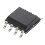
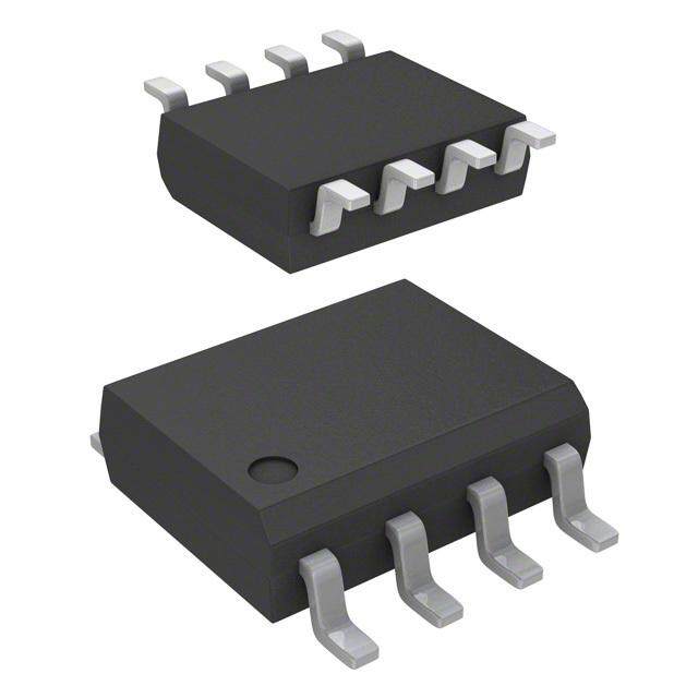
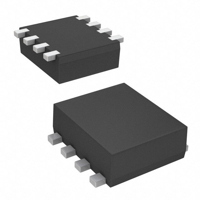
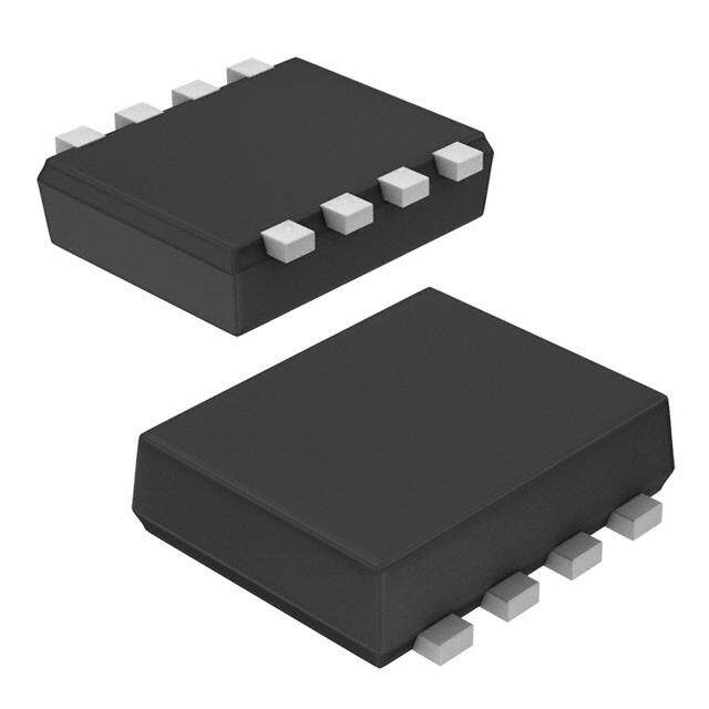
| 产品图片 |
|
| rohs | 符合RoHS无铅 / 符合限制有害物质指令(RoHS)规范要求 |
| 产品系列 | 晶体管,MOSFET,Vishay / Siliconix SI4816BDY-T1-GE3LITTLE FOOT® |
| 数据手册 | |
| 产品型号 | SI4816BDY-T1-GE3SI4816BDY-T1-GE3 |
| Pd-PowerDissipation | 1 W, 1.25 W |
| Pd-功率耗散 | 1 W, 1.25 W |
| RdsOn-Drain-SourceResistance | 15.5 mOhms, 9.3 mOhms |
| RdsOn-漏源导通电阻 | 15.5 mOhms, 9.3 mOhms |
| Vds-Drain-SourceBreakdownVoltage | 30 V |
| Vds-漏源极击穿电压 | 30 V |
| Vgs-Gate-SourceBreakdownVoltage | 20 V |
| Vgs-栅源极击穿电压 | 20 V |
| 上升时间 | 9 ns |
| 下降时间 | 9 ns |
| 不同Id时的Vgs(th)(最大值) | 3V @ 250µA |
| 不同Vds时的输入电容(Ciss) | - |
| 不同Vgs时的栅极电荷(Qg) | 10nC @ 5V |
| 不同 Id、Vgs时的 RdsOn(最大值) | 18.5 毫欧 @ 6.8A,10V |
| 产品目录页面 | |
| 产品种类 | MOSFET |
| 供应商器件封装 | 8-SO |
| 其它名称 | SI4816BDY-T1-GE3TR |
| 典型关闭延迟时间 | 24 ns, 31 ns |
| 功率-最大值 | 1W,1.25W |
| 包装 | 带卷 (TR) |
| 商标 | Vishay / Siliconix |
| 安装类型 | 表面贴装 |
| 安装风格 | SMD/SMT |
| 封装 | Reel |
| 封装/外壳 | 8-SOIC(0.154",3.90mm 宽) |
| 封装/箱体 | SOIC-8 Narrow |
| 工厂包装数量 | 2500 |
| 晶体管极性 | N-Channel |
| 最大工作温度 | + 150 C |
| 最小工作温度 | - 55 C |
| 标准包装 | 2,500 |
| 漏源极电压(Vdss) | 30V |
| 电流-连续漏极(Id)(25°C时) | 5.8A,8.2A |
| 通道模式 | Enhancement |
| 配置 | Dual with Schottky Diode |
| 零件号别名 | SI4816DY-T1-E3-S |


PDF Datasheet 数据手册内容提取
Si4816BDY Vishay Siliconix Dual N-Channel 30-V (D-S) MOSFET with Schottky Diode FEATURES PRODUCT SUMMARY • Halogen-free According to IEC 61249-2-21 V (V) R (Ω) I (A) Q (Typ.) DS DS(on) D g Available Channel-1 0.0185 at VGS = 10 V 6.8 7.8 (cid:129) LITTLE FOOT® Plus Power MOSFET 0.0225 at VGS = 4.5 V 6.0 (cid:129) 100 % R Tested 30 g 0.0115 at VGS = 10 V 11.4 Channel-2 11.6 0.016 at VGS = 4.5 V 9.5 SCHOTTKY PRODUCT SUMMARY VSD (V) D1 VDS (V) Diode Forward Voltage IF (A) 30 0.50 V at 1.0 A 2.0 SO-8 G1 G1 1 8 D1 N-Channel 1 A/S2 2 7 D2/S1 MOSFET S1/D2 A/S2 3 6 D2/S1 G2 4 5 D2/S1 Schottky Diode G2 Top View N-Channel 2 Ordering Information:Si4816BDY-T1-E3 (Lead (Pb)-free) MOSFET Si4816BDY-T1-GE3 (Lead (Pb)-free and Halogen-free) S2 A ABSOLUTE MAXIMUM RATINGS T = 25 °C, unless otherwise noted A Channel-1 Channel-2 Parameter Symbol 10 s Steady State 10 s Steady State Unit Drain-Source Voltage VDS 30 V Gate-Source Voltage VGS 20 Continuous Drain Current (TJ = 150 °C)a TTAA == 2750 °°CC ID 65..85 54..86 191.0.4 86..25 Pulsed Drain Current IDM 30 40 A Continuous Source Current (Diode Conduction)a IS 1 0.9 2.2 1.15 Single Pulse Avalanche Current IAS 10 20 L = 0.1 mH Avalanche Energy EAS 5 20 mJ TA = 25 °C 1.4 1.0 2.4 1.25 Maximum Power Dissipationa PD W TA = 70 °C 0.9 0.64 1.5 0.8 Operating Junction and Storage Temperature Range TJ, Tstg - 55 to 150 °C THERMAL RESISTANCE RATINGS Channel-1 Channel-2 Schottky Parameter Symbol Typ. Max. Typ. Max. Typ. Max. Unit t ≤ 10 s 72 90 43 53 48 60 Maximum Junction-to-Ambienta RthJA Steady State 100 125 82 100 80 100 °C/W Maximum Junction-to-Foot (Drain) Steady State RthJF 51 63 25 30 28 35 Notes: a. Surface Mounted on 1" x 1" FR4 board. Document Number: 73026 www.vishay.com S09-0394-Rev. D, 09-Mar-09 1
Si4816BDY Vishay Siliconix MOSFET SPECIFICATIONS T = 25 °C, unless otherwise noted J Parameter Symbol Test Conditions Min. Typ.a Max. Unit Static Ch-1 1.0 3.0 Gate Threshold Voltage VGS(th) VDS = VGS, ID = 250 µA V Ch-2 1.0 3.0 Ch-1 100 Gate-Body Leakage IGSS VDS = 0 V, VGS = 20 V nA Ch-2 100 Ch-1 1 V = 30 V, V = 0 V DS GS Ch-2 100 Zero Gate Voltage Drain Current IDSS µA Ch-1 15 V = 30 V, V = 0 V, T = 85 °C DS GS J Ch-2 2000 Ch-1 20 On-State Drain Currentb ID(on) VDS = 5 V, VGS = 10 V A Ch-2 30 VGS = 10 V, ID = 6.8 A Ch-1 0.0155 0.0185 VGS = 10 V, ID = 11.4 A Ch-2 0.0093 0.0115 Drain-Source On-State Resistanceb RDS(on) Ω VGS = 4.5 V, ID = 6.0 A Ch-1 0.0185 0.0225 VGS = 4.5 V, ID = 9.5 A Ch-2 0.013 0.016 VDS = 15 V, ID = 6.8 A Ch-1 30 Forward Transconductanceb gfs S VDS = 15 V, ID = 11.4 A Ch-2 31 IS = 1 A, VGS = 0 V Ch-1 0.73 1.1 Diode Forward Voltageb VSD V IS = 1 A, VGS = 0 V Ch-2 0.47 0.5 Dynamica Ch-1 7.8 10 Total Gate Charge Qg Channel-1 Ch-2 11.6 18 V = 15 V, V = 5 V, I = 6.8 A DS GS D Ch-1 2.9 Gate-Source Charge Qgs nC Ch-2 4.8 Channel-2 V = 15 V, V = 5 V, I = - 11.4 A Ch-1 2.3 Gate-Drain Charge Qgd DS GS D Ch-2 3.7 Ch-1 1.5 3.0 4.5 Gate Resistance Rg Ω Ch-2 0.9 1.8 2.7 Ch-1 11 17 Turn-On Delay Time td(on) Channel-1 Ch-2 13 20 V = 15 V, R = 15 Ω DD L Ch-1 9 15 Rise Time tr ID ≅ 1 A, VGEN = 10 V, Rg = 6 Ω Ch-2 9 15 Ch-1 24 40 Turn-Off Delay Time td(off) Channel-2 ns V = 15 V, R = 15 Ω Ch-2 31 50 DD L I ≅ 1 A, V = 10 V, R = 6 Ω Ch-1 9 15 Fall Time tf D GEN g Ch-2 11 17 IF = 1.3 A, dI/dt = 100 A/µs Ch-1 20 35 Source-Drain Reverse Recovery Time trr IF = 2.2 A, dI/dt = 100 µA/µs Ch-2 25 40 Notes: a. Guaranteed by design, not subject to production testing. b. Pulse test; pulse width ≤ 300 µs, duty cycle ≤ 2 %. www.vishay.com Document Number: 73026 2 S09-0394-Rev. D, 09-Mar-09
Si4816BDY Vishay Siliconix SCHOTTKY SPECIFICATIONS T = 25 °C, unless otherwise noted J Parameter Symbol Test Conditions Min. Typ. Max. Unit IF = 1.0 A 0.47 0.50 Forward Voltage Drop VF V IF = 1.0 A, TJ = 125 °C 0.36 0.42 VR = 30 V 0.004 0.100 Maximum Reverse Leakage Current Irm VR = 30 V, TJ = 100 °C 0.7 10 mA VR = - 30 V, TJ = 125 °C 3.0 20 Junction Capacitance CT VR = 10 V 50 pF Stresses beyond those listed under “Absolute Maximum Ratings” may cause permanent damage to the device. These are stress ratings only, and functional operation of the device at these or any other conditions beyond those indicated in the operational sections of the specifications is not implied. Exposure to absolute maximum rating conditions for extended periods may affect device reliability. CHANNEL-1 TYPICAL CHARACTERISTICS 25°C, unless otherwise noted 40 40 35 VGS = 10 thru 4 V 35 30 30 A) A) nt ( 25 nt ( 25 e e urr urr C C n 20 n 20 ai ai Dr Dr – 15 – 15 D D TC = 125 °C I 10 I 10 3 V 5 5 25 °C 2 V - 55 °C 0 0 0 1 2 3 4 5 0.0 0.5 1.0 1.5 2.0 2.5 3.0 3.5 4.0 4.5 VDS – Drain-to-Source Voltage (V) VGS – Gate-to-Source Voltage (V) Output Characteristics Transfer Characteristics 0.05 1200 0.04 1000 Ciss )Ω F) esistance ( 0.03 acitance (p 800 n-R VGS = 4.5 V Cap 600 – On) 0.02 C – 400 DS(o VGS = 10 V Coss R 0.01 200 Crss 0.00 0 0 5 10 15 20 25 30 35 40 0 5 10 15 20 25 30 ID – Drain Current (A) VDS – Drain-to-Source Voltage (V) On-Resistance vs. Drain Current Capacitance Document Number: 73026 www.vishay.com S09-0394-Rev. D, 09-Mar-09 3
Si4816BDY Vishay Siliconix CHANNEL-1 TYPICAL CHARACTERISTICS 25°C, unless otherwise noted 6 1.6 e (V) 5 VIDD =S 6=. 81 5A V 1.4 VIDG =S 6=. 81 0A V g a e Volt 4 ance – Gate-to-Sourc 23 – On-ResistS(on)(Normalized) 11..02 GS RD V 0.8 1 0 0.6 0 2 4 6 8 10 -50 -25 0 25 50 75 100 125 150 Qg – Total Gate Charge (nC) TJ – Junction Temperature (°C) Gate Charge On-Resistance vs. Junction Temperature 40 0.05 )Ω 0.04 ent (A) 10 TJ = 150 °C ance ( e Curr Resist 0.03 ID = 6.8 A – Sourc TJ = 25 °C – On-n) 0.02 IS DS(o R 0.01 1 0.00 0.0 0.2 0.4 0.6 0.8 1.0 1.2 1.4 0 2 4 6 8 10 VSD – Source-to-Drain Voltage (V) VGS – Gate-to-Source Voltage (V) Source-Drain Diode Forward Voltage On-Resistance vs. Gate-to-Source Voltage 0.4 100 0.2 80 ID = 250 µA V) e ( 0.0 anc W) 60 Vari -0.2 er ( S(th) Pow 40 G V -0.4 20 -0.6 -0.8 0 -50 -25 0 25 50 75 100 125 150 0.001 0.01 0.1 1 10 TJ – Temperature (°C) Time (s) Threshold Voltage Single Pulse Power, Junction-to-Ambient www.vishay.com Document Number: 73026 4 S09-0394-Rev. D, 09-Mar-09
Si4816BDY Vishay Siliconix CHANNEL-1 TYPICAL CHARACTERISTICS 25°C, unless otherwise noted 100 Limited by RDS(on )* IDM Limited 10 A) nt ( 1 ms e Curr 1 ID(on) 10 ms n Limited ai Dr – 100 ms ID 0.1 STinCg =le 2P5u °lsCe 1 s 10 s DC BVDSS Limited 0.01 0.1 1 10 100 VDS – Drain-to-Source Voltage (V) * VGS > minimum VGS at which RDS(on) is specified Safe Operating Area 2 1 nt Duty Cycle = 0.5 e e Transiedance 0.2 ctivmp Notes: ed Effeermal I 0.1 0.1 PDM malizTh 0.05 t1 Nor 0.02 1. Duty Cyclet,2 D = t1 t2 2. Per Unit Base = RthJA = 100°C/W 3. TJM - TA = PDMZthJA(t) Single Pulse 4. Surface Mounted 0.01 10-4 10-3 10-2 10-1 1 10 100 600 Square Wave Pulse Duration (s) Normalized Thermal Transient Impedance, Junction-to-Ambient 2 1 nt Duty Cycle = 0.5 e e Transiedance 0.2 ctivmp ed Effeermal I 0.1 0.1 alizTh 0.05 m or 0.02 N Single Pulse 0.01 10-4 10-3 10-2 10-1 1 10 Square Wave Pulse Duration (s) Normalized Thermal Transient Impedance, Junction-to-Foot Document Number: 73026 www.vishay.com S09-0394-Rev. D, 09-Mar-09 5
Si4816BDY Vishay Siliconix CHANNEL-2 TYPICAL CHARACTERISTICS 25°C, unless otherwise noted 40 40 VGS = 10 thru 5 V 32 32 A) 4 V A) Current ( 24 Current ( 24 Drain 16 Drain 16 – – D D TC = 125 °C I I 8 8 25 °C 3 V 2 V - 55 °C 0 0 0 1 2 3 4 5 0.0 0.5 1.0 1.5 2.0 2.5 3.0 3.5 4.0 4.5 VDS – Drain-to-Source Voltage (V) VGS – Gate-to-Source Voltage (V) Output Characteristics Transfer Characteristics 0.020 2000 Ciss e ()Ω 0.016 VGS = 4.5 V pF) 1600 Resistanc 0.012 VGS = 10 V acitance ( 1200 – On- 0.008 – Cap 800 n) C S(o Coss RD 0.004 400 Crss 0.000 0 0 5 10 15 20 25 30 0 6 12 18 24 30 ID – Drain Current (A) VDS – Drain-to-Source Voltage (V) On-Resistance vs. Drain Current Capacitance 6 1.6 e (V) 5 VIDD =S 9=. 51 5A V 1.4 VIDG =S 9=. 51 0A V g Volta 4 ance urce esist zed) 1.2 Gate-to-So 23 – On-Ron)(Normali 1.0 – DS( R S G 0.8 V 1 0 0.6 0 3 6 9 12 15 -50 -25 0 25 50 75 100 125 150 Qg – Total Gate Charge (nC) TJ – Junction Temperature (°C) Gate Charge On-Resistance vs. Junction Temperature www.vishay.com Document Number: 73026 6 S09-0394-Rev. D, 09-Mar-09
Si4816BDY Vishay Siliconix CHANNEL-2 TYPICAL CHARACTERISTICS 25°C, unless otherwise noted 40 0.05 0.04 ent (A) 10 TJ = 150 °C nce ()Ω ce Curr Resista 0.03 – SourS TJ = 25 °C – On-on) 0.02 ID = 9.5 A I S( RD 0.01 1 0.00 0.0 0.2 0.4 0.6 0.8 1.0 1.2 1.4 0 2 4 6 8 10 VSD – Source-to-Drain Voltage (V) VGS – Gate-to-Source Voltage (V) Source-Drain Diode Forward Voltage On-Resistance vs. Gate-to-Source Voltage 10 100 11 80 A) m VDS = 30 V nt ( 0.1 se Curre 0.01 VDS = 24 V wer (W) 60 ver Po 40 e R – 0.001 R I 20 0.0001 0.00001 0 0 25 50 75 100 125 150 0.001 0.01 0.1 1 10 TJ – Temperature (°C) Time (s) Reverse Current vs. Junction Temperature Single Pulse Power, Junction-to-Ambient 100 Limited by RDS(on )* IDM Limited 10 A) 1 ms nt ( Curre 1 LIiDm(oitne)d 10 ms n ai Dr 100 ms – ID 0.1 STinCg =le 2P5u °lsCe 110 s s DC BVDSS Limited 0.01 0.1 1 10 100 VDS – Drain-to-Source Voltage (V) * VGS > minimum VGS at which RDS(on) is specified Safe Operating Area Document Number: 73026 www.vishay.com S09-0394-Rev. D, 09-Mar-09 7
Si4816BDY Vishay Siliconix CHANNEL-2 TYPICAL CHARACTERISTICS 25°C, unless otherwise noted 2 1 Duty Cycle = 0.5 nt e e Transiedance 0.2 Notes: ctivmp 0.1 PDM Normalized EffeThermal I 0.1 00..0052 123... TPDeJuMrt y U- Cn TiytA tcB1 l=ea ,sP tD2eD M== ZRththJAJA(tt12t )= 82°C/W 4. Surface Mounted Single Pulse 0.01 10-4 10-3 10-2 10-1 1 10 100 600 Square Wave Pulse Duration (s) Normalized Thermal Transient Impedance, Junction-to-Ambient 2 1 nt Duty Cycle = 0.5 e e Transiedance 0.2 ctivmp ed Effeermal I 0.1 0.1 alizTh 0.05 m or N 0.02 Single Pulse 0.01 10-4 10-3 10-2 10-1 1 10 Square Wave Pulse Duration (s) Normalized Thermal Transient Impedance, Junction-to-Foot www.vishay.com Document Number: 73026 8 S09-0394-Rev. D, 09-Mar-09
Si4816BDY Vishay Siliconix SCHOTTKY TYPICAL CHARACTERISTICS 25°C, unless otherwise noted 20 10 10 TJ = 150 °C A) verse Current (m 0.11 30 V 24 V )A( tnerruC draw TJ = 25 °C – Re 0.01 −roF R F I I 0.001 0.0001 1 0 25 50 75 100 125 150 0.0 0.3 0.6 0.9 1.2 1.5 TJ – Temperature (°C) VF− Forward Voltage Drop (V) Reverse Current vs. Junction Temperature Forward Voltage Drop 200 160 F) p e ( nc 120 a cit a p a – C 80 C Coss 40 0 0 6 12 18 24 30 VDS – Drain-to-Source Voltage (V) Capacitance Vishay Siliconix maintains worldwide manufacturing capability. Products may be manufactured at one of several qualified locations. Reliability data for Silicon Technology and Package Reliability represent a composite of all qualified locations. For related documents such as package/tape drawings, part marking, and reliability data, see www.vishay.com/ppg?73026. Document Number: 73026 www.vishay.com S09-0394-Rev. D, 09-Mar-09 9
Package Information Vishay Siliconix SOIC (NARROW): 8-LEAD JEDEC Part Number: MS-012 8 7 6 5 E H 1 2 3 4 S D h x 45 C 0.25 mm (Gage Plane) A All Leads q 0.101 mm e B A1 L 0.004" MILLIMETERS INCHES DIM Min Max Min Max A 1.35 1.75 0.053 0.069 A 0.10 0.20 0.004 0.008 1 B 0.35 0.51 0.014 0.020 C 0.19 0.25 0.0075 0.010 D 4.80 5.00 0.189 0.196 E 3.80 4.00 0.150 0.157 e 1.27 BSC 0.050 BSC H 5.80 6.20 0.228 0.244 h 0.25 0.50 0.010 0.020 L 0.50 0.93 0.020 0.037 q 0° 8° 0° 8° S 0.44 0.64 0.018 0.026 ECN: C-06527-Rev. I, 11-Sep-06 DWG: 5498 Document Number: 71192 www.vishay.com 11-Sep-06 1
Application Note 826 Vishay Siliconix RECOMMENDED MINIMUM PADS FOR SO-8 0.172 (4.369) 0.028 (0.711) 6 8) 2 1) 4 4 5 6 2 2 1 8 0. 6. 0. 3. ( ( 7 4) 4 9 0 1 0. 1. ( 0.022 0.050 (0.559) (1.270) Recommended Minimum Pads Dimensions in Inches/(mm) Return to Index Return to Index E T O N N O I T A C I L P P A www.vishay.com Document Number: 72606 22 Revision: 21-Jan-08
Legal Disclaimer Notice www.vishay.com Vishay Disclaimer ALL PRODUCT, PRODUCT SPECIFICATIONS AND DATA ARE SUBJECT TO CHANGE WITHOUT NOTICE TO IMPROVE RELIABILITY, FUNCTION OR DESIGN OR OTHERWISE. Vishay Intertechnology, Inc., its affiliates, agents, and employees, and all persons acting on its or their behalf (collectively, “Vishay”), disclaim any and all liability for any errors, inaccuracies or incompleteness contained in any datasheet or in any other disclosure relating to any product. Vishay makes no warranty, representation or guarantee regarding the suitability of the products for any particular purpose or the continuing production of any product. To the maximum extent permitted by applicable law, Vishay disclaims (i) any and all liability arising out of the application or use of any product, (ii) any and all liability, including without limitation special, consequential or incidental damages, and (iii) any and all implied warranties, including warranties of fitness for particular purpose, non-infringement and merchantability. Statements regarding the suitability of products for certain types of applications are based on Vishay’s knowledge of typical requirements that are often placed on Vishay products in generic applications. Such statements are not binding statements about the suitability of products for a particular application. It is the customer’s responsibility to validate that a particular product with the properties described in the product specification is suitable for use in a particular application. Parameters provided in datasheets and / or specifications may vary in different applications and performance may vary over time. All operating parameters, including typical parameters, must be validated for each customer application by the customer’s technical experts. Product specifications do not expand or otherwise modify Vishay’s terms and conditions of purchase, including but not limited to the warranty expressed therein. Except as expressly indicated in writing, Vishay products are not designed for use in medical, life-saving, or life-sustaining applications or for any other application in which the failure of the Vishay product could result in personal injury or death. Customers using or selling Vishay products not expressly indicated for use in such applications do so at their own risk. Please contact authorized Vishay personnel to obtain written terms and conditions regarding products designed for such applications. No license, express or implied, by estoppel or otherwise, to any intellectual property rights is granted by this document or by any conduct of Vishay. Product names and markings noted herein may be trademarks of their respective owners. © 2017 VISHAY INTERTECHNOLOGY, INC. ALL RIGHTS RESERVED Revision: 08-Feb-17 1 Document Number: 91000
Mouser Electronics Authorized Distributor Click to View Pricing, Inventory, Delivery & Lifecycle Information: V ishay: SI4816BDY-T1-GE3 SI4816BDY-T1-E3