ICGOO在线商城 > 分立半导体产品 > 晶体管 - FET,MOSFET - 阵列 > NTMD6N02R2G

 Datasheet下载
- 型号: NTMD6N02R2G
- 制造商: ON Semiconductor
- 库位|库存: xxxx|xxxx
- 要求:
| 数量阶梯 | 香港交货 | 国内含税 |
| +xxxx | $xxxx | ¥xxxx |
查看当月历史价格
查看今年历史价格
NTMD6N02R2G产品简介:
ICGOO电子元器件商城为您提供NTMD6N02R2G由ON Semiconductor设计生产,在icgoo商城现货销售,并且可以通过原厂、代理商等渠道进行代购。 NTMD6N02R2G价格参考。ON SemiconductorNTMD6N02R2G封装/规格:晶体管 - FET,MOSFET - 阵列, 2 个 N 沟道(双) Mosfet 阵列 20V 3.92A 730mW 表面贴装 8-SOIC。您可以下载NTMD6N02R2G参考资料、Datasheet数据手册功能说明书,资料中有NTMD6N02R2G 详细功能的应用电路图电压和使用方法及教程。
NTMD6N02R2G是安森美(ON Semiconductor)生产的一款MOSFET阵列器件,属于N沟道增强型功率MOSFET,采用双封装结构,常用于需要高效率开关控制的场合。该器件具有低导通电阻(Rds(on))、高开关速度和良好热性能的特点,适用于小型化、高密度电源设计。

其典型应用场景包括:便携式电子设备中的电源管理,如智能手机、平板电脑和笔记本电脑的电池充电与放电控制;DC-DC转换器,用于电压调节和电源模块中提升能效;电机驱动电路,适用于微型电机或步进电机的控制;以及各类负载开关、LED驱动电路和热插拔电源管理应用。

由于NTMD6N02R2G采用节省空间的封装(如TSOP-6或DFN),并具备优良的开关特性,特别适合对空间和功耗敏感的消费类电子产品和工业控制设备。此外,其符合RoHS环保标准,并带有绿色环保标识(G后缀),适用于注重环保要求的产品设计。

综上,NTMD6N02R2G广泛应用于消费电子、便携设备、电源转换和小型电机控制等领域,是一款高性能、高可靠性的MOSFET阵列解决方案。
| 参数 | 数值 |
| 产品目录 | |
| ChannelMode | Enhancement |
| 描述 | MOSFET PWR N-CH DL 3.92A 20V 8SOMOSFET NFET 20V 0.035R TR |
| 产品分类 | FET - 阵列分离式半导体 |
| FET功能 | 逻辑电平门 |
| FET类型 | 2 个 N 沟道(双) |
| Id-ContinuousDrainCurrent | 5.07 A |
| Id-连续漏极电流 | 5.07 A |
| 品牌 | ON Semiconductor |
| 产品手册 | |
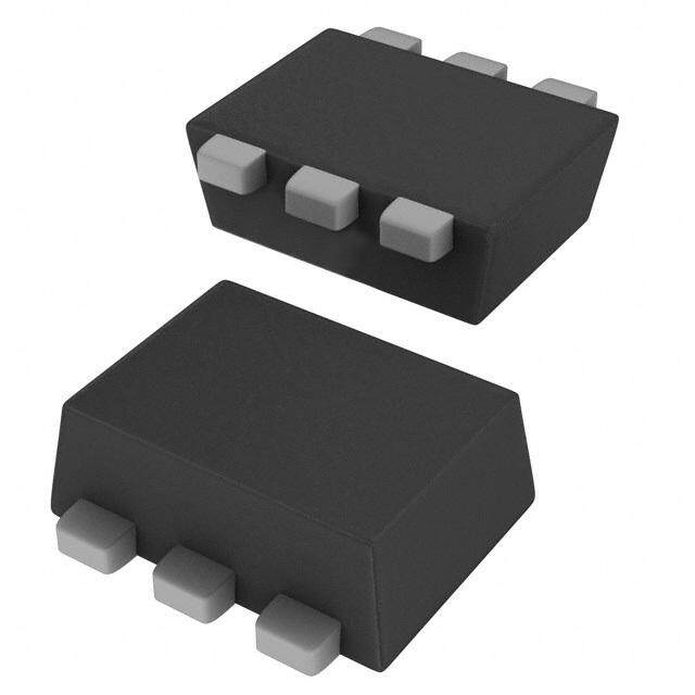
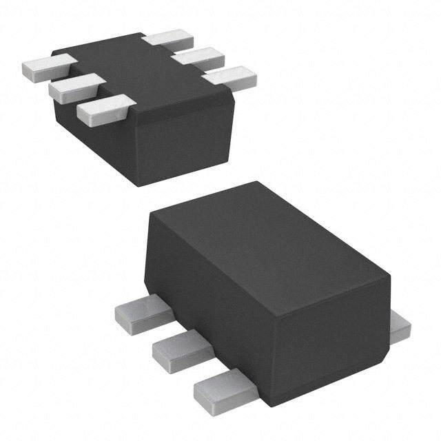
| 产品图片 |
|
| rohs | 符合RoHS无铅 / 符合限制有害物质指令(RoHS)规范要求 |
| 产品系列 | 晶体管,MOSFET,ON Semiconductor NTMD6N02R2G- |
| 数据手册 | |
| 产品型号 | NTMD6N02R2G |
| PCN设计/规格 | |
| Pd-PowerDissipation | 2 W |
| Pd-功率耗散 | 2 W |
| RdsOn-Drain-SourceResistance | 35 mOhms |
| RdsOn-漏源导通电阻 | 35 mOhms |
| Vds-Drain-SourceBreakdownVoltage | 20 V |
| Vds-漏源极击穿电压 | 20 V |
| Vgs-Gate-SourceBreakdownVoltage | +/- 12 V |
| Vgs-栅源极击穿电压 | 12 V |
| 上升时间 | 35 ns, 50 ns |
| 下降时间 | 60 ns, 80 ns |
| 不同Id时的Vgs(th)(最大值) | 1.2V @ 250µA |
| 不同Vds时的输入电容(Ciss) | 1100pF @ 16V |
| 不同Vgs时的栅极电荷(Qg) | 20nC @ 4.5V |
| 不同 Id、Vgs时的 RdsOn(最大值) | 35 毫欧 @ 6A,4.5V |
| 产品种类 | MOSFET |
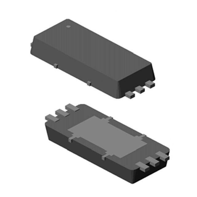
| 供应商器件封装 | 8-SOIC N |
| 其它名称 | NTMD6N02R2GOSCT |
| 典型关闭延迟时间 | 45 ns |
| 功率-最大值 | 730mW |
| 功率耗散 | 2 W |
| 包装 | 剪切带 (CT) |
| 商标 | ON Semiconductor |
| 安装类型 | 表面贴装 |
| 安装风格 | SMD/SMT |
| 导通电阻 | 35 mOhms |
| 封装 | Reel |
| 封装/外壳 | 8-SOIC(0.154",3.90mm 宽) |
| 封装/箱体 | SOIC-8 Narrow |
| 工厂包装数量 | 2500 |
| 晶体管极性 | N-Channel |
| 最大工作温度 | + 150 C |
| 最小工作温度 | - 55 C |
| 标准包装 | 1 |
| 正向跨导-最小值 | 10 S |
| 汲极/源极击穿电压 | 20 V |
| 漏极连续电流 | 5.07 A |
| 漏源极电压(Vdss) | 20V |
| 电流-连续漏极(Id)(25°C时) | 3.92A |
| 系列 | NTMD6N02 |
| 通道模式 | Enhancement |
| 配置 | Dual Dual Drain |
| 闸/源击穿电压 | +/- 12 V |


- 商务部:美国ITC正式对集成电路等产品启动337调查
- 曝三星4nm工艺存在良率问题 高通将骁龙8 Gen1或转产台积电
- 太阳诱电将投资9.5亿元在常州建新厂生产MLCC 预计2023年完工
- 英特尔发布欧洲新工厂建设计划 深化IDM 2.0 战略
- 台积电先进制程称霸业界 有大客户加持明年业绩稳了
- 达到5530亿美元!SIA预计今年全球半导体销售额将创下新高
- 英特尔拟将自动驾驶子公司Mobileye上市 估值或超500亿美元
- 三星加码芯片和SET,合并消费电子和移动部门,撤换高东真等 CEO
- 三星电子宣布重大人事变动 还合并消费电子和移动部门
- 海关总署:前11个月进口集成电路产品价值2.52万亿元 增长14.8%


PDF Datasheet 数据手册内容提取
NTMD6N02R2 MOSFET – Power, Dual, N-Channel Enhancement Mode, SO-8 6.0 A, 20 V http://onsemi.com Features • Ultra Low R VDSS RDS(ON) TYP ID MAX DS(on) • Higher Efficiency Extending Battery Life 20 V 35 m(cid:2) @ VGS = 4.5 V 6.0 A • Logic Level Gate Drive • Miniature Dual SOIC−8 Surface Mount Package • N−Channel Diode Exhibits High Speed, Soft Recovery D • Avalanche Energy Specified • SOIC−8 Mounting Information Provided • Pb−Free Package is Available G Applications • DC−DC Converters S • Low Voltage Motor Control • Power Management in Portable and Battery−Powered Products, SOIC−8 for example, Computers, Printers, Cellular and Cordless Telephones 8 CASE 751 and PCMCIA Cards 1 STYLE 11 MAXIMUM RATINGS (TJ = 25°C unless otherwise noted) Rating Symbol Value Unit MARKING DIAGRAM Drain−to−Source Voltage VDSS 20 V & PIN ASSIGNMENT Drain−to−Gate Voltage (RGS = 1.0 M(cid:2)) VDGR 20 V 1 8 Gate−to−Source Voltage − Continuous VGS (cid:2)12 V Source 1 Drain 1 2 AE 7 Thermal Resistance, Gate 1 L6 Drain 1 TJoutnacl tPioonw−etor −DAismsbipieantiot n(N @ot eT A1 )= 25°C RP(cid:3)DJA 622.0.5 °CW/W Source 2 34 (cid:2)YW(cid:2)N02 65 Drain 2 Continuous Drain Current @ TA = 25°C ID 6.5 A Gate 2 Drain 2 Continuous Drain Current @ TA = 70°C ID 5.5 A (Top View) Pulsed Drain Current (Note 4) IDM 50 A Thermal Resistance, E6N02 = Specific Device Code Junction−to−Ambient (Note 2) R(cid:3)JA 102 °C/W A = Assembly Location Total Power Dissipation @ TA = 25°C PD 1.22 W Y = Year Continuous Drain Current @ TA = 25°C ID 5.07 A WW = Work Week Continuous Drain Current @ TA = 70°C ID 4.07 A (cid:2) = Pb−Free Package Pulsed Drain Current (Note 4) IDM 40 A (Note: Microdot may be in either location) Thermal Resistance Junction−to−Ambient (Note 3) R(cid:3)JA 172 °C/W ORDERING INFORMATION Total Power Dissipation @ TA = 25°C PD 0.73 W Continuous Drain Current @ TA = 25°C ID 3.92 A Device Package Shipping† Continuous Drain Current @ TA = 70°C ID 3.14 A NTMD6N02R2 SOIC−8 2500/Tape & Reel Pulsed Drain Current (Note 4) IDM 30 A 1. Mounted onto a 2 in square FR−4 Board NTMD6N02R2G SOIC−8 2500/Tape & Reel (1 in sq. 2 oz. Cu 0.06 in thick single sided), t < 10 seconds. (Pb−Free) 2. Mounted onto a 2 in square FR−4 Board †For information on tape and reel specifications, (1 in sq. 2 oz. Cu 0.06 in thick single sided), t = steady state. including part orientation and tape sizes, please 3. Minimum FR−4 or G−10 PCB, t = steady state. 4. Pulse Test: Pulse Width = 10 (cid:4)s, Duty Cycle = 2%. refer to our Tape and Reel Packaging Specification Brochure, BRD8011/D. © Semiconductor Components Industries, LLC, 2005 1 Publication Order Number: May, 2019 − Rev. 3 NTMD6N02R2/D
NTMD6N02R2 MAXIMUM RATINGS (TJ = 25°C unless otherwise noted) (continued) Rating Symbol Value Unit Operating and Storage Temperature Range TJ, Tstg −55 to +150 °C Single Pulse Drain−to−Source Avalanche Energy − Starting TJ = 25°C EAS 360 mJ (VDD = 20 Vdc, VGS = 5.0 Vdc, Peak IL = 6.0 Apk, L = 20 mH, RG = 25 (cid:2)) Maximum Lead Temperature for Soldering Purposes for 10 seconds TL 260 °C ELECTRICAL CHARACTERISTICS (TC = 25°C unless otherwise noted) (Note 5) Characteristic Symbol Min Typ Max Unit OFF CHARACTERISTICS Drain−to−Source Breakdown Voltage V(BR)DSS Vdc (VGS = 0 Vdc, ID = 250 (cid:4)Adc) 20 − − Temperature Coefficient (Positive) − 19.2 − mV/°C Zero Gate Voltage Drain Current IDSS (cid:4)Adc (VDS = 20 Vdc, VGS = 0 Vdc, TJ = 25°C) − − 1.0 (VDS = 20 Vdc, VGS = 0 Vdc, TJ = 125°C) − − 10 Gate−Body Leakage Current (VGS = +12 Vdc, VDS = 0 Vdc) IGSS − − 100 nAdc Gate−Body Leakage Current (VGS = −12 Vdc, VDS = 0 Vdc) IGSS − − −100 nAdc ON CHARACTERISTICS Gate Threshold Voltage VGS(th) Vdc (VDS = VGS, ID = −250 (cid:4)Adc) 0.6 0.9 1.2 Temperature Coefficient (Negative) − −3.0 − mV/°C Static Drain−to−Source On−State Resistance RDS(on) (cid:2) (VGS = 4.5 Vdc, ID = 6.0 Adc) − 0.028 0.035 (VGS = 4.5 Vdc, ID = 4.0 Adc) − 0.028 0.043 (VGS = 2.7 Vdc, ID = 2.0 Adc) − 0.033 0.048 (VGS = 2.5 Vdc, ID = 3.0 Adc) − 0.035 0.049 Forward Transconductance (VDS = 12 Vdc, ID = 3.0 Adc) gFS − 10 − Mhos DYNAMIC CHARACTERISTICS Input Capacitance Ciss − 785 1100 pF Output Capacitance (VDS = 1f6 = V 1d.c0, MVHGSz) = 0 Vdc, Coss − 260 450 Reverse Transfer Capacitance Crss − 75 180 SWITCHING CHARACTERISTICS (Notes 6 and 7) Turn−On Delay Time td(on) − 12 20 ns Rise Time (VDD = 16 Vdc, ID = 6.0 Adc, tr − 50 90 VGS = 4.5 Vdc, Turn−Off Delay Time RG = 6.0 (cid:2)) td(off) − 45 75 Fall Time tf − 80 130 Turn−On Delay Time td(on) − 11 18 ns Rise Time (VDD = 16 Vdc, ID = 4.0 Adc, tr − 35 65 VGS = 4.5 Vdc, Turn−Off Delay Time RG = 6.0 (cid:2)) td(off) − 45 75 Fall Time tf − 60 110 Total Gate Charge (VDS = 16 Vdc, Qtot − 12 20 nC Gate−Source Charge VGS = 4.5 Vdc, Qgs − 1.5 − Gate−Drain Charge ID = 6.0 Adc) Qgd − 4.0 − 5. Handling precautions to protect against electrostatic discharge is mandatory 6. Indicates Pulse Test: Pulse Width =300 (cid:4)s max, Duty Cycle = 2%. 7. Switching characteristics are independent of operating junction temperature. http://onsemi.com 2
NTMD6N02R2 ELECTRICAL CHARACTERISTICS (TC = 25°C unless otherwise noted) (continued) (Note 8) Characteristic Symbol Min Typ Max Unit BODY−DRAIN DIODE RATINGS (Note 9) Diode Forward On−Voltage (IS = 4.0 Adc, VGS = 0 Vdc) VSD − 0.83 1.1 Vdc (IS = 6.0 Adc, VGS = 0 Vdc) − 0.88 1.2 (IS = 6.0 Adc, VGS = 0 Vdc, TJ = 125°C) − 0.75 − Reverse Recovery Time trr − 30 − ns (IS = d6I.S0/ dAt d=c ,1 V00G SA /=(cid:4) s0) Vdc, ta − 15 − tb − 15 − Reverse Recovery Stored Charge QRR − 0.02 − (cid:4)C 8. Handling precautions to protect against electrostatic discharge is mandatory. 9. Indicates Pulse Test: Pulse Width =300 (cid:4)s max, Duty Cycle = 2%. 12 12 MPS) 10 10 V 2.5 V 4.5 V 2.0T VJ = 25°C MPS) 10 VDS ≥ 10 V RENT (A 8 3.2 V 1.8 V RENT (A 8 R 6 R 6 U U C C N N 25°C RAI 4 RAI 4 100°C D D I, D 2 VGS = 1.5 V I, D 2 TJ = −55°C 0 0 0 0.25 0.5 0.75 1 1.25 1.5 1.75 0.5 1 1.5 2 2.5 VDS, DRAIN−TO−SOURCE VOLTAGE (VOLTS) VGS, GATE−TO−SOURCE VOLTAGE (VOLTS) Figure 1. On−Region Characteristics Figure 2. Transfer Characteristics S) S) M M H H O O E ( 0.07 E ( 0.05 C C TAN 0.06 ITDJ == 62.50° CA TAN TJ = 25°C S S SI 0.05 SI 0.04 RE RE VGS = 2.5 V CE 0.04 CE UR UR 0.03 4.5 V O 0.03 O S S − − O O T 0.02 T − − 0.02 N N RAI 0.01 RAI D D , on) 00 2 4 6 8 10 , on)0.011 3 5 7 9 11 13 DS( VGS, GATE−TO−SOURCE VOLTAGE (VOLTS) DS( ID, DRAIN CURRENT (AMPS) R R Figure 3. On−Resistance versus Figure 4. On-Resistance versus Drain Current Gate−To−Source Voltage and Gate Voltage http://onsemi.com 3
NTMD6N02R2 E 1.6 1000 NC VGS = 0 V A SIST 1.4 IVDG =S 6=. 04 .A5 V A) 100 TJ = 125°C E n E R E ( 100°C RCD)1.2 AG 10 UE K O−SOMALIZ 1 , LEAS 1 25°C TR S AIN−(NO0.8 ID 0.1 R D , on) 0.6 0.01 S( −50 −25 0 25 50 75 100 125 150 4 8 12 16 20 D R TJ, JUNCTION TEMPERATURE (°C) VDS, DRAIN−TO−SOURCE VOLTAGE (VOLTS) Figure 5. On−Resistance Variation with Figure 6. Drain−To−Source Leakage Current Temperature versus Voltage 2500 S)5 20S) VDS = 0 V VGS = 0 V TJ = 25°C OLT QT OLT V V pF)2000 Ciss GE (4 VDS 16GE ( E ( TA VGS TA CITANC1500 Crss CE VOL3 ID = 6 A 12CE VOL PA1000 UR2 Q1 Q2 VDS = 16 V 8 UR C, CA Ciss O−SO VTJG =S =2 54°.C5 V O−SO 500 T1 4 T Crss Coss ATE− AIN− 0 G 0 0 R 10 5 0 5 10 15 20 , GS 0 4 8 12 16 , DS VGS VDS V Qg, TOTAL GATE CHARGE (nC) VD GATE−TO−SOURCE OR DRAIN−TO−SOURCE VOLTAGE (VOLTS) Figure 7. Capacitance Variation Figure 8. Gate−To−Source and Drain−To−Source Voltage versus Total Charge 1000 VDS = 16 V ID = 6.0 A VGS = 4.5 V s) n E ( 100 M TI tf t, tr td(off) td(on) 10 1 10 100 RG, GATE RESISTANCE (OHMS) Figure 9. Resistive Switching Time Variation versus Gate Resistance http://onsemi.com 4
NTMD6N02R2 DRAIN−TO−SOURCE DIODE CHARACTERISTICS 5 100 VGS = 20 V RENT (AMPS) 34 VTJG =S =2 50° CV RENT (AMPS) 10 STCIN =G 2L5E° CPULSE 110 m0 s(cid:4)s R R U U C C 10 ms CE 2 N R AI 1 U R O D , SS 1 I, D RTHDSE(RonM) ALILM LITIMIT I PACKAGE LIMIT dc 0 0.1 0 0.2 0.4 0.6 0.8 1.0 1.2 0.1 1 10 100 VSD, SOURCE−TO−DRAIN VOLTAGE (VOLTS) VDS, DRAIN−TO−SOURCE VOLTAGE (VOLTS) Figure 10. Diode Forward Voltage versus Current Figure 11. Maximum Rated Forward Biased Safe Operating Area di/dt IS trr ta tb TIME tp 0.25 IS IS Figure 12. Diode Reverse Recovery Waveform TYPICAL ELECTRICAL CHARACTERISTICS 1 T N D = 0.5 E SIE 0.2 NC AN 0.1 RA 0.1 TT VE SIS 0.05 ECTIL RE 0.02 P(pk) R(cid:3)JC(t) = r(t) R(cid:3)JC EFFRMA 0.01 0.01 DPU CLUSREV TERSA AINP PSLHYO FWONR POWER Rthja(t), THE SINGLE PULSE DUTtY1 CtY2CLE, D = t1/t2 RTJE(pAkD) - T TIMC E= APT(p tk1) R(cid:3)JC(t) 0.001 1.0E−05 1.0E−04 1.0E−03 1.0E−02 1.0E−01 1.0E+00 1.0E+01 1.0E+02 1.0E+03 t, TIME (s) Figure 13. Thermal Response http://onsemi.com 5
NTMD6N02R2 PACKAGE DIMENSIONS SOIC−8 CASE 751−07 ISSUE AG NOTES: −X− 1. DIMENSIONING AND TOLERANCING PER ANSI Y14.5M, 1982. A 2. CONTROLLING DIMENSION: MILLIMETER. 3. DIMENSION A AND B DO NOT INCLUDE MOLD PROTRUSION. 4. MAXIMUM MOLD PROTRUSION 0.15 (0.006) 8 5 PER SIDE. 5. DIMENSION D DOES NOT INCLUDE DAMBAR B S 0.25 (0.010) M Y M PROTRUSION. ALLOWABLE DAMBAR PROTRUSION SHALL BE 0.127 (0.005) TOTAL 1 IN EXCESS OF THE D DIMENSION AT −Y− 4 K 6. 7M5A1X−I0M1U TMH RMUA T7E51R−IA0L6 CAROEN DOIBTSIOONL.ETE. NEW STANDARD IS 751−07. G MILLIMETERS INCHES DIM MIN MAX MIN MAX C NX 45(cid:3) A 4.80 5.00 0.189 0.197 B 3.80 4.00 0.150 0.157 SEATING PLANE C 1.35 1.75 0.053 0.069 −Z− D 0.33 0.51 0.013 0.020 G 1.27 BSC 0.050 BSC 0.10 (0.004) H 0.10 0.25 0.004 0.010 H D M J J 0.19 0.25 0.007 0.010 K 0.40 1.27 0.016 0.050 M 0 (cid:3) 8 (cid:3) 0 (cid:3) 8 (cid:3) N 0.25 0.50 0.010 0.020 0.25 (0.010)M Z Y S X S S 5.80 6.20 0.228 0.244 STYLE 11: PIN 1. SOURCE 1 2. GATE 1 3. SOURCE 2 4. GATE 2 5. DRAIN 2 6. DRAIN 2 SOLDERING FOOTPRINT* 7. DRAIN 1 8. DRAIN 1 1.52 0.060 7.0 4.0 0.275 0.155 SCALE 6:1 0.6 1.270 (cid:3) (cid:4) 0.024 0.050 mm inches *For additional information on our Pb−Free strategy and soldering details, please download the ON Semiconductor Soldering and Mounting Techniques Reference Manual, SOLDERRM/D. ON Semiconductor and are registered trademarks of Semiconductor Components Industries, LLC (SCILLC). SCILLC reserves the right to make changes without further notice to any products herein. SCILLC makes no warranty, representation or guarantee regarding the suitability of its products for any particular purpose, nor does SCILLC assume any liability arising out of the application or use of any product or circuit, and specifically disclaims any and all liability, including without limitation special, consequential or incidental damages. “Typical” parameters which may be provided in SCILLC data sheets and/or specifications can and do vary in different applications and actual performance may vary over time. All operating parameters, including “Typicals” must be validated for each customer application by customer’s technical experts. SCILLC does not convey any license under its patent rights nor the rights of others. SCILLC products are not designed, intended, or authorized for use as components in systems intended for surgical implant into the body, or other applications intended to support or sustain life, or for any other application in which the failure of the SCILLC product could create a situation where personal injury or death may occur. Should Buyer purchase or use SCILLC products for any such unintended or unauthorized application, Buyer shall indemnify and hold SCILLC and its officers, employees, subsidiaries, affiliates, and distributors harmless against all claims, costs, damages, and expenses, and reasonable attorney fees arising out of, directly or indirectly, any claim of personal injury or death associated with such unintended or unauthorized use, even if such claim alleges that SCILLC was negligent regarding the design or manufacture of the part. SCILLC is an Equal Opportunity/Affirmative Action Employer. This literature is subject to all applicable copyright laws and is not for resale in any manner. PUBLICATION ORDERING INFORMATION LITERATURE FULFILLMENT: N. American Technical Support: 800−282−9855 Toll Free ON Semiconductor Website: http://onsemi.com Literature Distribution Center for ON Semiconductor USA/Canada P.O. Box 61312, Phoenix, Arizona 85082−1312 USA Order Literature: http://www.onsemi.com/litorder Phone: 480−829−7710 or 800−344−3860 Toll Free USA/Canada Japan: ON Semiconductor, Japan Customer Focus Center Fax: 480−829−7709 or 800−344−3867 Toll Free USA/Canada 2−9−1 Kamimeguro, Meguro−ku, Tokyo, Japan 153−0051 For additional information, please contact your Email: orderlit@onsemi.com Phone: 81−3−5773−3850 local Sales Representative. http://onsemi.com NTMD6N02R2/D 6
Mouser Electronics Authorized Distributor Click to View Pricing, Inventory, Delivery & Lifecycle Information: O N Semiconductor: NTMD6N02R2G