ICGOO在线商城 > 分立半导体产品 > 晶体管 - FET,MOSFET - 单 > MTB50P03HDLT4G

 Datasheet下载
- 型号: MTB50P03HDLT4G
- 制造商: ON Semiconductor
- 库位|库存: xxxx|xxxx
- 要求:
| 数量阶梯 | 香港交货 | 国内含税 |
| +xxxx | $xxxx | ¥xxxx |
查看当月历史价格
查看今年历史价格
MTB50P03HDLT4G产品简介:
ICGOO电子元器件商城为您提供MTB50P03HDLT4G由ON Semiconductor设计生产,在icgoo商城现货销售,并且可以通过原厂、代理商等渠道进行代购。 MTB50P03HDLT4G价格参考。ON SemiconductorMTB50P03HDLT4G封装/规格:晶体管 - FET,MOSFET - 单, 表面贴装 P 沟道 30V 50A(Tc) 2.5W(Ta),125W(Tc) D2PAK。您可以下载MTB50P03HDLT4G参考资料、Datasheet数据手册功能说明书,资料中有MTB50P03HDLT4G 详细功能的应用电路图电压和使用方法及教程。
MTB50P03HDLT4G 是安森美半导体(ON Semiconductor)生产的一款P沟道增强型MOSFET,主要应用于需要高效功率控制的场景。该器件具有低导通电阻、高耐压和大电流承载能力,适用于以下应用场景:

1. 电源管理:用于DC-DC转换器、电源开关和负载管理,实现高效的能量转换与分配。
2. 电机控制:在直流电机驱动电路中作为功率开关,提供快速响应和稳定性能。
3. 电池供电设备:如笔记本电脑、平板和工业设备,用于电池充放电管理和电源路径控制。
4. 汽车电子:用于车载电源系统、电动工具及辅助电机控制,具备良好的热稳定性和可靠性。
5. 工业自动化:作为高频率开关元件,用于PLC、继电器驱动及传感器供电控制。

其封装形式(如DPAK或TO-252)便于散热和安装,适合高密度电路设计。
| 参数 | 数值 |
| 产品目录 | |
| ChannelMode | Enhancement |
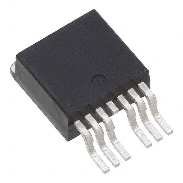
| 描述 | MOSFET P-CH 30V 50A D2PAKMOSFET PFET D2PAK 30V 50A 25mOhm |
| 产品分类 | FET - 单分离式半导体 |
| FET功能 | 逻辑电平门 |
| FET类型 | MOSFET P 通道,金属氧化物 |
| Id-ContinuousDrainCurrent | 50 A |
| Id-连续漏极电流 | 50 A |
| 品牌 | ON Semiconductor |
| 产品手册 | |
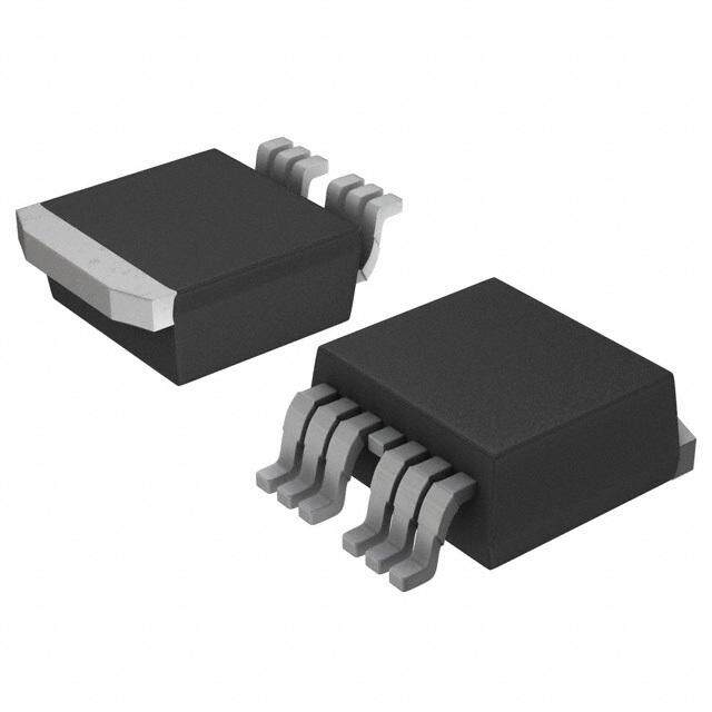
| 产品图片 |
|
| rohs | 符合RoHS无铅 / 符合限制有害物质指令(RoHS)规范要求 |
| 产品系列 | 晶体管,MOSFET,ON Semiconductor MTB50P03HDLT4G- |
| 数据手册 | |
| 产品型号 | MTB50P03HDLT4G |
| Pd-PowerDissipation | 125 W |
| Pd-功率耗散 | 125 W |
| RdsOn-Drain-SourceResistance | 25 mOhms |
| RdsOn-漏源导通电阻 | 25 mOhms |
| Vds-Drain-SourceBreakdownVoltage | - 30 V |
| Vds-漏源极击穿电压 | - 30 V |
| Vgs-Gate-SourceBreakdownVoltage | +/- 15 V |
| Vgs-栅源极击穿电压 | 15 V |
| 上升时间 | 340 ns |
| 下降时间 | 218 ns |
| 不同Id时的Vgs(th)(最大值) | 2V @ 250µA |
| 不同Vds时的输入电容(Ciss) | 4900pF @ 25V |
| 不同Vgs时的栅极电荷(Qg) | 100nC @ 5V |
| 不同 Id、Vgs时的 RdsOn(最大值) | 25 毫欧 @ 25A,5V |
| 产品目录页面 | |
| 产品种类 | MOSFET |
| 供应商器件封装 | D2PAK |
| 其它名称 | MTB50P03HDLT4GOSDKR |
| 典型关闭延迟时间 | 90 ns |
| 功率-最大值 | 2.5W |
| 包装 | Digi-Reel® |
| 商标 | ON Semiconductor |
| 安装类型 | 表面贴装 |
| 安装风格 | SMD/SMT |
| 封装 | Reel |
| 封装/外壳 | TO-263-3,D²Pak(2 引线+接片),TO-263AB |
| 封装/箱体 | D2PAK-2 |
| 工厂包装数量 | 800 |
| 晶体管极性 | P-Channel |
| 最大工作温度 | + 150 C |
| 最小工作温度 | - 55 C |
| 标准包装 | 1 |
| 正向跨导-最小值 | 20 S |
| 漏源极电压(Vdss) | 30V |
| 电流-连续漏极(Id)(25°C时) | 50A (Tc) |
| 系列 | MTB50P03HDL |
| 通道模式 | Enhancement |
| 配置 | Single |


PDF Datasheet 数据手册内容提取
MTB50P03HDL Preferred Device Power MOSFET 50 Amps, 30 Volts, Logic Level P−Channel D2PAK This Power MOSFET is designed to withstand high energy in the avalanche and commutation modes. The energy efficient design also offers a drain−to−source diode with a fast recovery time. Designed for http://onsemi.com low voltage, high speed switching applications in power supplies, converters and PWM motor controls, these devices are particularly 50 AMPERES well suited for bridge circuits where diode speed and commutating 30 VOLTS safe operating areas are critical and offer additional safety margin R = 25 m(cid:2) against unexpected voltage transients. DS(on) Features P−Channel • Avalanche Energy Specified D • Source−to−Drain Diode Recovery Time Comparable to a Discrete Fast Recovery Diode • Diode is Characterized for Use in Bridge Circuits • G I and V Specified at Elevated Temperature DSS DS(on) • Short Heatsink Tab Manufactured − Not Sheared • S Specially Designed Leadframe for Maximum Power Dissipation • Pb−Free Packages are Available 4 MAXIMUM RATINGS (TC = 25°C unless otherwise noted) D2PAK CASE 418B Rating Symbol Value Unit 1 2 STYLE 2 Drain−Source Voltage VDSS 30 Vdc 3 Drain−Gate Voltage (RGS = 1.0 M(cid:2)) VDGR 30 Vdc MARKING DIAGRAM Gate−Source Voltage − Continuous VGS ±15 Vdc & PIN ASSIGNMENT − Non−Repetitive (tp ≤ 10 ms) VGSM ±20 Vpk 4 Drain Current − Continuous ID 50 Adc Drain Drain Current − Continuous @ 100°C ID 31 Drain Current − Single Pulse (tp ≤ 10 (cid:3)s) IDM 150 Apk Total Power Dissipation PD 125 W M TB Derate above 25°C 1.0 W/°C 50P03HG Total Power Dissipation @ TC = 25°C, when 2.5 W AYWW mounted with the minimum recommended pad size Operating and Storage Temperature Range TJ, Tstg −55 to °C 150 2 Drain Single Pulse Drain−to−Source Avalanche EAS 1250 mJ 1 3 Energy − Starting TJ = 25°C Gate Source (VDD = 25 Vdc, VGS = 5.0 Vdc, Peak IL = 50 Apk, L = 1.0 mH, RG = 25 (cid:2)) MTB50P03H = Device Code Thermal Resistance °C/W A = Assembly Location − Junction−to−Case R(cid:4)JC 1.0 Y = Year − Junction−to−Ambient R(cid:4)JA 62.5 WW = Work Week − Junction−to−Ambient, when mounted with the R(cid:4)JA 50 G = Pb−Free Package minimum recommended pad size Maximum Lead Temperature for Soldering TL 260 °C ORDERING INFORMATION Purposes, 1/8″ from case for 10 seconds See detailed ordering and shipping information in the package Stresses exceeding Maximum Ratings may damage the device. Maximum dimensions section on page 7 of this data sheet. Ratings are stress ratings only. Functional operation above the Recommended Operating Conditions is not implied. Extended exposure to stresses above the Preferred devices are recommended choices for future use Recommended Operating Conditions may affect device reliability. and best overall value. © Semiconductor Components Industries, LLC, 2006 1 Publication Order Number: June, 2006 − Rev. 6 MTB50P03HDL/D
MTB50P03HDL ELECTRICAL CHARACTERISTICS (TJ = 25°C unless otherwise noted) Characteristic Symbol Min Typ Max Unit OFF CHARACTERISTICS Drain−to−Source Breakdown Voltage (Cpk ≥ 2.0) (Note 3) V(BR)DSS Vdc (VGS = 0 Vdc, ID = 250 (cid:3)Adc) 30 − − Temperature Coefficient (Positive) − 26 − mV/°C Zero Gate Voltage Drain Current IDSS (cid:3)Adc (VDS = 30 Vdc, VGS = 0 Vdc) − − 1.0 (VDS = 30 Vdc, VGS = 0 Vdc, TJ = 125°C) − − 10 Gate−Body Leakage Current IGSS nAdc (VGS = ±15 Vdc, VDS = 0 Vdc) − − 100 ON CHARACTERISTICS (Note 1) Gate Threshold Voltage (Cpk ≥ 3.0) (Note 3) VGS(th) Vdc (VDS = VGS, ID = 250 (cid:3)Adc) 1.0 1.5 2.0 Threshold Temperature Coefficient (Negative) − 4.0 − mV/°C Static Drain−Source On−Resistance (Cpk ≥ 3.0) (Note 3) RDS(on) m(cid:2) (VGS = 5.0 Vdc, ID = 25 Adc) − 20.9 25 Drain−Source On−Voltage (VGS = 5.0 Vdc) VDS(on) Vdc (ID = 50 Adc) − 0.83 1.5 (ID = 25 Adc, TJ =125°C) − − 1.3 Forward Transconductance gFS mhos (VDS = 5.0 Vdc, ID = 25 Adc) 15 20 − DYNAMIC CHARACTERISTICS Input Capacitance Ciss − 3500 4900 pF Output Capacitance (VDS = 25 Vdc, VGS = 0 Vdc, f = 1.0 MHz) Coss − 1550 2170 Transfer Capacitance Crss − 550 770 SWITCHING CHARACTERISTICS (Note 2) Turn−On Delay Time td(on) − 22 30 ns Rise Time (VDD= 15 Vdc, ID = 50 Adc, tr − 340 466 Turn−Off Delay Time VGS = 5.0 Vdc, RG = 2.3 (cid:2)) td(off) − 90 117 Fall Time tf − 218 300 Gate Charge (See Figure 8) QT − 74 100 nC (VDS = 24 Vdc, ID = 50 Adc, Q1 − 13.6 − VGS = 5.0 Vdc) Q2 − 44.8 − Q3 − 35 − SOURCE−DRAIN DIODE CHARACTERISTICS Forward On−Voltage (IS = 5(0IS A =d c5,0 V AGdSc =, V0G VSd =c ,0 T VJ d=c 1)25°C) VSD −− 21..3894 3−.0 Vdc Reverse Recovery Time trr − 106 − ns (See Figure 15) (IS = 50 Adc, VGS = 0 Vdc, ta − 58 − dIS/dt = 100 A/(cid:3)s) tb − 48 − Reverse Recovery Stored Charge QRR − 0.246 − (cid:3)C INTERNAL PACKAGE INDUCTANCE Internal Drain Inductance LD − 3.5 − nH (Measured from the drain lead 0.25″ from package to center of die) Internal Source Inductance LS − 7.5 − nH (Measured from the source lead 0.25″ from package to source bond pad) 1. Pulse Test: Pulse Width ≤300 (cid:3)s, Duty Cycle ≤ 2%. 2. Switching characteristics are independent of operating junction temperature. 3. Reflects typical values. Max limit − Typ Cpk = 3 x SIGMA http://onsemi.com 2
MTB50P03HDL TYPICAL ELECTRICAL CHARACTERISTICS 100 100 TJ = 25°C VGS = 10 V 5 V VDS ≥ 5 V TJ = −(cid:2)55°C MPS) 80 68 V V MPS) 80 25°C 100°C NT (A 4.5 V 4 V NT (A RE 60 RE 60 R R U U RAIN C 40 3.5 V RAIN C 40 D D , D 3 V , D I 20 I 20 2.5 V 0 0 0 0.2 0.4 0.6 0.8 1.0 1.2 1.4 1.6 1.8 2.0 1.5 1.9 2.3 2.7 3.1 3.5 3.9 4.3 VDS, DRAIN−TO−SOURCE VOLTAGE (VOLTS) VGS, GATE−TO−SOURCE VOLTAGE (VOLTS) Figure 1. On−Region Characteristics Figure 2. Transfer Characteristics S) S) M M H 0.029 H 0.022 E (O VGS = 5 V E (O TJ = 25°C VGS = 5 V C 0.027 C 0.021 N N A A T T S S RESI 0.025 TJ = 100°C RESI 0.020 CE 0.023 CE 0.019 R R U 25°C U O O S 0.021 S 0.018 − − O O T T N− 0.019 N− 0.017 AI AI R R 10 V , Dn)0.017 −(cid:2)55°C , Dn)0.016 o o DS(0.015 DS(0.015 R 0 20 40 60 80 100 R 0 20 40 60 80 100 ID, DRAIN CURRENT (AMPS) ID, DRAIN CURRENT (AMPS) Figure 3. On−Resistance versus Drain Current Figure 4. On−Resistance versus Drain Current and Temperature and Gate Voltage E 1.35 1000 C AN VGS = 5 V VGS = 0 V SIST 1.25 ID = 25 A E R CE D) nA) TJ = 125°C URZE1.15 E ( −SOMALI KAG 100 AIN−TO(NOR1.05 , LEASS R D , Dn) 0.95 I S(o 100°C D R 0.85 10 −(cid:2)50 −(cid:2)25 0 25 50 75 100 125 150 0 5 10 15 20 25 30 TJ, JUNCTION TEMPERATURE (°C) VDS, DRAIN−TO−SOURCE VOLTAGE (VOLTS) Figure 5. On−Resistance Variation with Figure 6. Drain−to−Source Leakage Temperature Current versus Voltage http://onsemi.com 3
MTB50P03HDL POWER MOSFET SWITCHING Switching behavior is most easily modeled and predicted The capacitance (C ) is read from the capacitance curve at iss by recognizing that the power MOSFET is charge a voltage corresponding to the off−state condition when controlled. The lengths of various switching intervals ((cid:5)t) calculating t and is read at a voltage corresponding to the d(on) are determined by how fast the FET input capacitance can on−state when calculating t . d(off) be charged by current from the generator. At high switching speeds, parasitic circuit elements complicate the analysis. The inductance of the MOSFET The published capacitance data is difficult to use for source lead, inside the package and in the circuit wiring which calculating rise and fall because drain−gate capacitance varies greatly with applied voltage. Accordingly, gate is common to both the drain and gate current paths, produces a voltage at the source which reduces the gate drive current. charge data is used. In most cases, a satisfactory estimate of The voltage is determined by Ldi/dt, but since di/dt is a average input current (I ) can be made from a G(AV) rudimentary analysis of the drive circuit so that function of drain current, the mathematical solution is complex. The MOSFET output capacitance also complicates t = Q/I G(AV) the mathematics. And finally, MOSFETs have finite internal During the rise and fall time interval when switching a gate resistance which effectively adds to the resistance of the resistive load, V remains virtually constant at a level driving source, but the internal resistance is difficult to GS known as the plateau voltage, V . Therefore, rise and fall measure and, consequently, is not specified. SGP times may be approximated by the following: The resistive switching time variation versus gate resistance (Figure 9) shows how typical switching t = Q x R /(V − V ) r 2 G GG GSP performance is affected by the parasitic circuit elements. If t = Q x R /V f 2 G GSP the parasitics were not present, the slope of the curves would where maintain a value of unity regardless of the switching speed. The circuit used to obtain the data is constructed to minimize V = the gate drive voltage, which varies from zero to V GG GG common inductance in the drain and gate circuit loops and R = the gate drive resistance G is believed readily achievable with board mounted and Q2 and VGSP are read from the gate charge curve. components. Most power electronic loads are inductive; the data in the figure is taken with a resistive load, which During the turn−on and turn−off delay times, gate current is approximates an optimally snubbed inductive load. Power not constant. The simplest calculation uses appropriate MOSFETs may be safely operated into an inductive load; values from the capacitance curves in a standard equation for however, snubbing reduces switching losses. voltage change in an RC network. The equations are: td(on) = RG Ciss In [VGG/(VGG − VGSP)] t = R C In (V /V ) d(off) G iss GG GSP 14000 12000 CVisDsS = 0 V VGS = 0 V TJ = 25°C F) 10000 p E ( C N 8000 A CIT Crss A 6000 P A C, C 4000 Ciss Coss 2000 Crss 0 10 5 0 5 10 15 20 25 VGS VDS GATE−TO−SOURCE OR DRAIN−TO−SOURCE VOLTAGE (VOLTS) Figure 7. Capacitance Variation http://onsemi.com 4
MTB50P03HDL GE (VOLTS) 65 QT VGS 3205GE (VOLTS) 1000 VVDGDS == 3100 VV ITDJ == 5205 °AC tr VOLTA 4 Q1 Q2 20VOLTA tf ATE−TO−SOURCE 32 ITDJ == 5205 °AC 1150RAIN−TO−SOURCE t, TIME (ns) 100 ttdd((oonff)) V, GGS 1 Q3 VDS 5 V, DDS 0 0 10 0 10 20 30 40 50 60 70 80 1 10 QT, TOTAL GATE CHARGE (nC) RG, GATE RESISTANCE (Ohms) Figure 8. Gate−To−Source and Drain−To−Source Figure 9. Resistive Switching Time Voltage versus Total Charge Variation versus Gate Resistance DRAIN−TO−SOURCE DIODE CHARACTERISTICS The switching characteristics of a MOSFET body diode high di/dts. The diode’s negative di/dt during t is directly a are very important in systems using it as a freewheeling or controlled by the device clearing the stored charge. commutating diode. Of particular interest are the reverse However, the positive di/dt during t is an uncontrollable b recovery characteristics which play a major role in diode characteristic and is usually the culprit that induces determining switching losses, radiated noise, EMI and RFI. current ringing. Therefore, when comparing diodes, the System switching losses are largely due to the nature of ratio of t /t serves as a good indicator of recovery b a the body diode itself. The body diode is a minority carrier abruptness and thus gives a comparative estimate of device, therefore it has a finite reverse recovery time, t , due probable noise generated. A ratio of 1 is considered ideal and rr to the storage of minority carrier charge, Q , as shown in values less than 0.5 are considered snappy. RR the typical reverse recovery wave form of Figure 12. It is this Compared to ON Semiconductor standard cell density stored charge that, when cleared from the diode, passes low voltage MOSFETs, high cell density MOSFET diodes through a potential and defines an energy loss. Obviously, are faster (shorter t ), have less stored charge and a softer rr repeatedly forcing the diode through reverse recovery reverse recovery characteristic. The softness advantage of further increases switching losses. Therefore, one would the high cell density diode means they can be forced through like a diode with short t and low Q specifications to reverse recovery at a higher di/dt than a standard cell rr RR minimize these losses. MOSFET diode without increasing the current ringing or the The abruptness of diode reverse recovery effects the noise generated. In addition, power dissipation incurred amount of radiated noise, voltage spikes, and current from switching the diode will be less due to the shorter ringing. The mechanisms at work are finite irremovable recovery time and lower switching losses. circuit parasitic inductances and capacitances acted upon by 50 VGS = 0 V S) TJ = 25°C MP 40 A T ( N E R 30 R U C E C R 20 U O S , S I 10 0 0.4 0.6 0.8 1.0 1.2 1.4 1.6 1.8 2.0 2.2 2.4 VSD, SOURCE−TO−DRAIN VOLTAGE (VOLTS) Figure 10. Diode Forward Voltage versus Current http://onsemi.com 5
MTB50P03HDL di/dt = 300 A/(cid:3)s Standard Cell Density trr T High Cell Density N RE trr CUR ta tb E C R U O S , S I t, TIME Figure 11. Reverse Recovery Time (t ) rr SAFE OPERATING AREA The Forward Biased Safe Operating Area curves define reliable operation, the stored energy from circuit inductance the maximum simultaneous drain−to−source voltage and dissipated in the transistor while in avalanche must be less drain current that a transistor can handle safely when it is than the rated limit and must be adjusted for operating forward biased. Curves are based upon maximum peak conditions differing from those specified. Although industry junction temperature and a case temperature (T ) of 25°C. practice is to rate in terms of energy, avalanche energy C Peak repetitive pulsed power limits are determined by using capability is not a constant. The energy rating decreases the thermal response data in conjunction with the procedures non−linearly with an increase of peak current in avalanche discussed in AN569, “Transient Thermal Resistance − and peak junction temperature. General Data and Its Use.” Although many E−FETs can withstand the stress of Switching between the off−state and the on−state may drain−to−source avalanche at currents up to rated pulsed traverse any load line provided neither rated peak current current (I ), the energy rating is specified at rated DM (I ) nor rated voltage (V ) is exceeded, and that the continuous current (I ), in accordance with industry DM DSS D transition time (t, t) does not exceed 10 (cid:3)s. In addition the custom. The energy rating must be derated for temperature r f total power averaged over a complete switching cycle must as shown in the accompanying graph (Figure 13). Maximum not exceed (TJ(MAX) − TC)/(R(cid:4)JC). energy at currents below rated continuous ID can safely be A power MOSFET designated E−FET can be safely used assumed to equal the values indicated. in switching circuits with unclamped inductive loads. For 1000 1400 E VGS = 20 V RC ID = 50 A SINGLE PULSE U 1200 S) TC = 25°C −SOmJ) MP TOY (1000 T (A 100 100 (cid:3)s AIN−ERG EN DREN 800 N CURR 1 ms PULSE ANCHE 600 I, DRAID 10 RTHDSE(RonM) ALILM LITIMIT 10d mcs , SINGLE SAVAL 420000 A PACKAGE LIMIT E 1 0 0.1 1.0 10 100 25 50 75 100 125 150 VDS, DRAIN−TO−SOURCE VOLTAGE (VOLTS) TJ, STARTING JUNCTION TEMPERATURE (°C) Figure 12. Maximum Rated Forward Biased Figure 13. Maximum Avalanche Energy versus Safe Operating Area Starting Junction Temperature http://onsemi.com 6
MTB50P03HDL TYPICAL ELECTRICAL CHARACTERISTICS E C AN 1.0 T SIS D = 0.5 E R L A M 0.2 R NT THEALIZED) 0.1 0.1 P(pk) SIERM 0.05 R(cid:4)JC(t) = r(t) R(cid:4)JC NO D CURVES APPLY FOR POWER RA(N 0.02 PULSE TRAIN SHOWN T VE 0.01 t1 READ TIME AT t1 CTI t2 TJ(pk) − TC = P(pk) R(cid:4)JC(t) FE SINGLE PULSE DUTY CYCLE, D = t1/t2 F E 0.01 r(t), 1.0E−05 1.0E−04 1.0E−03 1.0E−02 1.0E−01 1.0E+00 1.0E+01 t, TIME (s) Figure 14. Thermal Response 3 R(cid:4)JA = 50°C/W Board material = 0.065 mil FR−4 2.5 Mounted on the minimum recommended footprint TS) Collector/Drain Pad Size ≈450 mils x 350 mils T A W 2.0 N ( di/dt O TI IS PA 1.5 SI S trr R DI 1 ta tb E W TIME O P 0.5 , D tp 0.25 IS P 0 IS 25 50 75 100 125 150 TA, AMBIENT TEMPERATURE (°C) Figure 15. Diode Reverse Recovery Waveform Figure 16. D2PAK Power Derating Curve ORDERING INFORMATION Device Package Shipping† MTB50P03HDL D2PAK MTB50P03HDLG D2PAK 50 Units / Rail (Pb−Free) MTB50P03HDLT4 D2PAK MTB50P03HDLT4G D2PAK 800 / Tape & Reel (Pb−Free) †For information on tape and reel specifications, including part orientation and tape sizes, please refer to our Tape and Reel Packaging Specifications Brochure, BRD8011/D. http://onsemi.com 7
MTB50P03HDL PACKAGE DIMENSIONS D2PAK 3 CASE 418B−04 ISSUE J C NOTES: 1. DIMENSIONING AND TOLERANCING PER ANSI Y14.5M, 1982. E 2. CONTROLLING DIMENSION: INCH. −B− V 3. 418B−01 THRU 418B−03 OBSOLETE, W NEW STANDARD 418B−04. 4 INCHES MILLIMETERS DIM MIN MAX MIN MAX A 0.340 0.380 8.64 9.65 A B 0.380 0.405 9.65 10.29 C 0.160 0.190 4.06 4.83 S 1 2 3 D 0.020 0.035 0.51 0.89 E 0.045 0.055 1.14 1.40 F 0.310 0.350 7.87 8.89 G 0.100 BSC 2.54 BSC −T− K H 0.080 0.110 2.03 2.79 SEATING W J 0.018 0.025 0.46 0.64 PLANE G J K 0.090 0.110 2.29 2.79 L 0.052 0.072 1.32 1.83 H M 0.280 0.320 7.11 8.13 D3 PL N 0.197 REF 5.00 REF P 0.079 REF 2.00 REF 0.13 (0.005)M T B M R 0.039 REF 0.99 REF S 0.575 0.625 14.60 15.88 VARIABLE V 0.045 0.055 1.14 1.40 CONFIGURATION ZONE N P STYLE 2: PIN 1.GATE R U 2.DRAIN 3.SOURCE L L L 4.DRAIN M M M F F F VIEW W−W VIEW W−W VIEW W−W 1 2 3 SOLDERING FOOTPRINT* 8.38 0.33 10.66 1.016 5.08 0.42 0.04 0.20 3.05 0.12 17.02 0.67 (cid:2) (cid:3) mm SCALE 3:1 inches *For additional information on our Pb−Free strategy and soldering details, please download the ON Semiconductor Soldering and Mounting Techniques Reference Manual, SOLDERRM/D. http://onsemi.com 8
MTB50P03HDL ON Semiconductor and are registered trademarks of Semiconductor Components Industries, LLC (SCILLC). SCILLC reserves the right to make changes without further notice to any products herein. SCILLC makes no warranty, representation or guarantee regarding the suitability of its products for any particular purpose, nor does SCILLC assume any liability arising out of the application or use of any product or circuit, and specifically disclaims any and all liability, including without limitation special, consequential or incidental damages. “Typical” parameters which may be provided in SCILLC data sheets and/or specifications can and do vary in different applications and actual performance may vary over time. All operating parameters, including “Typicals” must be validated for each customer application by customer’s technical experts. SCILLC does not convey any license under its patent rights nor the rights of others. SCILLC products are not designed, intended, or authorized for use as components in systems intended for surgical implant into the body, or other applications intended to support or sustain life, or for any other application in which the failure of the SCILLC product could create a situation where personal injury or death may occur. Should Buyer purchase or use SCILLC products for any such unintended or unauthorized application, Buyer shall indemnify and hold SCILLC and its officers, employees, subsidiaries, affiliates, and distributors harmless against all claims, costs, damages, and expenses, and reasonable attorney fees arising out of, directly or indirectly, any claim of personal injury or death associated with such unintended or unauthorized use, even if such claim alleges that SCILLC was negligent regarding the design or manufacture of the part. SCILLC is an Equal Opportunity/Affirmative Action Employer. This literature is subject to all applicable copyright laws and is not for resale in any manner. PUBLICATION ORDERING INFORMATION LITERATURE FULFILLMENT: N. American Technical Support: 800−282−9855 Toll Free ON Semiconductor Website: www.onsemi.com Literature Distribution Center for ON Semiconductor USA/Canada P.O. Box 5163, Denver, Colorado 80217 USA Europe, Middle East and Africa Technical Support: Order Literature: http://www.onsemi.com/orderlit Phone: 303−675−2175 or 800−344−3860 Toll Free USA/Canada Phone: 421 33 790 2910 Fax: 303−675−2176 or 800−344−3867 Toll Free USA/Canada Japan Customer Focus Center For additional information, please contact your local Email: orderlit@onsemi.com Phone: 81−3−5773−3850 Sales Representative http://onsemi.com MTB50P03HDL/D 9
Mouser Electronics Authorized Distributor Click to View Pricing, Inventory, Delivery & Lifecycle Information: O N Semiconductor: MTB50P03HDLT4G