ICGOO在线商城 > 分立半导体产品 > 晶体管 - FET,MOSFET - 单 > FDMS86202
 Datasheet下载
- 型号: FDMS86202
- 制造商: Fairchild Semiconductor
- 库位|库存: xxxx|xxxx
- 要求:
| 数量阶梯 | 香港交货 | 国内含税 |
| +xxxx | $xxxx | ¥xxxx |
查看当月历史价格
查看今年历史价格
FDMS86202产品简介:
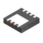
ICGOO电子元器件商城为您提供FDMS86202由Fairchild Semiconductor设计生产,在icgoo商城现货销售,并且可以通过原厂、代理商等渠道进行代购。 FDMS86202价格参考。Fairchild SemiconductorFDMS86202封装/规格:晶体管 - FET,MOSFET - 单, 表面贴装 N 沟道 120V 13.5A(Ta) 2.7W(Ta),156W(Tc) Power56。您可以下载FDMS86202参考资料、Datasheet数据手册功能说明书,资料中有FDMS86202 详细功能的应用电路图电压和使用方法及教程。
ON Semiconductor的FDMS86202是一款高性能、低导通电阻(Rds(on))的N沟道MOSFET,广泛应用于多种电力电子设备中。该器件具有出色的开关性能和较低的功耗,适用于以下应用场景:

1. 电源管理:
   - FDMS86202常用于直流-直流转换器(DC-DC Converter),如降压(Buck)、升压(Boost)和升降压(Buck-Boost)转换器。其低导通电阻有助于减少传导损耗,提高转换效率。
   - 在开关电源(SMPS)中,它作为主开关管或同步整流管,能够有效降低开关损耗和导通损耗。

2. 电机驱动:
   - 该MOSFET适合用于无刷直流电机(BLDC)和步进电机的驱动电路。其快速开关特性和低导通电阻可以减少发热,提高电机控制的精度和效率。
   - 在电动工具、家电(如洗衣机、空调等)中,FDMS86202可用于驱动电机,确保高效运行。

3. 电池管理系统(BMS):
   - 在锂电池保护电路中,FDMS86202可以用作充放电路径的开关,实现过流、短路和过温保护。其低导通电阻减少了电池内部损耗,延长了电池寿命。

4. 负载开关:
   - 作为负载开关,FDMS86202可以用于便携式电子设备(如智能手机、平板电脑等)中,实现快速响应的电源切换,同时减少静态电流消耗。

5. 汽车电子:
   - 在汽车电子系统中,如车载充电器、LED照明驱动、电动助力转向(EPS)等,FDMS86202凭借其高可靠性和耐高温特性,能够在严苛的工作环境下稳定工作。

总之,FDMS86202凭借其卓越的电气性能和可靠性,成为众多电力电子应用中的理想选择,特别是在需要高效能、低损耗和高可靠性的场合。
| 参数 | 数值 |
| 产品目录 | |
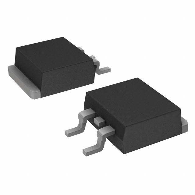
| 描述 | MOSFET N-CH 120V 8MLPMOSFET CCI MOSFET |
| 产品分类 | FET - 单分离式半导体 |
| FET功能 | 标准 |
| FET类型 | MOSFET N 通道,金属氧化物 |
| Id-ContinuousDrainCurrent | 40 A |
| Id-连续漏极电流 | 40 A |
| 品牌 | Fairchild Semiconductor |
| 产品手册 | |
| 产品图片 |
|
| 产品系列 | 晶体管,MOSFET,Fairchild Semiconductor FDMS86202PowerTrench® |
| 数据手册 | |
| 产品型号 | FDMS86202 |
| PCN组件/产地 | |
| Pd-PowerDissipation | 156 W |
| Pd-功率耗散 | 156 W |
| Qg-GateCharge | 45 nC |
| Qg-栅极电荷 | 45 nC |
| RdsOn-Drain-SourceResistance | 10.9 mOhms |
| RdsOn-漏源导通电阻 | 10.9 mOhms |
| rohs | 无铅 / 符合限制有害物质指令(RoHS)规范要求 |
| Vds-Drain-SourceBreakdownVoltage | 120 V |
| Vds-漏源极击穿电压 | 120 V |
| Vgs-Gate-SourceBreakdownVoltage | 20 V |
| Vgs-栅源极击穿电压 | 20 V |
| Vgsth-Gate-SourceThresholdVoltage | 3.1 V |
| Vgsth-栅源极阈值电压 | 3.1 V |
| 上升时间 | 6 ns |
| 下降时间 | 5 ns |
| 不同Id时的Vgs(th)(最大值) | 4V @ 250µA |
| 不同Vds时的输入电容(Ciss) | 4250pF @ 60V |
| 不同Vgs时的栅极电荷(Qg) | 64nC @ 10V |
| 不同 Id、Vgs时的 RdsOn(最大值) | 7.2 毫欧 @ 13.5A, 10V |
| 产品种类 | MOSFET |
| 供应商器件封装 | Power56 |
| 其它名称 | FDMS86202CT |
| 典型关闭延迟时间 | 27 ns |
| 功率-最大值 | 2.7W |
| 包装 | 剪切带 (CT) |
| 单位重量 | 4.376 g |
| 商标 | Fairchild Semiconductor |
| 安装类型 | 表面贴装 |
| 安装风格 | SMD/SMT |
| 封装 | Reel |
| 封装/外壳 | 8-PowerTDFN |
| 封装/箱体 | Power-56-8 |
| 工厂包装数量 | 3000 |
| 晶体管极性 | N-Channel |
| 最大工作温度 | + 150 C |
| 最小工作温度 | - 55 C |
| 标准包装 | 1 |
| 正向跨导-最小值 | 44 S |
| 漏源极电压(Vdss) | 120V |
| 特色产品 | http://www.digikey.cn/product-highlights/cn/zh/fairchild-cloud-systems-computing/4301 |
| 电流-连续漏极(Id)(25°C时) | 13.5A (Ta) |
| 系列 | FDMS86202 |
| 配置 | Single Quad Drain |


PDF Datasheet 数据手册内容提取
Is Now Part of To learn more about ON Semiconductor, please visit our website at www.onsemi.com Please note: As part of the Fairchild Semiconductor integration, some of the Fairchild orderable part numbers will need to change in order to meet ON Semiconductor’s system requirements. Since the ON Semiconductor product management systems do not have the ability to manage part nomenclature that utilizes an underscore (_), the underscore (_) in the Fairchild part numbers will be changed to a dash (-). This document may contain device numbers with an underscore (_). Please check the ON Semiconductor website to verify the updated device numbers. The most current and up-to-date ordering information can be found at www.onsemi.com. Please email any questions regarding the system integration to Fairchild_questions@onsemi.com. ON Semiconductor and the ON Semiconductor logo are trademarks of Semiconductor Components Industries, LLC dba ON Semiconductor or its subsidiaries in the United States and/or other countries. ON Semiconductor owns the rights to a number of patents, trademarks, copyrights, trade secrets, and other intellectual property. A listing of ON Semiconductor’s product/patent coverage may be accessed at www.onsemi.com/site/pdf/Patent-Marking.pdf. ON Semiconductor reserves the right to make changes without further notice to any products herein. ON Semiconductor makes no warranty, representation or guarantee regarding the suitability of its products for any particular purpose, nor does ON Semiconductor assume any liability arising out of the application or use of any product or circuit, and specifically disclaims any and all liability, including without limitation special, consequential or incidental damages. Buyer is responsible for its products and applications using ON Semiconductor products, including compliance with all laws, regulations and safety requirements or standards, regardless of any support or applications information provided by ON Semiconductor. “Typical” parameters which may be provided in ON Semiconductor data sheets and/or specifications can and do vary in different applications and actual performance may vary over time. All operating parameters, including “Typicals” must be validated for each customer application by customer’s technical experts. ON Semiconductor does not convey any license under its patent rights nor the rights of others. ON Semiconductor products are not designed, intended, or authorized for use as a critical component in life support systems or any FDA Class 3 medical devices or medical devices with a same or similar classification in a foreign jurisdiction or any devices intended for implantation in the human body. Should Buyer purchase or use ON Semiconductor products for any such unintended or unauthorized application, Buyer shall indemnify and hold ON Semiconductor and its officers, employees, subsidiaries, affiliates, and distributors harmless against all claims, costs, damages, and expenses, and reasonable attorney fees arising out of, directly or indirectly, any claim of personal injury or death associated with such unintended or unauthorized use, even if such claim alleges that ON Semiconductor was negligent regarding the design or manufacture of the part. ON Semiconductor is an Equal Opportunity/Affirmative Action Employer. This literature is subject to all applicable copyright laws and is not for resale in any manner.
F D M S 8 July 2014 6 2 FDMS86202 0 2 ® N N-Channel Shielded Gate PowerTrench MOSFET - C 120 V, 64 A, 7.2 mΩ h a Features General Description n n e (cid:132) Shielded Gate MOSFET Technology This N-Channel MOSFET is produced using Fairchild l Semiconductor’s advanced PowerTrench® process that S (cid:132) Max rDS(on) = 7.2 mΩ at VGS = 10 V, ID = 13.5 A incorporates Shielded Gate technology. This process has been hi optimized for the on-state resistance and yet maintain superior e (cid:132) Max rDS(on) = 10.3 mΩ at VGS = 6 V, ID = 11.5 A switching performance. ld e (cid:132) Advanced Package and Silicon combination for low r DS(on) d and high efficiency Application G (cid:132) MSL1 robust package design a (cid:132) DC-DC Conversion t e (cid:132) 100% UIL tested P o (cid:132) RoHS Compliant w e r T r e n c Top Bottom h Pin 1 ® S S D Pin 1 S M S O G S D S F S D E D T D D D G D Power 56 MOSFET Maximum Ratings TA = 25 °C unless otherwise noted Symbol Parameter Ratings Units V Drain to Source Voltage 120 V DS V Gate to Source Voltage ±20 V GS Drain Current -Continuous T = 25 °C 64 C I -Continuous T = 25 °C (Note 1a) 13.5 A D A -Pulsed (Note 4) 240 E Single Pulse Avalanche Energy (Note 3) 600 mJ AS Power Dissipation T = 25 °C 156 P C W D Power Dissipation T = 25 °C (Note 1a) 2.7 A T , T Operating and Storage Junction Temperature Range -55 to +150 °C J STG Thermal Characteristics R Thermal Resistance, Junction to Case 0.8 θJC °C/W R Thermal Resistance, Junction to Ambient (Note 1a) 45 θJA Package Marking and Ordering Information Device Marking Device Package Reel Size Tape Width Quantity FDMS86202 FDMS86202 Power 56 13 ’’ 12 mm 3000 units ©2013 Fairchild Semiconductor Corporation 1 www.fairchildsemi.com FDMS86202 Rev. C3
F Electrical Characteristics T = 25 °C unless otherwise noted D J M Symbol Parameter Test Conditions Min Typ Max Units S 8 Off Characteristics 6 2 BV Drain to Source Breakdown Voltage I = 250 μA, V = 0 V 120 V 0 DSS D GS 2 ΔBVDSS Breakdown Voltage Temperature I = 250 μA, referenced to 25 °C 103 mV/°C N ΔTJ Coefficient D -C IDSS Zero Gate Voltage Drain Current VDS = 96 V, VGS = 0 V 1 μA h a I Gate to Source Leakage Current V = ±20 V, V = 0 V ±100 nA GSS GS DS n n On Characteristics e l V Gate to Source Threshold Voltage V = V , I = 250 μA 2.0 3.1 4.0 V S GS(th) GS DS D h ΔVGS(th) Gate to Source Threshold Voltage I = 250 μA, referenced to 25 °C -10 mV/°C ie ΔTJ Temperature Coefficient D ld V = 10 V, I = 13.5 A 6.0 7.2 e GS D d rDS(on) Static Drain to Source On Resistance VGS = 6 V, ID = 11.5 A 8.1 10.3 mΩ G VGS = 10 V, ID = 13.5 A,TJ = 125 °C 10.9 13.2 a t gFS Forward Transconductance VDS = 5 V, ID = 13.5 A 44 S e P Dynamic Characteristics o w Ciss Input Capacitance 3195 4250 pF e Coss Output Capacitance Vf =D S1 =M 6H0z V, VGS = 0 V, 449 600 pF rT r Crss Reverse Transfer Capacitance 17 30 pF e n Rg Gate Resistance 0.1 0.9 2.7 Ω c h Switching Characteristics ® M t Turn-On Delay Time 21 33 ns d(on) O tr Rise Time VDD = 60 V, ID = 13.5 A, 6 13 ns S td(off) Turn-Off Delay Time VGS = 10 V, RGEN = 6 Ω 27 44 ns FE tf Fall Time 5 11 ns T Q Total Gate Charge V = 0 V to 10 V 45 64 nC g GS Qg Total Gate Charge VGS = 0 V to 6 V VDD = 60 V, 29 41 nC Qgs Gate to Source Charge ID = 13.5 A 14.3 nC Q Gate to Drain “Miller” Charge 8.7 nC gd Drain-Source Diode Characteristics V = 0 V, I = 2.1 A (Note 2) 0.69 1.2 V Source to Drain Diode Forward Voltage GS S V SD V = 0 V, I = 13.5 A (Note 2) 0.76 1.3 GS S t Reverse Recovery Time 73 118 ns rr I = 13.5 A, di/dt = 100 A/μs Q Reverse Recovery Charge F 117 187 nC rr Notes: 1. RθJA is determined with the device mounted on a 1in2 pad 2 oz copper pad on a 1.5 x 1.5 in. board of FR-4 material. RθJC is guaranteed by design while RθCA is determined by the user's board design. a)45 °C/W when mounted on a b)115 °C/W when mounted on a 1 in2 pad of 2 oz copper minimum pad of 2 oz copper. GDDSS GDDSS FSFS FSFS 2. Pulse Test: Pulse Width < 300 μs, Duty cycle < 2.0%. 3. EAS of 600 mJ is based on starting TJ = 25 °C, L = 3 mH, IAS = 20 A, VDD = 120 V, VGS = 10 V. 100% test at L = 0.1 mH, IAS = 65 A. 4. Pulse Id limited by junction temperature, td ≤ 100 μs, please refer to SOA curve for more details. ©2013 Fairchild Semiconductor Corporation 2 www.fairchildsemi.com FDMS86202 Rev. C3
F D Typical Characteristics M T = 25 °C unless otherwise noted J S 8 6 2 240 5 0 VGS = 10 V PULSE DURATION = 80 μs CE V = 5 V 2 A)180 VGS = 8 V DUTY CYCLE = 0.5% MAX STAN 4 GS N-C T ( VGS = 7 V ESI VGS = 6 V h DRAIN CURREN16200 VGS = 6 V NORMALIZEDO SOURCE ON-R 23 VGS = 8 V VGS = 7 V annel Shi I, D VGS = 5 V AIN T 1 PULSE DURATION = 80 μs VGS = 10 V eld R DUTY CYCLE = 0.5% MAX e 0 D 0 d 0 1 2 3 4 5 0 60 120 180 240 G VDS, DRAIN TO SO URCE VOLTAGE (V) ID, DRAIN CURR ENT (A) a t e Figure 1. On Region Characteristics Figure 2. Normalized On-Resistance P vs Drain Current and Gate Voltage o w e r T 2.4 40 r e STANCE 22..02 VIDG =S 1=3 1.50 AV ()E mΩ 30 PDUULTSYE C DYUCRLEA T=I O0.N5 %= 8M0A μXs nch® NORMALIZED O SOURCE ON-RESI 11111.....02468 rDRAIN TO ,DS(on)RCE ON-RESISTANC 1200 ID = 1T3J. =5 1A25 oC MOSFET N T 0.8 OU RAI 0.6 S TJ = 25 oC D 0.4 0 -75 -50 -25 0 25 50 75 100 125 150 4 5 6 7 8 9 10 TJ, JUNCTION TEM PERATURE (oC) VGS, GATE TO SOURCE VOLTAGE (V) Figure 3. Normalized On Resistance Figure 4. On-Resistance vs Gate to vs Junction Temperature Source Voltage 240 300 PDUULTSYE C DYUCRLEA T=I O0.N5 %= 8M0A μXs T (A) 100 VGS = 0 V N A)180 RE 10 T ( VDS = 10 V UR URREN120 RAIN C 1 TJ = 150 oC RAIN C TJ = 150 oC TJ = 25 oC ERSE D 0.1 TJ = 25 oC D 60 V I, D TJ = -55 oC I, RES 0.01 TJ = -55 oC 0 0.001 2 3 4 5 6 7 8 0.0 0.2 0.4 0.6 0.8 1.0 1.2 VGS, GATE TO SOU RCE VOLTAGE (V) VSD, BODY DIODE FOR WARD VOLTAGE (V) Figure 5. Transfer Characteristics Figure 6. Source to Drain Diode Forward Voltage vs Source Current ©2013 Fairchild Semiconductor Corporation 3 www.fairchildsemi.com FDMS86202 Rev. C3
F D Typical Characteristics M T = 25 °C unless otherwise noted J S 8 6 2 10 10000 0 TAGE (V) 8 ID = 13.5 A VDD = 35 V 1000 Ciss 2 N-C OL VDD = 60 V pF) h O SOURCE V 46 VDD = 85 V PACITANCE ( 100 Coss annel S ATE T 2 CA 10 Crss hie G f = 1 MHz l , GS VGS = 0 V de V 0 1 d 0 10 20 30 40 50 0.1 1 10 100 G Qg, GATE CH ARGE (nC) VDS, DRAIN TO SOU RCE VOLTAGE (V) a t e Figure 7. Gate Charge Characteristics Figure 8. Capacitance vs Drain P to Source Voltage o w e r 100 T 100 r e n A) A) 80 c NT ( NT ( h® E E ANCHE CURR 10 TJ = 25 oTCJ = 100 oC DRAIN CURR 4600 Limited by Package VGS = 6 VVGS = 10 V MOSFE AVAL TJ = 125 oC , ID 20 T I, AS RθJC = 0.8 oC/W 1 0 25 50 75 100 125 150 0.01 0.1 1 10 100 1000 tAV, TIME IN AVA LANCHE (ms) TC, CASE TEMPERATURE (oC) Figure 9. Unclamped Inductive Figure 10. Maximum Continuous Drain Switching Capability Current vs Case Temperature 1000 50000 W) SINGLE PULSE T (A) 100 10 us OWER (10000 TRCθJ =C 2=5 0 o.C8 oC/W REN T P CUR 10 THIS AREA IS SIEN AIN LIMITED BY rDS(on) 100 us RAN1000 R SINGLE PULSE T I, DD 1 RTTJCθ J ==C M2=5A 0 Xo.C8 R oCA/TWED CMUERAVSEU RBEEDN TD ATTOA 11D0 mC mss , PEAK )PK 0.1 P( 100 0.1 1 10 100 400 10-5 10-4 10-3 10-2 10-1 1 VDS, DRAIN to SOU RCE VOLTAGE (V) t, PULSE WI DTH (sec) Figure 11. Forward Bias Safe Figure 12. Single Pulse Maximum Operating Area Power Dissipation ©2013 Fairchild Semiconductor Corporation 4 www.fairchildsemi.com FDMS86202 Rev. C3
F D Typical Characteristics M T = 25 °C unless otherwise noted J S 8 6 2 2 0 T 2 EN 1 DUTY CYCLE-DESCENDING ORDER N SI AN D = 0.5 -C D EFFECTIVE TRAL RESISTANCE 0.1 00000.....21000521 PDM t1t2 hannel S EM NOTES: h MALIZTHER 0.01 SINGLE PULSE ZRθθJJCC( t=) =0 .r8( to)C x/ WRθJC ield NOR DPeuatyk CTyJ c=l eP, DDM =x tZ1 θ/J tC2(t) + TC ed r(t), 0.001 G 10-5 10-4 10-3 10-2 10-1 1 a t e t, RECTANGULAR PULSE DURATION (sec) P o w Figure 13. Junction-to-Case Transient Thermal Response Curve e r T r e n c h ® M O S F E T ©2013 Fairchild Semiconductor Corporation 5 www.fairchildsemi.com FDMS86202 Rev. C3
5.10 A 4.90 4.42 PKG 3.81 CL B 8 5 8 7 6 5 1.14 KEEP OUT AREA 3.65 PKG CL 6.25 5.90 4.79 6.61 1.27 PIN #1 1 4 IDICATOR TOP VIEW 1 2 3 4 1.27 0.61 SEE DETAIL A 3.81 5.10 LAND PATTERN SIDE VIEW RECOMMENDATION 3.81 0.10 C A B 1.27 0.47 (0.38) (8X) 0.37 1 4 (0.35) 0.65 0.55 NOTES: UNLESS OTHERWISE SPECIFIED A) PACKAGE STANDARD REFERENCE: JEDEC MO-240, ISSUE A, VAR. AA, PIN #1 B) ALL DIMENSIONS ARE IN MILLIMETERS. INDICATOR 4.66 4.46 C) DIMENSIONS DO NOT INCLUDE BURRS OR MOLD FLASH. MOLD FLASH OR BURRS DOES NOT EXCEED 0.10MM. D) DIMENSIONING AND TOLERANCING PER 8 5 ASME Y14.5M-2009. 0.70 E) IT IS RECOMMENDED TO HAVE NO TRACES 4.33 4.13 OR VIAS WITHIN THE KEEP OUT AREA. F) DRAWING FILE NAME: PQFN08JREV3. BOTTOM VIEW 0.10 C 1.10 0.90 0.08 C C 0.25 0.05 0.15 0.00 SEATING PLANE SCALE: 2:1
ON Semiconductor and are trademarks of Semiconductor Components Industries, LLC dba ON Semiconductor or its subsidiaries in the United States and/or other countries. ON Semiconductor owns the rights to a number of patents, trademarks, copyrights, trade secrets, and other intellectual property. A listing of ON Semiconductor’s product/patent coverage may be accessed at www.onsemi.com/site/pdf/Patent−Marking.pdf. ON Semiconductor reserves the right to make changes without further notice to any products herein. ON Semiconductor makes no warranty, representation or guarantee regarding the suitability of its products for any particular purpose, nor does ON Semiconductor assume any liability arising out of the application or use of any product or circuit, and specifically disclaims any and all liability, including without limitation special, consequential or incidental damages. Buyer is responsible for its products and applications using ON Semiconductor products, including compliance with all laws, regulations and safety requirements or standards, regardless of any support or applications information provided by ON Semiconductor. “Typical” parameters which may be provided in ON Semiconductor data sheets and/or specifications can and do vary in different applications and actual performance may vary over time. All operating parameters, including “Typicals” must be validated for each customer application by customer’s technical experts. ON Semiconductor does not convey any license under its patent rights nor the rights of others. ON Semiconductor products are not designed, intended, or authorized for use as a critical component in life support systems or any FDA Class 3 medical devices or medical devices with a same or similar classification in a foreign jurisdiction or any devices intended for implantation in the human body. Should Buyer purchase or use ON Semiconductor products for any such unintended or unauthorized application, Buyer shall indemnify and hold ON Semiconductor and its officers, employees, subsidiaries, affiliates, and distributors harmless against all claims, costs, damages, and expenses, and reasonable attorney fees arising out of, directly or indirectly, any claim of personal injury or death associated with such unintended or unauthorized use, even if such claim alleges that ON Semiconductor was negligent regarding the design or manufacture of the part. ON Semiconductor is an Equal Opportunity/Affirmative Action Employer. This literature is subject to all applicable copyright laws and is not for resale in any manner. PUBLICATION ORDERING INFORMATION LITERATURE FULFILLMENT: N. American Technical Support: 800−282−9855 Toll Free ON Semiconductor Website: www.onsemi.com Literature Distribution Center for ON Semiconductor USA/Canada 19521 E. 32nd Pkwy, Aurora, Colorado 80011 USA Europe, Middle East and Africa Technical Support: Order Literature: http://www.onsemi.com/orderlit Phone: 303−675−2175 or 800−344−3860 Toll Free USA/Canada Phone: 421 33 790 2910 Fax: 303−675−2176 or 800−344−3867 Toll Free USA/Canada Japan Customer Focus Center For additional information, please contact your local Email: orderlit@onsemi.com Phone: 81−3−5817−1050 Sales Representative © Semiconductor Components Industries, LLC www.onsemi.com www.onsemi.com 1
Mouser Electronics Authorized Distributor Click to View Pricing, Inventory, Delivery & Lifecycle Information: O N Semiconductor: FDMS86202