ICGOO在线商城 > 分立半导体产品 > 晶体管 - FET,MOSFET - 单 > FDMS2734
 Datasheet下载
- 型号: FDMS2734
- 制造商: Fairchild Semiconductor
- 库位|库存: xxxx|xxxx
- 要求:
| 数量阶梯 | 香港交货 | 国内含税 |
| +xxxx | $xxxx | ¥xxxx |
查看当月历史价格
查看今年历史价格
FDMS2734产品简介:
ICGOO电子元器件商城为您提供FDMS2734由Fairchild Semiconductor设计生产,在icgoo商城现货销售,并且可以通过原厂、代理商等渠道进行代购。 FDMS2734价格参考。Fairchild SemiconductorFDMS2734封装/规格:晶体管 - FET,MOSFET - 单, 表面贴装 N 沟道 250V 2.8A(Ta),14A(Tc) 2.5W(Ta),78W(Tc) 8-MLP (5x6), Power56。您可以下载FDMS2734参考资料、Datasheet数据手册功能说明书,资料中有FDMS2734 详细功能的应用电路图电压和使用方法及教程。
ON Semiconductor的FDMS2734是一款N沟道MOSFET(金属氧化物场效应晶体管),其应用场景广泛,特别是在需要高效、低损耗和高开关速度的电力电子设备中。以下是该型号的主要应用场景:

1. 电源管理:
   - DC-DC转换器:FDMS2734适用于各种DC-DC转换器,如降压、升压和升降压转换器。它能够高效地进行电压调节,确保稳定的输出电压,适用于便携式电子设备、通信设备和工业控制系统。
   - 开关电源(SMPS):在开关电源中,FDMS2734作为功率开关,能够快速切换状态,减少能量损失,提高电源效率。

2. 电机驱动:
   - 无刷直流电机(BLDC):FDMS2734可用于BLDC电机的驱动电路中,提供高效的电流控制,确保电机平稳运行,适用于无人机、电动工具和家用电器等领域。
   - 步进电机:在步进电机驱动电路中,FDMS2734可以实现精确的电流控制,提高电机的响应速度和定位精度。

3. 负载开关:
   - 电池管理系统(BMS):在电池管理系统中,FDMS2734可以用作负载开关,控制电池与负载之间的通断,保护电池免受过充、过放和短路等异常情况的影响。
   - USB电源管理:在USB充电器和移动电源中,FDMS2734可以作为负载开关,实现对不同设备的智能供电管理。

4. 信号切换:
   - 多路复用器/解复用器:FDMS2734可以用于模拟信号或多路数字信号的切换,适用于数据采集系统、测试仪器和通信设备。
   - 音频信号切换:在音频设备中,FDMS2734可以用于音频信号的切换,确保信号传输的可靠性和低失真。

5. 保护电路:
   - 过流保护:FDMS2734可以集成到过流保护电路中,当电流超过设定阈值时,迅速切断电路,防止损坏其他组件。
   - 短路保护:在短路情况下,FDMS2734能够快速响应并切断电流,保护电路免受损坏。

总之,FDMS2734凭借其低导通电阻、高开关速度和优异的热性能,在多种电力电子应用中表现出色,是设计高效、可靠电力系统的理想选择。
| 参数 | 数值 |
| 产品目录 | |
| ChannelMode | Enhancement |
| 描述 | MOSFET N-CH 250V 2.8A POWER56MOSFET 250V N-Ch UltraFET PowerTrenchAr MOSFET |
| 产品分类 | FET - 单分离式半导体 |
| FET功能 | 逻辑电平门 |
| FET类型 | MOSFET N 通道,金属氧化物 |
| Id-ContinuousDrainCurrent | 2.8 A |
| Id-连续漏极电流 | 2.8 A |
| 品牌 | Fairchild Semiconductor |
| 产品手册 | |
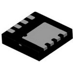
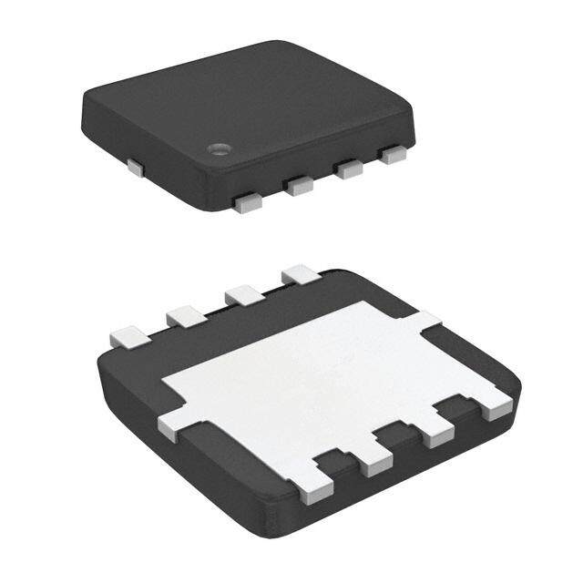
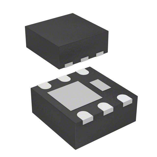
| 产品图片 |
|
| rohs | 符合RoHS无铅 / 符合限制有害物质指令(RoHS)规范要求 |
| 产品系列 | 晶体管,MOSFET,Fairchild Semiconductor FDMS2734UltraFET™ |
| 数据手册 | |
| 产品型号 | FDMS2734 |
| PCN设计/规格 | |
| Pd-PowerDissipation | 2.5 W |
| Pd-功率耗散 | 2.5 W |
| RdsOn-Drain-SourceResistance | 122 mOhms |
| RdsOn-漏源导通电阻 | 122 mOhms |
| Vds-Drain-SourceBreakdownVoltage | 250 V |
| Vds-漏源极击穿电压 | 250 V |
| Vgs-Gate-SourceBreakdownVoltage | +/- 20 V |
| Vgs-栅源极击穿电压 | 20 V |
| 上升时间 | 10 ns |
| 下降时间 | 12 ns |
| 不同Id时的Vgs(th)(最大值) | 4V @ 250µA |
| 不同Vds时的输入电容(Ciss) | 2365pF @ 100V |
| 不同Vgs时的栅极电荷(Qg) | 42nC @ 10V |
| 不同 Id、Vgs时的 RdsOn(最大值) | 122 毫欧 @ 2.8A,10V |
| 产品目录页面 | |
| 产品种类 | MOSFET |
| 供应商器件封装 | Power56 |
| 其它名称 | FDMS2734DKR |
| 典型关闭延迟时间 | 36 ns |
| 功率-最大值 | 2.5W |
| 包装 | Digi-Reel® |
| 单位重量 | 231 mg |
| 商标 | Fairchild Semiconductor |
| 安装类型 | 表面贴装 |
| 安装风格 | SMD/SMT |
| 封装 | Reel |
| 封装/外壳 | 8-MLP,Power56 |
| 封装/箱体 | MLP-8 |
| 工厂包装数量 | 3000 |
| 晶体管极性 | N-Channel |
| 最大工作温度 | + 150 C |
| 最小工作温度 | - 55 C |
| 标准包装 | 1 |
| 正向跨导-最小值 | 11 S |
| 漏源极电压(Vdss) | 250V |
| 特色产品 | http://www.digikey.cn/product-highlights/cn/zh/fairchild-cloud-systems-computing/4301 |
| 电流-连续漏极(Id)(25°C时) | 2.8A (Ta), 14A (Tc) |
| 系列 | FDMS2734 |
| 通道模式 | Enhancement |
| 配置 | Single Quad Drain Triple Source |


PDF Datasheet 数据手册内容提取
Is Now Part of To learn more about ON Semiconductor, please visit our website at www.onsemi.com Please note: As part of the Fairchild Semiconductor integration, some of the Fairchild orderable part numbers will need to change in order to meet ON Semiconductor’s system requirements. Since the ON Semiconductor product management systems do not have the ability to manage part nomenclature that utilizes an underscore (_), the underscore (_) in the Fairchild part numbers will be changed to a dash (-). This document may contain device numbers with an underscore (_). Please check the ON Semiconductor website to verify the updated device numbers. The most current and up-to-date ordering information can be found at www.onsemi.com. Please email any questions regarding the system integration to Fairchild_questions@onsemi.com. ON Semiconductor and the ON Semiconductor logo are trademarks of Semiconductor Components Industries, LLC dba ON Semiconductor or its subsidiaries in the United States and/or other countries. ON Semiconductor owns the rights to a number of patents, trademarks, copyrights, trade secrets, and other intellectual property. A listing of ON Semiconductor’s product/patent coverage may be accessed at www.onsemi.com/site/pdf/Patent-Marking.pdf. ON Semiconductor reserves the right to make changes without further notice to any products herein. ON Semiconductor makes no warranty, representation or guarantee regarding the suitability of its products for any particular purpose, nor does ON Semiconductor assume any liability arising out of the application or use of any product or circuit, and specifically disclaims any and all liability, including without limitation special, consequential or incidental damages. Buyer is responsible for its products and applications using ON Semiconductor products, including compliance with all laws, regulations and safety requirements or standards, regardless of any support or applications information provided by ON Semiconductor. “Typical” parameters which may be provided in ON Semiconductor data sheets and/or specifications can and do vary in different applications and actual performance may vary over time. All operating parameters, including “Typicals” must be validated for each customer application by customer’s technical experts. ON Semiconductor does not convey any license under its patent rights nor the rights of others. ON Semiconductor products are not designed, intended, or authorized for use as a critical component in life support systems or any FDA Class 3 medical devices or medical devices with a same or similar classification in a foreign jurisdiction or any devices intended for implantation in the human body. Should Buyer purchase or use ON Semiconductor products for any such unintended or unauthorized application, Buyer shall indemnify and hold ON Semiconductor and its officers, employees, subsidiaries, affiliates, and distributors harmless against all claims, costs, damages, and expenses, and reasonable attorney fees arising out of, directly or indirectly, any claim of personal injury or death associated with such unintended or unauthorized use, even if such claim alleges that ON Semiconductor was negligent regarding the design or manufacture of the part. ON Semiconductor is an Equal Opportunity/Affirmative Action Employer. This literature is subject to all applicable copyright laws and is not for resale in any manner.
F D M S March 2011 2 7 3 FDMS2734 4 N N-Channel UltraFET Trench® MOSFET(cid:2) -C h 250V, 14A, 122m(cid:3) a n Features General Description n e l (cid:2) Max rDS(on) = 122m(cid:3) at VGS = 10V, ID = 2.8A UItraFET devices combine characteristics that enable U l (cid:2) Max r = 130m(cid:3) at V = 6V, I = 1.7A benchmark efficiency in power conversion applications. tr DS(on) GS D Optimized for r , low ESR, low total and Miller gate charge, a (cid:2) Low Miller Charge these devices aDrSe( oidn)eal for high frequency DC to DC converters. FE (cid:2) Optimized efficiency at high frequencies Application T T (cid:2) RoHS Compliant r (cid:2) DC - DC Conversion e n c h ® M O S F E T Pin 1 S S S G D 5 4 G D 6 3 S D 7 2 S D D D D D 8 1 S Power 56 (Bottom view) MOSFET Maximum Ratings TA = 25°C unless otherwise noted Symbol Parameter Ratings Units V Drain to Source Voltage 250 V DS V Gate to Source Voltage ±20 V GS Drain Current -Continuous (Silicon limited) T = 25°C 14 C I -Continuous T = 25°C (Note 1a) 2.8 A D A -Pulsed 30 Power Dissipation T = 25°C 78 P C W D Power Dissipation T = 25°C (Note 1a) 2.5 A T , T Operating and Storage Junction Temperature Range -55 to +150 °C J STG Thermal Characteristics R(cid:4)JC Thermal Resistance, Junction to Case 1.6 °C/W R(cid:4)JA Thermal Resistance, Junction to Ambient (Note 1a) 50 Package Marking and Ordering Information Device Marking Device Package Reel Size Tape Width Quantity FDMS2734 FDMS2734 Power 56 13’’ 12mm 3000 units ©2011 Fairchild Semiconductor Corporation 1 www.fairchildsemi.com FDMS2734 Rev.C1
F D Electrical Characteristics M T = 25°C unless otherwise noted J S Symbol Parameter Test Conditions Min Typ Max Units 2 7 3 Off Characteristics 4 BV Drain to Source Breakdown Voltage I = 250(cid:5)A, V = 0V 250 V N DSS D GS - (cid:6)BV Breakdown Voltage Temperature C (cid:2)(cid:2)(cid:2)(cid:6)TDSS Coefficient ID = 250(cid:5)A, referenced to 25°C 250 mV/°C h J a I Zero Gate Voltage Drain Current V = 200V, 1 (cid:5)A n DSS DS n IGSS Gate to Source Leakage Current VGS = ±20V, VGS = 0V ±100 nA e l U On Characteristics (Note 2) l t VGS(th) Gate to Source Threshold Voltage VGS = VDS, ID = 250(cid:5)A 2 3 4 V ra (cid:2)(cid:6)VGS(th) Gate to Source Threshold Voltage I = 250(cid:5)A, referenced to 25°C -11 mV/°C FE (cid:2)(cid:2)(cid:2)(cid:6)TJ Temperature Coefficient D T V = 10V, I = 2.8A 105 122 T GS D r r Drain to Source On Resistance V = 6V, I = 1.7A 110 130 m(cid:3) e DS(on) GS D n VGS = 10V, ID = 2.8A TJ = 125°C 217 258 c h g Forward Transconductance V = 10V, I = 2.8A 11 S FS DS D ® M Dynamic Characteristics O Ciss Input Capacitance 1775 2365 pF S C Output Capacitance VDS = 100V, VGS = 0V, 80 110 pF F oss f = 1MHz E Crss Reverse Transfer Capacitance 25 40 pF T R Gate Resistance f = 1MHz 0.9 (cid:3) g Switching Characteristics t Turn-On Delay Time 22 36 ns d(on) V = 125V, I = 2.8A t Rise Time DD D 10 20 ns r V = 10V, R = 6(cid:3) t Turn-Off Delay Time GS GEN 36 58 ns d(off) t Fall Time 12 22 ns f Qg(TOT) Total Gate Charge at 10V VGS = 0V to 10V VDD = 125V 30 42 nC Q Gate to Source Gate Charge I = 2.8A 7 nC gs D Q Gate to Drain “Miller” Charge 9 nC gd Drain-Source Diode Characteristics V Source to Drain Diode Forward Voltage V = 0V, I = 2.8A (Note 2) 0.75 1.20 V SD GS S t Reverse Recovery Time 79 119 ns rr I = 2.8A, di/dt = 100A/(cid:5)s Q Reverse Recovery Charge F 214 321 nC rr Notes: 1: R(cid:4)JA is determined with the device mounted on a 1 in2 pad 2 oz copper pad on a 1.5 x 1.5 in. board of FR-4 material. R(cid:4)JC is guaranteed by design while R(cid:4)CA is determined by the user's board design. a. 50°C/W when mounted on b. 125°C/W when mounted on a a 1 in2 pad of 2 oz copper minimum pad of 2 oz copper 2: Pulse Test: Pulse Width < 300(cid:5)s, Duty cycle < 2.0%. FDMS2734 Rev.C1 2 www.fairchildsemi.com
F D Typical Characteristics M T = 25°C unless otherwise noted J S 2 7 3 30 2.2 4 PULSE DURATION = 80(cid:5)s CE PULSE DURATION = 80(cid:5)s N URRENT (A)122505 DUTY CYCLE =V G0.S5 %= M 10AVX VVGGSS = = 6 5VV ALIZEDE ON-RESISTAN 112...680 VGS = 4.5V DUTY CYCVGLSE == 50V.5%MAX -Channe N C ORM URC 1.4 VGS = 6V l U DRAI10 VGS = 4.5V NO SO 1.2 ltra I, D 5 AIN T 1.0 VGS = 10V FE 0 DR 0.8 T 0 1 2 3 4 5 0 5 10 15 20 25 30 T r VDS, DRAIN TO SO URCE VOLTAGE (V) ID, DRAIN CUR RENT(A) en Figure 1. On Region Characteristics Figure 2. Normalized On-Resistance c vs Drain Current and Gate Voltage h ® M 2.4 400 O TANCE22..02 VIDG S= =2 .180AV )(cid:3)m ID = 7A PDUULTSYE C DYUCRLEA T=I O0.N5 %= M80A(cid:5)Xs SFE ALIZEDE ON-RESIS111...468 RAIN TO (SISTANCE 234200 TJ = 150oC T NORM N TO SOURC0011....6802 r, DDS(on) URCE ON-RE160 TJ = 25oC AI O R0.4 S 80 D -75 -50 -25 0 25 50 75 100 125 150 4 6 8 10 TJ, JUNCTION TEM PERATURE (oC) VGS, GATE TO SOUR CE VOLTAGE (V) Figure 3. Normalized On Resistance Figure 4. On-Resistance vs Gate to vs Junction Temperature Source Voltage 16 20 PULSE DURATION = 80(cid:5)s A) 10 VGS = 0V NT (A) 12 DUTY CYCLE = 0.5%MAX ENT ( RE TJ = 150oC RR 1 TJ = -55oC CUR 8 TJ = -55oC N CU TJ = 150oC N AI 0.1 , DRAID 4 TJ = 25oC RSE DR0.01 TJ = 25oC I E V E R 0 , S1E-3 I 2 3 4 5 6 0.0 0.2 0.4 0.6 0.8 1.0 1.2 VGS, GATE TO SOU RCE VOLTAGE (V) VSD, BODY DIODE FOR WARD VOLTAGE (V) Figure 5. Transfer Characteristics Figure 6. Source to Drain Diode Forward Voltage vs Source Current FDMS2734 Rev.C1 3 www.fairchildsemi.com
F D Typical Characteristics M T = 25°C unless otherwise noted J S 2 7 10 3000 3 V) 4 AGE( 8 1000 Ciss N-C T E VOL 6 VDD =75V VDD = 125V E (pF) Coss han C C n SOUR 4 VDD = 175V CITAN 100 el U ATE TO 2 CAPA f = 1MHz Crss ltraF G E , GS 0 10 VGS = 0V T V 0 8 16 24 32 0.1 1 10 100 T r Qg, GATE CH ARGE(nC) VDS, DRAIN TO SO URCE VOLTAGE (V) e n Figure 7. Gate Charge Characteristics Figure 8. Capacitance vs Drain c to Source Voltage h ® M 4 15 O S NT(A) 3 A) 12 VGS = 10V FET RE T ( ANCHE CUR 2 TJ = 125oC TJ = 25oC AIN CURREN 69 VGS = 6V L R A D 3 , AVS I, D R(cid:4)JC = 1.6oC/W A I 1 0 0.01 0.1 0.5 25 50 75 100 125 150 tAV, TIME IN AV ALANCHE(ms) TC, CASE TEMPE RATURE (oC) Figure 9. Unclamped Inductive Figure 10. Maximum Continuous Drain Switching Capability Current vs Case Temperature 40 3000 10 W)1000 FOR TEMPERATURES AIN CURRENT (A) 0.11 TLIHMISIT AERDE BAY I SrD S(on) 111 00m0 m smss ANSIENT POWER ( 10100 VGS = 10V ACUBI =RO RVI2EE5 N2T5 oAC1--S- -5-D- -F0-1-E--O2-–-R-5-L-T-A--L-A-T-OT--EAW P=SE 2:A5KoC I, DRD00.0.0011 RSTTJAI(cid:4)N J ==AG M2=L5 AE1 Xo 2PC 5RU oALCST/WEED D110 Cs s , PEAK TR)K 1 SINGLE PULSE 0.1 1 10 100 1000 P(P 0.1 10-3 10-2 10-1 100 101 102 103 VDS, DRAIN to SOU RCE VOLTAGE (V) t, PULSE WIDTH (s) Figure 11. Forward Bias Safe Figure 12. Single Pulse Maximum Operating Area Power Dissipation FDMS2734 Rev.C1 4 www.fairchildsemi.com
F D Typical Characteristics M T = 25°C unless otherwise noted J S 2 7 2 3 1 DUTY CYCLE-DESCENDING ORDER 4 N L D = 0.5 -C A 0.2 D THERMNCE, Z(cid:4)JA 0.1 0000....1000521 PDM hanne LIZEEDA0.01 l U MAMP t1 lt ORI1E-3 t2 ra N NOTES: F DUTY FACTOR: D = t1/t2 E SINGLE PULSE PEAK TJ = PDM x Z(cid:4)JA x R(cid:4)JA + TA T 1E-4 T 10-3 10-2 10-1 100 101 102 103 re n t, RECTANGULAR PULSE DURATION (s) c Figure 13. Transient Thermal Response Curve h ® M O S F E T FDMS2734 Rev.C1 5 www.fairchildsemi.com
F D M S 2 7 3 4 N - C h a n n e l U l t r a F E T T r e n c h ® M O S F E T FDMS2734 Rev.C1 6 www.fairchildsemi.com
F D M S 2 7 3 4 TRADEMARKS N The following includes registered and unregistered trademarks and service marks, owned by Fairchild Semiconductor and/or its global subsidiaries, and is not - intended to be an exhaustive list of all such trademarks. C AccuPower™ F-PFS™ PowerTrench® The Power Franchise® h a Auto-SPM™ FRFET® PowerXS™ The Right Technology for Your Success™ n Build it Now™ Global Power ResourceSM Programmable Active Droop™ ® n CorePLUS™ Green FPS™ QFET® e CCoRrOePSOSVWOELRT™™ GGrmeaexn™ FPS™ e-Series™ QQSui™et Series™ TinyBoost™tm l U CCDTuErLUr™eXnPt ETEraDn®sfer Logic™ GIISnTtOeOlPli™MLAANXA™R™ R a p id™Configure™ TTTTiiiInnnNyyyYBCLOouagPclcikTc™™®O™ ItraF Dual Cool™ MegaBuck™ Saving our world, 1mW/W/kW at a time™ E EcoSPARK® MICROCOUPLER™ SignalWise™ TinyPower™ T TinyPWM™ EfficentMax™ MicroFET™ SmartMax™ TinyWire™ T EFaSiBrcCtmh®™ild® MMMMoiiiclclterriooorDnPPMraaikvka™e2x™™™ SSSSPTuMpEMAeA®RrLFTTE HSTT™®ART™ TT(cid:5)SRriFeUarEDuCelt sUD™ReRteEcNt™T™* rench Fairchild Semiconductor® Motion-SPM™ SuperSOT™-3 ® FFAACCTT ®Quiet Series™ OOpPtTiHOiTLO™GIC® SSuuppeerrSSOOTT™™--68 UHC® M FAST® OPTOPLANAR® SupreMOS® Ultra FRFET™ O FastvCore™ ® SyncFET™ UniFET™ S FETBench™ Sync-Lock™ VCX™ F FlashWriter® * PDPtm SPM™ ®* VXiSs™ualMax™ E FPS™ Power-SPM™ T *Trademarks of System General Corporation, used under license by Fairchild Semiconductor. DISCLAIMER FAIRCHILD SEMICONDUCTOR RESERVES THE RIGHT TO MAKE CHANGES WITHOUT FURTHER NOTICE TO ANY PRODUCTS HEREIN TO IMPROVE RELIABILITY, FUNCTION, OR DESIGN. FAIRCHILD DOES NOT ASSUME ANY LIABILITY ARISING OUT OF THE APPLICATION OR USE OF ANY PRODUCT OR CIRCUIT DESCRIBED HEREIN; NEITHER DOES IT CONVEY ANY LICENSE UNDER ITS PATENT RIGHTS, NOR THE RIGHTS OF OTHERS. THESE SPECIFICATIONS DO NOT EXPAND THE TERMS OF FAIRCHILD’S WORLDWIDE TERMS AND CONDITIONS, SPECIFICALLY THE WARRANTY THEREIN, WHICH COVERS THESE PRODUCTS. LIFE SUPPORT POLICY FAIRCHILD’S PRODUCTS ARE NOT AUTHORIZED FOR USE AS CRITICAL COMPONENTS IN LIFE SUPPORT DEVICES OR SYSTEMS WITHOUT THE EXPRESS WRITTEN APPROVAL OF FAIRCHILD SEMICONDUCTOR CORPORATION. As used here in: 1. Life support devices or systems are devices or systems which, (a) are 2. A critical component in any component of a life support, device, or intended for surgical implant into the body or (b) support or sustain life, system whose failure to perform can be reasonably expected to cause and (c) whose failure to perform when properly used in accordance with the failure of the life support device or system, or to affect its safety or instructions for use provided in the labeling, can be reasonably effectiveness. expected to result in a significant injury of the user. ANTI-COUNTERFEITING POLICY Fairchild Semiconductor Corporation’s Anti-Counterfeiting Policy. Fairchild’s Anti-Counterfeiting Policy is also stated on our external website, www.Fairchildsemi.com, under Sales Support. Counterfeiting of semiconductor parts is a growing problem in the industry. All manufactures of semiconductor products are experiencing counterfeiting of their parts. Customers who inadvertently purchase counterfeit parts experience many problems such as loss of brand reputation, substandard performance, failed application, and increased cost of production and manufacturing delays. Fairchild is taking strong measures to protect ourselves and our customers from the proliferation of counterfeit parts. Fairchild strongly encourages customers to purchase Fairchild parts either directly from Fairchild or from Authorized Fairchild Distributors who are listed by country on our web page cited above. Products customers buy either from Fairchild directly or from Authorized Fairchild Distributors are genuine parts, have full traceability, meet Fairchild’s quality standards for handing and storage and provide access to Fairchild’s full range of up-to-date technical and product information. Fairchild and our Authorized Distributors will stand behind all warranties and will appropriately address and warranty issues that may arise. Fairchild will not provide any warranty coverage or other assistance for parts bought from Unauthorized Sources. Fairchild is committed to combat this global problem and encourage our customers to do their part in stopping this practice by buying direct or from authorized distributors. PRODUCT STATUS DEFINITIONS Definition of Terms Datasheet Identification Product Status Definition Datasheet contains the design specifications for product development. Specifications Advance Information Formative / In Design may change in any manner without notice. Datasheet contains preliminary data; supplementary data will be published at a later Preliminary First Production date. Fairchild Semiconductor reserves the right to make changes at any time without notice to improve design. Datasheet contains final specifications. Fairchild Semiconductor reserves the right to No Identification Needed Full Production make changes at any time without notice to improve the design. Datasheet contains specifications on a product that is discontinued by Fairchild Obsolete Not In Production Semiconductor. The datasheet is for reference information only. Rev. I51 FDMS2734 Rev.C1 7 www.fairchildsemi.com
ON Semiconductor and are trademarks of Semiconductor Components Industries, LLC dba ON Semiconductor or its subsidiaries in the United States and/or other countries. ON Semiconductor owns the rights to a number of patents, trademarks, copyrights, trade secrets, and other intellectual property. A listing of ON Semiconductor’s product/patent coverage may be accessed at www.onsemi.com/site/pdf/Patent−Marking.pdf. ON Semiconductor reserves the right to make changes without further notice to any products herein. ON Semiconductor makes no warranty, representation or guarantee regarding the suitability of its products for any particular purpose, nor does ON Semiconductor assume any liability arising out of the application or use of any product or circuit, and specifically disclaims any and all liability, including without limitation special, consequential or incidental damages. Buyer is responsible for its products and applications using ON Semiconductor products, including compliance with all laws, regulations and safety requirements or standards, regardless of any support or applications information provided by ON Semiconductor. “Typical” parameters which may be provided in ON Semiconductor data sheets and/or specifications can and do vary in different applications and actual performance may vary over time. All operating parameters, including “Typicals” must be validated for each customer application by customer’s technical experts. ON Semiconductor does not convey any license under its patent rights nor the rights of others. ON Semiconductor products are not designed, intended, or authorized for use as a critical component in life support systems or any FDA Class 3 medical devices or medical devices with a same or similar classification in a foreign jurisdiction or any devices intended for implantation in the human body. Should Buyer purchase or use ON Semiconductor products for any such unintended or unauthorized application, Buyer shall indemnify and hold ON Semiconductor and its officers, employees, subsidiaries, affiliates, and distributors harmless against all claims, costs, damages, and expenses, and reasonable attorney fees arising out of, directly or indirectly, any claim of personal injury or death associated with such unintended or unauthorized use, even if such claim alleges that ON Semiconductor was negligent regarding the design or manufacture of the part. ON Semiconductor is an Equal Opportunity/Affirmative Action Employer. This literature is subject to all applicable copyright laws and is not for resale in any manner. PUBLICATION ORDERING INFORMATION LITERATURE FULFILLMENT: N. American Technical Support: 800−282−9855 Toll Free ON Semiconductor Website: www.onsemi.com Literature Distribution Center for ON Semiconductor USA/Canada 19521 E. 32nd Pkwy, Aurora, Colorado 80011 USA Europe, Middle East and Africa Technical Support: Order Literature: http://www.onsemi.com/orderlit Phone: 303−675−2175 or 800−344−3860 Toll Free USA/Canada Phone: 421 33 790 2910 Fax: 303−675−2176 or 800−344−3867 Toll Free USA/Canada Japan Customer Focus Center For additional information, please contact your local Email: orderlit@onsemi.com Phone: 81−3−5817−1050 Sales Representative © Semiconductor Components Industries, LLC www.onsemi.com www.onsemi.com 1
Mouser Electronics Authorized Distributor Click to View Pricing, Inventory, Delivery & Lifecycle Information: O N Semiconductor: FDMS2734