ICGOO在线商城 > 分立半导体产品 > 晶体管 - FET,MOSFET - 单 > BUK7528-55A,127
 Datasheet下载
- 型号: BUK7528-55A,127
- 制造商: NXP Semiconductors
- 库位|库存: xxxx|xxxx
- 要求:
| 数量阶梯 | 香港交货 | 国内含税 |
| +xxxx | $xxxx | ¥xxxx |
查看当月历史价格
查看今年历史价格
BUK7528-55A,127产品简介:
ICGOO电子元器件商城为您提供BUK7528-55A,127由NXP Semiconductors设计生产,在icgoo商城现货销售,并且可以通过原厂、代理商等渠道进行代购。 BUK7528-55A,127价格参考。NXP SemiconductorsBUK7528-55A,127封装/规格:晶体管 - FET,MOSFET - 单, 通孔 N 沟道 55V 42A(Tc) 99W(Tc) TO-220AB。您可以下载BUK7528-55A,127参考资料、Datasheet数据手册功能说明书,资料中有BUK7528-55A,127 详细功能的应用电路图电压和使用方法及教程。
Nexperia USA Inc. 生产的 BUK7528-55A,127 是一款单通道 MOSFET(金属氧化物场效应晶体管),具体应用场景如下:

 1. 电源管理
BUK7528-55A,127 主要应用于各种电源管理系统中,如开关电源(SMPS)、直流-直流转换器(DC-DC Converter)等。该器件具有低导通电阻(Rds(on)),能够有效降低功率损耗,提高电源转换效率。它适用于需要高效能和低发热的应用场景,如笔记本电脑、智能手机充电器、服务器电源等。

 2. 电机驱动
在电机驱动应用中,BUK7528-55A,127 可用于控制电机的启动、停止和速度调节。其快速开关特性和低导通电阻使其适合用于无刷直流电机(BLDC)、步进电机等中小型电机的驱动电路。此外,该器件还适用于电动工具、家用电器(如吸尘器、风扇)中的电机控制。

 3. 电池保护与管理
该 MOSFET 还广泛应用于电池保护和管理系统中。它可以作为电池组的充放电控制开关,确保电池在安全范围内工作,防止过充、过放、短路等问题。常见的应用场景包括锂离子电池组、电动汽车电池管理系统(BMS)等。

 4. 负载开关
BUK7528-55A,127 也可用作负载开关,用于控制电路中的电流流向。它可以在需要时迅速切断或接通负载,以保护电路免受过载或短路的影响。该功能常见于消费电子设备、工业控制系统、通信设备等领域。

 5. 逆变器与太阳能系统
在逆变器和太阳能光伏系统中,BUK7528-55A,127 可用于功率转换和调节,帮助将直流电转换为交流电,或将太阳能板产生的电能高效传输到电网或储能系统中。其高效的开关性能有助于提升系统的整体效率和稳定性。

 总结
BUK7528-55A,127 由于其出色的电气性能和可靠性,广泛应用于电源管理、电机驱动、电池保护、负载开关以及逆变器等多种领域,特别适合对效率和可靠性要求较高的应用场景。
| 参数 | 数值 |
| 产品目录 | |
| ChannelMode | Enhancement |
| 描述 | MOSFET N-CH 55V 42A TO220ABMOSFET RAIL PWR-MOS |
| 产品分类 | FET - 单分离式半导体 |
| FET功能 | 标准 |
| FET类型 | MOSFET N 通道,金属氧化物 |
| Id-ContinuousDrainCurrent | 42 A |
| Id-连续漏极电流 | 42 A |
| 品牌 | NXP Semiconductors |
| 产品手册 | |
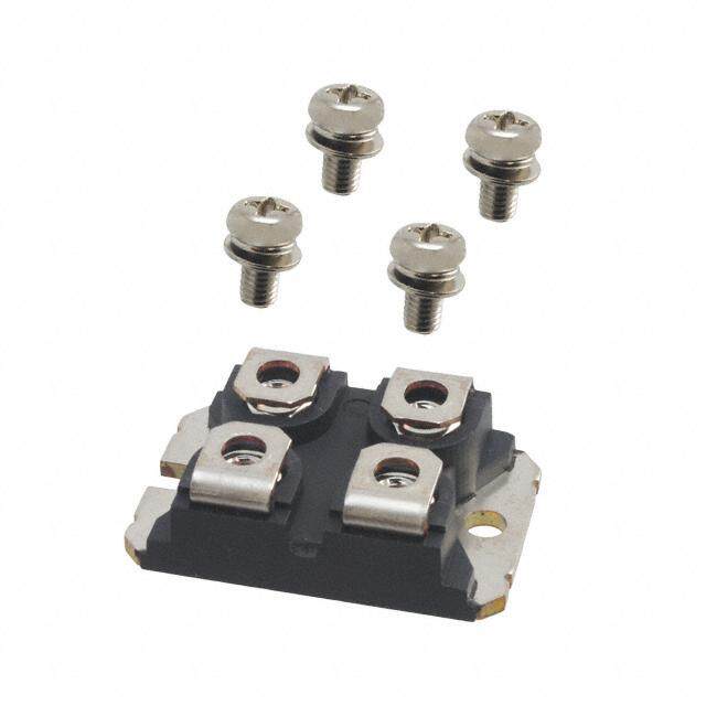
| 产品图片 |
|
| rohs | 符合RoHS无铅 / 符合限制有害物质指令(RoHS)规范要求 |
| 产品系列 | 晶体管,MOSFET,NXP Semiconductors BUK7528-55A,127TrenchMOS™ |
| 数据手册 | |
| 产品型号 | BUK7528-55A,127 |
| Pd-PowerDissipation | 99 W |
| Pd-功率耗散 | 99 W |
| RdsOn-Drain-SourceResistance | 28 mOhms |
| RdsOn-漏源导通电阻 | 28 mOhms |
| Vds-Drain-SourceBreakdownVoltage | 55 V |
| Vds-漏源极击穿电压 | 55 V |
| Vgs-Gate-SourceBreakdownVoltage | +/- 20 V |
| Vgs-栅源极击穿电压 | 20 V |
| 上升时间 | 68 ns |
| 下降时间 | 43 ns |
| 不同Id时的Vgs(th)(最大值) | 4V @ 1mA |
| 不同Vds时的输入电容(Ciss) | 1165pF @ 25V |
| 不同Vgs时的栅极电荷(Qg) | - |
| 不同 Id、Vgs时的 RdsOn(最大值) | 28 毫欧 @ 25A,10V |
| 产品种类 | MOSFET |
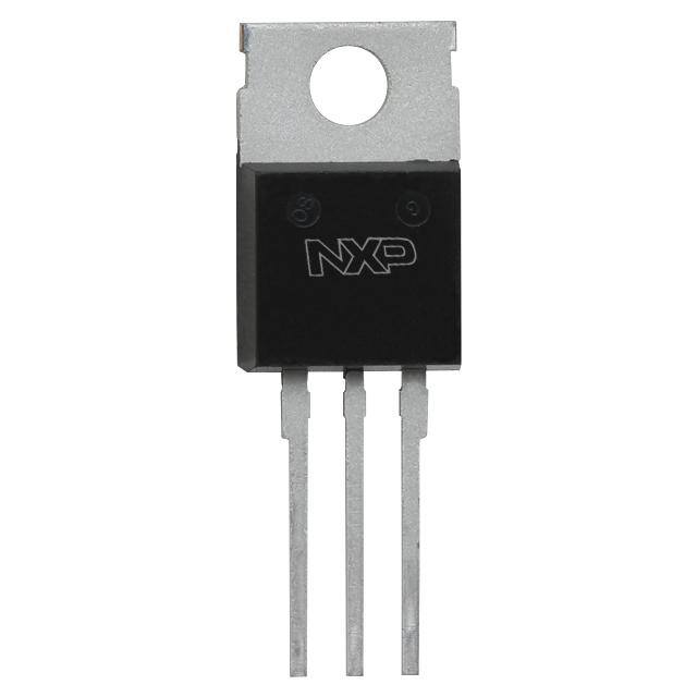
| 供应商器件封装 | TO-220AB |
| 其它名称 | 568-9799-5 |
| 典型关闭延迟时间 | 83 ns |
| 功率-最大值 | 99W |
| 包装 | 管件 |
| 商标 | NXP Semiconductors |
| 安装类型 | 通孔 |
| 安装风格 | Through Hole |
| 导通电阻 | 28 mOhms |
| 封装 | Tube |
| 封装/外壳 | TO-220-3 |
| 封装/箱体 | TO-220-3 |
| 工厂包装数量 | 1000 |
| 晶体管极性 | N-Channel |
| 最大工作温度 | + 175 C |
| 最小工作温度 | - 55 C |
| 标准包装 | 50 |
| 汲极/源极击穿电压 | 55 V |
| 漏极连续电流 | 42 A |
| 漏源极电压(Vdss) | 55V |
| 电流-连续漏极(Id)(25°C时) | 42A (Tmb) |
| 通道模式 | Enhancement |
| 配置 | Single |
| 零件号别名 | BUK7528-55A |


PDF Datasheet 数据手册内容提取
Important notice Dear Customer, On 7 February 2017 the former NXP Standard Product business became a new company with the tradename Nexperia. Nexperia is an industry leading supplier of Discrete, Logic and PowerMOS semiconductors with its focus on the automotive, industrial, computing, consumer and wearable application markets In data sheets and application notes which still contain NXP or Philips Semiconductors references, use the references to Nexperia, as shown below. Instead of http://www.nxp.com, http://www.philips.com/ or http://www.semiconductors.philips.com/, use http://www.nexperia.com Instead of sales.addresses@www.nxp.com or sales.addresses@www.semiconductors.philips.com, use salesaddresses@nexperia.com (email) Replace the copyright notice at the bottom of each page or elsewhere in the document, depending on the version, as shown below: - © NXP N.V. (year). All rights reserved or © Koninklijke Philips Electronics N.V. (year). All rights reserved Should be replaced with: - © Nexperia B.V. (year). All rights reserved. If you have any questions related to the data sheet, please contact our nearest sales office via e-mail or telephone (details via salesaddresses@nexperia.com). Thank you for your cooperation and understanding, Kind regards, Team Nexperia
BUK7528-55A TO-220AB N-channel TrenchMOS standard level FET Rev. 02 — 21 April 2011 Product data sheet 1. Product profile 1.1 General description Standard level N-channel enhancement mode Field-Effect Transistor (FET) in a plastic package using TrenchMOS technology. This product has been designed and qualified to the appropriate AEC standard for use in automotive critical applications. 1.2 Features and benefits (cid:132) AEC Q101 compliant (cid:132) Low conduction losses due to low on-state resistance 1.3 Applications (cid:132) Automotive and general purpose power switching 1.4 Quick reference data Table 1. Quick reference data Symbol Parameter Conditions Min Typ Max Unit V drain-source voltage T ≥25°C; T ≤175°C - - 55 V DS j j I drain current T =25°C - - 42 A D mb P total power dissipation - - 99 W tot Static characteristics R drain-source on-state V =10V; I =25A; - 23.8 28 mΩ DSon GS D resistance T =25°C j Avalanche ruggedness E non-repetitive I =34A; V ≤25V; - - 58 mJ DS(AL)S D sup drain-source avalanche R =50Ω; V =5V; GS GS energy T =25°C; unclamped j(init)
BUK7528-55A NXP Semiconductors N-channel TrenchMOS standard level FET 2. Pinning information Table 2. Pinning infor mation Pin Symbol Description Simplified outline Graphic symbol 1 G gate mb D 2 D drain 3 S source G mb D mounting base; connected to drain mbb076 S 1 2 3 SOT78A (TO-220AB) 3. Ordering information Table 3. Ordering info rmation Type number Package Name Description Version BUK7528-55A TO-220AB plastic single-ended package; heatsink mounted; 1 mounting SOT78A hole; 3-lead TO-220AB 4. Limiting values Table 4. Limiting valu es In accordance with the Absolute Maximum Rating System (IEC 60134). Symbol Parameter Conditions Min Max Unit V drain-source voltage T ≥25°C; T ≤175°C - 55 V DS j j V drain-gate voltage R =20kΩ - 55 V DGR GS V gate-source voltage -20 20 V GS I drain current T =25°C - 42 A D mb T =100°C - 30 A mb I peak drain current T =25°C; pulsed - 168 A DM mb P total power dissipation T =25°C - 99 W tot mb T storage temperature -55 175 °C stg T junction temperature -55 175 °C j Source-drain diode I source current T =25°C - 41 A S mb I peak source current pulsed; T =25°C - 163 A SM mb Avalanche ruggedness E non-repetitive drain-source I =34A; V ≤25V; R =50Ω; - 58 mJ DS(AL)S D sup GS avalanche energy V =5V; T =25°C; unclamped GS j(init) BUK7528-55A All information provided in this document is subject to legal disclaimers. © NXP B.V. 2011. All rights reserved. Product data sheet Rev. 02 — 21 April 2011 2 of 13
BUK7528-55A NXP Semiconductors N-channel TrenchMOS standard level FET 003aaf455 003aaf456 100 100 Pder ID (%) (%) 80 80 60 60 40 40 20 20 0 0 0 50 100 150 200 0 50 100 150 200 Tmb (°C) Tmb (°C) V ≥ 5 V GS Fig 1. Normalized total power dissipation as a Fig 2. Normalized continuous drain current as a function of mounting base temperature function of mounting base temperature 103 003aaf457 100 003aaf470 (IAD) RDS(on) = VDS / ID W(%DS)8S0 102 tp = 10 μs 60 100 μs 40 10 1 ms D.C. 20 10 ms 100 ms 1 0 1 10 102 103 20 60 100 140 180 VDS (V) Tmb (°C) T = 25 °C; I is single pulse I = 75 A mb DM D Fig 3. Safe operating area; continuous and peak drain Fig 4. Normalised drain-source non-repetitive currents as a function of drain-source voltage avalanche energy as a function of mounting-base temperature BUK7528-55A All information provided in this document is subject to legal disclaimers. © NXP B.V. 2011. All rights reserved. Product data sheet Rev. 02 — 21 April 2011 3 of 13
BUK7528-55A NXP Semiconductors N-channel TrenchMOS standard level FET 5. Thermal characteristics Table 5. Thermal cha racteristics Symbol Parameter Conditions Min Typ Max Unit R thermal resistance from junction to mounting - - 1.5 K/W th(j-mb) base R thermal resistance from junction to ambient in free air - 60 - K/W th(j-a) 003aaf458 10 Zth(j-mb) (K/W) 1 δ = 0.5 00..21 P δ = Ttp 10−1 0.05 0.02 0 tp t T 10−2 10−6 10−4 10−2 1 102 104 tp (s) Fig 5. Transient thermal impedance from junction to mounting base as a function of pulse duration BUK7528-55A All information provided in this document is subject to legal disclaimers. © NXP B.V. 2011. All rights reserved. Product data sheet Rev. 02 — 21 April 2011 4 of 13
BUK7528-55A NXP Semiconductors N-channel TrenchMOS standard level FET 6. Characteristics Table 6. Characterist ics Symbol Parameter Conditions Min Typ Max Unit Static characteristics V drain-source breakdown I =0.25mA; V =0V; T =25°C 55 - - V (BR)DSS D GS j voltage I =0.25mA; V =0V; T =-55°C 50 - - V D GS j V gate-source threshold I =1mA; V =V ; T =-55°C - - 4.4 V GS(th) D DS GS j voltage I =1mA; V =V ; T =25°C 2 3 4 V D DS GS j I =1mA; V =V ; T =175°C 1 - - V D DS GS j I drain leakage current V =55V; V =0V; T =25°C - 0.05 10 µA DSS DS GS j V =55V; V =0V; T =175°C - - 500 µA DS GS j I gate leakage current V =20V; V =0V; T =25°C - 2 100 nA GSS GS DS j V =-20V; V =0V; T =25°C - 2 100 nA GS DS j R drain-source on-state V =10V; I =25A; T =175°C - - 56 mΩ DSon GS D j resistance V =10V; I =25A; T =25°C - 23.8 28 mΩ GS D j Dynamic characteristics C input capacitance V =0V; V =25V; f=1MHz; - 874 1165 pF iss GS DS T =25°C C output capacitance j - 218 261 pF oss C reverse transfer capacitance - 137 188 pF rss t turn-on delay time V =30V; R =1.2Ω; V =5V; - 14 21 ns d(on) DS L GS R =10Ω; T =25°C t rise time G(ext) j - 68 102 ns r t turn-off delay time - 83 116 ns d(off) t fall time - 43 60 ns f L internal drain inductance measured from drain lead 6 mm from - 4.5 - nH D package to centre of die; T =25°C j measured from contact screw on tab - 3.5 - nH to centre of die; T =25°C j L internal source inductance measured from source lead to source - 7.5 - nH S bond pad; T =25°C j Source-drain diode V source-drain voltage I =41A; V =0V; T =25°C - 1.1 - V SD S GS j I =25A; V =0V; T =25°C - 0.85 1.2 V S GS j t reverse recovery time I =20A; dI /dt=-100A/µs; - 45 50 ns rr S S V =-10V; V =30V; T =25°C Q recovered charge GS DS j - 88 96 nC r BUK7528-55A All information provided in this document is subject to legal disclaimers. © NXP B.V. 2011. All rights reserved. Product data sheet Rev. 02 — 21 April 2011 5 of 13
BUK7528-55A NXP Semiconductors N-channel TrenchMOS standard level FET 003aaf459 003aaf460 100 70 ID 18 10 RDS(on) 6 (A) 16 9.5 (mΩ) 80 12 10.5 9.0 60 6.5 11.5 VGS (V) = 11 8.5 7 60 8.0 50 7.5 8 7.0 40 40 6.5 9 6.0 20 30 10 5.5 5.0 4.5 0 20 0 2 4 6 8 10 0 20 40 60 80 100 VDS (V) ID (A) T = 25 °C T = 25 °C j j Fig 6. Output characteristics: drain current as a Fig 7. Drain-source on-state resistance as a function function of drain-source voltage; typical values of drain current; typical values 003aaf461 003aaf462 50 100 RDS(on) (IAD) (mΩ) 80 40 60 30 40 20 20 Tj = 175 °C Tj = 25 °C 10 0 6 10 14 18 22 0 4 8 12 VGS (V) VGS (V) T = 25 °C; I = 25 A V > I x R j D DS D DSon Fig 8. Drain-source on-state resistance as a function Fig 9. Transfer characteristics: drain current as a of gate-source voltage; typical values function of gate-source voltage; typical values BUK7528-55A All information provided in this document is subject to legal disclaimers. © NXP B.V. 2011. All rights reserved. Product data sheet Rev. 02 — 21 April 2011 6 of 13
BUK7528-55A NXP Semiconductors N-channel TrenchMOS standard level FET 003aaf463 003aaf464 16 2.5 gfs a (S) 12 2 8 1.5 4 1 0 0.5 0 20 40 60 80 −100 0 100 200 ID (A) Tmb (°C) V > I x R DS D DSon I = 25 A; V = 5 V D GS Fig 10. Forward transconductance as a function of Fig 11. Normalized drain-source on-state resistance drain current; typical values factor as a function of junction temperature 5 003aaf465 10−1 003aaf466 VGS(th) ID (V) (A) 4 maximum 10−2 3 typical 10−3 2 minimum 10−4 2 % typical 98 % 1 10−5 0 10−6 −100 0 100 200 0 1 2 3 4 5 Tj (°C) VGS (V) I = 1 mA; V = V T = 25 °C; V = V D DS GS j DS GS Fig 12. Gate-source threshold voltage as a function of Fig 13. Sub-threshold drain current as a function of junction temperature gate-source voltage BUK7528-55A All information provided in this document is subject to legal disclaimers. © NXP B.V. 2011. All rights reserved. Product data sheet Rev. 02 — 21 April 2011 7 of 13
BUK7528-55A NXP Semiconductors N-channel TrenchMOS standard level FET 003aaf467 003aaf468 1.6 10 C VGS (nF) Ciss (V) 8 1.2 VDS = 14 V VDS = 44 V 6 Coss 0.8 4 0.4 Crss 2 0.0 0 10−2 10−1 1 10 102 0 10 20 30 VDS (V) QG (nC) V = 0 V; f = 1 MHz T = 25 °C; I = 50 A GS j D Fig 14. Input, output and reverse transfer capacitances Fig 15. Gate-source voltage as a function of gate as a function of drain-source voltage; typical charge; typical values values 003aaf469 120 IF (A) 80 40 Tj = 175 °C Tj = 25 °C 0 0.0 0.5 1.0 1.5 VSDS (V) V = 0 V GS Fig 16. Source (diode forward) current as a function of source-drain (diode forward) voltage; typical values BUK7528-55A All information provided in this document is subject to legal disclaimers. © NXP B.V. 2011. All rights reserved. Product data sheet Rev. 02 — 21 April 2011 8 of 13
BUK7528-55A NXP Semiconductors N-channel TrenchMOS standard level FET 7. Package outline Plastic single-ended package; heatsink mounted; 1 mounting hole; 3-lead TO-220AB SOT78A E A p A1 q mounting D1 base D L1(1) L2 Q b1 L 1 2 3 b c e e 0 5 10 mm scale DIMENSIONS (mm are the original dimensions) UNIT A A1 b b1 c D D1 E e L L1(1) mLa2x. p q Q 4.5 1.39 0.9 1.3 0.7 15.8 6.4 10.3 15.0 3.30 3.8 3.0 2.6 mm 2.54 3.0 4.1 1.27 0.6 1.0 0.4 15.2 5.9 9.7 13.5 2.79 3.6 2.7 2.2 Note 1. Terminals in this zone are not tinned. OUTLINE REFERENCES EUROPEAN ISSUE DATE VERSION IEC JEDEC JEITA PROJECTION 03-01-22 SOT78A 3-lead TO-220AB SC-46 05-03-14 Fig 17. Package outline SOT78A (TO-220AB) BUK7528-55A All information provided in this document is subject to legal disclaimers. © NXP B.V. 2011. All rights reserved. Product data sheet Rev. 02 — 21 April 2011 9 of 13
BUK7528-55A NXP Semiconductors N-channel TrenchMOS standard level FET 8. Revision history Table 7. Revision his tory Document ID Release date Data sheet status Change notice Supersedes BUK7528-55A v.2 20110421 Product data sheet - BUK7528_7628-55A v.1 Modifications: • The format of this data sheet has been redesigned to comply with the new identity guidelines of NXP Semiconductors. • Legal texts have been adapted to the new company name where appropriate. • Type number BUK7528-55A separated from data sheet BUK7528_7628-55A v.1. BUK7528_7628-55A v.1 20000601 Product specification - - BUK7528-55A All information provided in this document is subject to legal disclaimers. © NXP B.V. 2011. All rights reserved. Product data sheet Rev. 02 — 21 April 2011 10 of 13
BUK7528-55A NXP Semiconductors N-channel TrenchMOS standard level FET 9. Legal information 9.1 Data sheet status Document status [1] [2] Product status [3] Definition Objective [short] data sheet Development This document contains data from the objective specification for product development. Preliminary [short] data sheet Qualification This document contains data from the preliminary specification. Product [short] data sheet Production This document contains the product specification. [1] Please consult the most recently issued document before initiating or completing a design. [2] The term 'short data sheet' is explained in section "Definitions". [3] The product status of device(s) described in this document may have changed since this document was published and may differ in case of multiple devices. The latest product status information is available on the Internet at URL http://www.nxp.com. 9.2 Definitions Right to make changes — NXP Semiconductors reserves the right to make changes to information published in this document, including without Preview — The document is a preview version only. The document is still limitation specifications and product descriptions, at any time and without subject to formal approval, which may result in modifications or additions. notice. This document supersedes and replaces all information supplied prior NXP Semiconductors does not give any representations or warranties as to to the publication hereof. the accuracy or completeness of information included herein and shall have no liability for the consequences of use of such information. Suitability for use in automotive applications — This NXP Semiconductors product has been qualified for use in automotive Draft — The document is a draft version only. The content is still under applications. The product is not designed, authorized or warranted to be internal review and subject to formal approval, which may result in suitable for use in medical, military, aircraft, space or life support equipment, modifications or additions. NXP Semiconductors does not give any nor in applications where failure or malfunction of an NXP Semiconductors representations or warranties as to the accuracy or completeness of product can reasonably be expected to result in personal injury, death or information included herein and shall have no liability for the consequences of severe property or environmental damage. NXP Semiconductors accepts no use of such information. liability for inclusion and/or use of NXP Semiconductors products in such equipment or applications and therefore such inclusion and/or use is at the Short data sheet — A short data sheet is an extract from a full data sheet customer’s own risk. with the same product type number(s) and title. A short data sheet is intended for quick reference only and should not be relied upon to contain detailed and Quick reference data — The Quick reference data is an extract of the full information. For detailed and full information see the relevant full data product data given in the Limiting values and Characteristics sections of this sheet, which is available on request via the local NXP Semiconductors sales document, and as such is not complete, exhaustive or legally binding. office. In case of any inconsistency or conflict with the short data sheet, the full data sheet shall prevail. Applications — Applications that are described herein for any of these products are for illustrative purposes only. NXP Semiconductors makes no Product specification — The information and data provided in a Product representation or warranty that such applications will be suitable for the data sheet shall define the specification of the product as agreed between specified use without further testing or modification. NXP Semiconductors and its customer, unless NXP Semiconductors and customer have explicitly agreed otherwise in writing. In no event however, Customers are responsible for the design and operation of their applications shall an agreement be valid in which the NXP Semiconductors product is and products using NXP Semiconductors products, and NXP Semiconductors deemed to offer functions and qualities beyond those described in the accepts no liability for any assistance with applications or customer product Product data sheet. design. It is customer’s sole responsibility to determine whether the NXP Semiconductors product is suitable and fit for the customer’s applications and products planned, as well as for the planned application and use of 9.3 Disclaimers customer’s third party customer(s). Customers should provide appropriate design and operating safeguards to minimize the risks associated with their Limited warranty and liability — Information in this document is believed to applications and products. be accurate and reliable. However, NXP Semiconductors does not give any representations or warranties, expressed or implied, as to the accuracy or NXP Semiconductors does not accept any liability related to any default, completeness of such information and shall have no liability for the damage, costs or problem which is based on any weakness or default in the consequences of use of such information. customer’s applications or products, or the application or use by customer’s third party customer(s). Customer is responsible for doing all necessary In no event shall NXP Semiconductors be liable for any indirect, incidental, testing for the customer’s applications and products using NXP punitive, special or consequential damages (including - without limitation - lost Semiconductors products in order to avoid a default of the applications and profits, lost savings, business interruption, costs related to the removal or the products or of the application or use by customer’s third party replacement of any products or rework charges) whether or not such customer(s). NXP does not accept any liability in this respect. damages are based on tort (including negligence), warranty, breach of contract or any other legal theory. Limiting values — Stress above one or more limiting values (as defined in the Absolute Maximum Ratings System of IEC 60134) will cause permanent Notwithstanding any damages that customer might incur for any reason damage to the device. Limiting values are stress ratings only and (proper) whatsoever, NXP Semiconductors’ aggregate and cumulative liability towards operation of the device at these or any other conditions above those given in customer for the products described herein shall be limited in accordance the Recommended operating conditions section (if present) or the with the Terms and conditions of commercial sale of NXP Semiconductors. BUK7528-55A All information provided in this document is subject to legal disclaimers. © NXP B.V. 2011. All rights reserved. Product data sheet Rev. 02 — 21 April 2011 11 of 13
BUK7528-55A NXP Semiconductors N-channel TrenchMOS standard level FET Characteristics sections of this document is not warranted. Constant or Export control — This document as well as the item(s) described herein may repeated exposure to limiting values will permanently and irreversibly affect be subject to export control regulations. Export might require a prior the quality and reliability of the device. authorization from national authorities. Terms and conditions of commercial sale — NXP Semiconductors 9.4 Trademarks products are sold subject to the general terms and conditions of commercial sale, as published at http://www.nxp.com/profile/terms, unless otherwise agreed in a valid written individual agreement. In case an individual Notice: All referenced brands, product names, service names and trademarks agreement is concluded only the terms and conditions of the respective are the property of their respective owners. agreement shall apply. NXP Semiconductors hereby expressly objects to applying the customer’s general terms and conditions with regard to the Adelante, Bitport, Bitsound, CoolFlux, CoReUse, DESFire, EZ-HV, purchase of NXP Semiconductors products by customer. FabKey, GreenChip, HiPerSmart, HITAG, I²C-bus logo, ICODE, I-CODE, ITEC, Labelution, MIFARE, MIFARE Plus, MIFARE Ultralight, MoReUse, No offer to sell or license — Nothing in this document may be interpreted or QLPAK, Silicon Tuner, SiliconMAX, SmartXA, STARplug, TOPFET, construed as an offer to sell products that is open for acceptance or the grant, TrenchMOS, TriMedia and UCODE — are trademarks of NXP B.V. conveyance or implication of any license under any copyrights, patents or other industrial or intellectual property rights. HD Radio and HD Radio logo — are trademarks of iBiquity Digital Corporation. 10. Contact information For more information, please visit: http://www.nxp.com For sales office addresses, please send an email to: salesaddresses@nxp.com BUK7528-55A All information provided in this document is subject to legal disclaimers. © NXP B.V. 2011. All rights reserved. Product data sheet Rev. 02 — 21 April 2011 12 of 13
BUK7528-55A NXP Semiconductors N-channel TrenchMOS standard level FET 11. Contents 1 Product profile. . . . . . . . . . . . . . . . . . . . . . . . . . .1 1.1 General description . . . . . . . . . . . . . . . . . . . . . .1 1.2 Features and benefits. . . . . . . . . . . . . . . . . . . . .1 1.3 Applications . . . . . . . . . . . . . . . . . . . . . . . . . . . .1 1.4 Quick reference data . . . . . . . . . . . . . . . . . . . . .1 2 Pinning information. . . . . . . . . . . . . . . . . . . . . . .2 3 Ordering information. . . . . . . . . . . . . . . . . . . . . .2 4 Limiting values. . . . . . . . . . . . . . . . . . . . . . . . . . .2 5 Thermal characteristics . . . . . . . . . . . . . . . . . . .4 6 Characteristics. . . . . . . . . . . . . . . . . . . . . . . . . . .5 7 Package outline. . . . . . . . . . . . . . . . . . . . . . . . . .9 8 Revision history. . . . . . . . . . . . . . . . . . . . . . . . .10 9 Legal information. . . . . . . . . . . . . . . . . . . . . . . .11 9.1 Data sheet status . . . . . . . . . . . . . . . . . . . . . . .11 9.2 Definitions. . . . . . . . . . . . . . . . . . . . . . . . . . . . .11 9.3 Disclaimers. . . . . . . . . . . . . . . . . . . . . . . . . . . .11 9.4 Trademarks. . . . . . . . . . . . . . . . . . . . . . . . . . . .12 10 Contact information. . . . . . . . . . . . . . . . . . . . . .12 Please be aware that important notices concerning this document and the product(s) described herein, have been included in section ‘Legal information’. © NXP B.V. 2011. All rights reserved. For more information, please visit: http://www.nxp.com For sales office addresses, please send an email to: salesaddresses@nxp.com Date of release: 21 April 2011 Document identifier: BUK7528-55A