ICGOO在线商城 > 分立半导体产品 > 晶体管 - FET,MOSFET - 单 > BSC046N10NS3GATMA1

 Datasheet下载
- 型号: BSC046N10NS3GATMA1
- 制造商: Infineon
- 库位|库存: xxxx|xxxx
- 要求:
| 数量阶梯 | 香港交货 | 国内含税 |
| +xxxx | $xxxx | ¥xxxx |
查看当月历史价格
查看今年历史价格
BSC046N10NS3GATMA1产品简介:
ICGOO电子元器件商城为您提供BSC046N10NS3GATMA1由Infineon设计生产,在icgoo商城现货销售,并且可以通过原厂、代理商等渠道进行代购。 BSC046N10NS3GATMA1价格参考。InfineonBSC046N10NS3GATMA1封装/规格:晶体管 - FET,MOSFET - 单, N-Channel 100V 17A (Ta), 100A (Tc) 156W (Tc) Surface Mount PG-TDSON-8-7。您可以下载BSC046N10NS3GATMA1参考资料、Datasheet数据手册功能说明书,资料中有BSC046N10NS3GATMA1 详细功能的应用电路图电压和使用方法及教程。
Infineon Technologies 的 BSC046N10NS3GATMA1 是一款N沟道功率MOSFET,属于OptiMOS™系列,具有100V耐压和低导通电阻(RDS(on)),适用于高效率、高密度的电源转换应用。该器件采用先进的沟槽技术,在性能和可靠性方面表现优异。

主要应用场景包括:

1. 开关电源(SMPS):广泛用于服务器、通信设备和工业电源中的DC-DC转换器,因其低导通损耗和高开关效率,有助于提升整体能效。

2. 电动工具与电池管理系统:适用于锂电驱动设备中的功率开关,如电动工具、电动自行车及储能系统,支持大电流开关操作,提高电池利用率。

3. 电机驱动:在工业自动化、家用电器(如变频空调、洗衣机)的电机控制电路中,作为主开关元件,实现高效节能运行。

4. 照明电源:用于LED驱动电源,特别是在高功率LED照明系统中,提供稳定可靠的功率控制。

5. 新能源领域:可应用于太阳能逆变器和电动汽车车载充电机(OBC)中的辅助电源模块,满足高温和高可靠性的要求。

BSC046N10NS3GATMA1 采用PG-TSDS-8 封装,具备良好的热性能和紧凑尺寸,适合空间受限的高密度PCB设计。其优化的栅极电荷和低反向恢复电荷,有效降低开关损耗,提升系统效率,是中高功率应用的理想选择。
| 参数 | 数值 |
| 产品目录 | |
| 描述 | MOSFET N-CH 100V 100A TDSON-8 |
| 产品分类 | FET - 单 |
| FET功能 | 逻辑电平门 |
| FET类型 | MOSFET N 通道,金属氧化物 |
| 品牌 | Infineon Technologies |
| 数据手册 | http://www.infineon.com/dgdl/BSC046N10NS3+Rev2.0.pdf?folderId=db3a304313b8b5a60113cee8763b02d7&fileId=db3a304332fc1ee7013316f966a4713c |
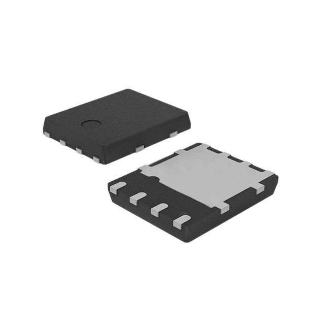
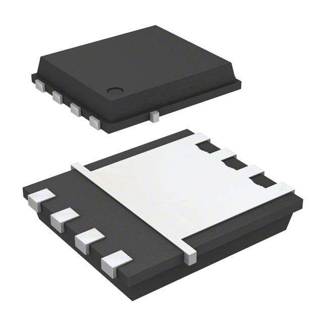
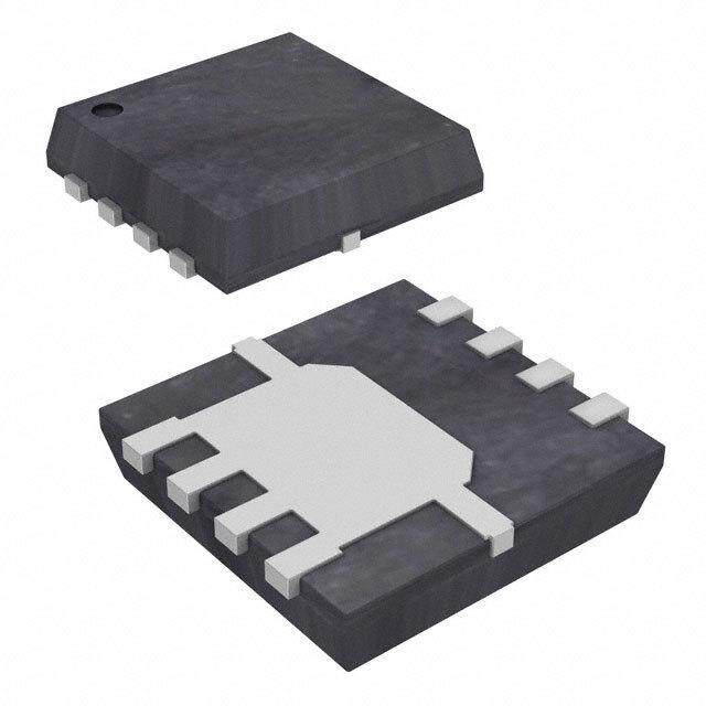
| 产品图片 |
|
| 产品型号 | BSC046N10NS3GATMA1 |
| PCN其它 | |
| rohs | 无铅 / 符合限制有害物质指令(RoHS)规范要求 |
| 产品系列 | OptiMOS™ |
| 不同Id时的Vgs(th)(最大值) | 3.5V @ 120µA |
| 不同Vds时的输入电容(Ciss) | 4500pF @ 50V |
| 不同Vgs时的栅极电荷(Qg) | 63nC @ 10V |
| 不同 Id、Vgs时的 RdsOn(最大值) | 4.6 毫欧 @ 50A,10V |
| 供应商器件封装 | PG-TDSON-8(5.15x6.15) |
| 其它名称 | BSC046N10NS3GATMA1TR |
| 功率-最大值 | 156W |
| 包装 | 带卷 (TR) |
| 安装类型 | 表面贴装 |
| 封装/外壳 | 8-PowerTDFN |
| 标准包装 | 5,000 |
| 漏源极电压(Vdss) | 100V |
| 电流-连续漏极(Id)(25°C时) | 17A (Ta), 100A (Tc) |


- 商务部:美国ITC正式对集成电路等产品启动337调查
- 曝三星4nm工艺存在良率问题 高通将骁龙8 Gen1或转产台积电
- 太阳诱电将投资9.5亿元在常州建新厂生产MLCC 预计2023年完工
- 英特尔发布欧洲新工厂建设计划 深化IDM 2.0 战略
- 台积电先进制程称霸业界 有大客户加持明年业绩稳了
- 达到5530亿美元!SIA预计今年全球半导体销售额将创下新高
- 英特尔拟将自动驾驶子公司Mobileye上市 估值或超500亿美元
- 三星加码芯片和SET,合并消费电子和移动部门,撤换高东真等 CEO
- 三星电子宣布重大人事变动 还合并消费电子和移动部门
- 海关总署:前11个月进口集成电路产品价值2.52万亿元 增长14.8%


PDF Datasheet 数据手册内容提取
BSC046N10NS3 G OptiMOSTM3 Power-Transistor ProductSummary Features V 100 V DS •Verylowgatechargeforhighfrequencyapplications R 4.6 mW DS(on),max •Optimizedfordc-dcconversion I 100 A D •N-channel,normallevel PG-TDSON-8 •ExcellentgatechargexR product(FOM) DS(on) •Verylowon-resistanceR DS(on) •150°Coperatingtemperature •Pb-freeleadplating;RoHScompliant •QualifiedaccordingtoJEDEC1)fortargetapplication •Halogen-freeaccordingtoIEC61249-2-21 Type Package Marking BSC046N10NS3 G PG-TDSON-8 046N10NS MMaaxxiimmuummrraattiinnggss,,aattTT ==2255°°CC,,uunnlleessssootthheerrwwiisseessppeecciiffiieedd j Parameter Symbol Conditions Value Unit Continuousdraincurrent I T =25°C 100 A D C T =100°C 85 C T =25°C, A 17.0 R =50K/W2) thJA Pulseddraincurrent3) ID,pulse TC=25°C 400 Avalancheenergy,singlepulse E I =50A,R =25W 350 mJ AS D GS Gatesourcevoltage V ±20 V GS Powerdissipation P T =25°C 156 W tot C Operatingandstoragetemperature T ,T -55...150 °C j stg IECclimaticcategory;DINIEC68-1 55/150/56 RReevv..22..00 ppaaggee11 22001111--0099--2299
BSC046N10NS3 G Parameter Symbol Conditions Values Unit min. typ. max. Thermalcharacteristics Thermalresistance,junction-case R - - 0.8 K/W thJC R minimalfootprint - - 62 Thermalresistance, thJA junction-ambient 6cm2coolingarea2) - - 50 Electricalcharacteristics,atT =25°C,unlessotherwisespecified j Staticcharacteristics Drain-sourcebreakdownvoltage V V =0V,I =1mA 100 - - V (BR)DSS GS D Gatethresholdvoltage V V =V ,I =120µA 2 2.7 3.5 GS(th) DS GS D V =100V,V =0V, Zerogatevoltagedraincurrent I DS GS - 0.01 1 µA DSS T =25°C j V =100V,V =0V, DS GS - 10 100 T =125°C j Gate-sourceleakagecurrent I V =20V,V =0V - 1 100 nA GSS GS DS Drain-sourceon-stateresistance R V =10V,I =50A - 4 4.6 mW DS(on) GS D V =6V,I =25A - 5.1 8.6 GS D Gateresistance R - 1.9 - W G |V |>2|I |R , Transconductance g DS D DS(on)max 48 96 - S fs I =50A D 1)J-STD20andJESD22 2)Deviceon40mmx40mmx1.5mmepoxyPCBFR4with6cm2(onelayer,70µmthick)copperareafordrain connection.PCBisverticalinstillair. 3)seefigure3 RReevv..22..00 ppaaggee22 22001111--0099--2299
BSC046N10NS3 G Parameter Symbol Conditions Values Unit min. typ. max. Dynamiccharacteristics Inputcapacitance C - 4500 - pF iss V =0V,V =50V, Outputcapacitance C GS DS - 790 - oss f=1MHz Reversetransfercapacitance C - 30 - rss Turn-ondelaytime t - 16 - ns d(on) Risetime tr V =50V,V =10V, - 14 - DD GS I =25A,R =1.6W Turn-offdelaytime t D G - 41 - d(off) Falltime t - 11 - f GateChargeCharacteristics4) Gatetosourcecharge Q - 20 - nC gs Gatetodraincharge Q - 11 - gd V =50V,I =50A, Switchingcharge Q DD D - 19 - sw V =0to10V GS GGaatteecchhaarrggeettoottaall QQ -- 6633 -- gg Gateplateauvoltage V - 4.4 - V plateau Outputcharge Q V =50V,V =0V - 84 - nC oss DD GS ReverseDiode Diodecontinousforwardcurrent I - - 100 A S T =25°C C Diodepulsecurrent I - - 400 S,pulse V =0V,I =50A, Diodeforwardvoltage V GS F - 1 1.2 V SD T =25°C j Reverserecoverytime trr V =50V,I =25A, - 56 - ns R F di /dt=100A/µs Reverserecoverycharge Q F - 101 - nC rr 4)Seefigure16forgatechargeparameterdefinition RReevv..22..00 ppaaggee33 22001111--0099--2299
BSC046N10NS3 G 1Powerdissipation 2Draincurrent P =f(T ) I =f(T );V ≥10 V tot C D C GS 116600 111100 110000 114400 9900 112200 8800 110000 7700 [W][W] 8800 A]A] 6600 PPtottot I[I[DD 5500 6600 4400 3300 4400 2200 2200 1100 00 00 00 4400 8800 112200 116600 00 4400 8800 112200 116600 TT [[°°CC]] TT [[°°CC]] CC CC 3Safeoperatingarea 4Max.transientthermalimpedance I =f(V );T =25°C;D=0 Z =f(t ) D DS C thJC p parameter:t parameter:D=t /T p p 103 101 1µs 10µs 102 100 100µs ] W 1ms 0.5 A] 101 K/ [ [ D DC C I J Zth 0.2 0.1 10-1 0.05 100 0.02 0.01 singlepulse 10-1 10-2 10-1 100 101 102 103 10-5 10-4 10-3 10-2 10-1 100 V [V] t [s] DS p RReevv..22..00 ppaaggee44 22001111--0099--2299
BSC046N10NS3 G 5Typ.outputcharacteristics 6Typ.drain-sourceonresistance I =f(V );T =25°C R =f(I );T =25°C D DS j DS(on) D j parameter:V parameter:V GS GS 112200 1122 1100VV 66VV 77VV 55VV 110000 1100 44..55VV 8800 88 ]] WW 55VV mm A]A] 6600 [[ 66 I[I[DD S(on)S(on) 66VV DD 44..55VV RR 77VV 4400 44 1100VV 2200 22 00 00 00 11 22 33 00 2200 4400 6600 8800 110000 VV [[VV]] II [[AA]] DDSS DD 7Typ.transfercharacteristics 8Typ.forwardtransconductance I =f(V );|V |>2|I |R g =f(I );T =25°C D GS DS D DS(on)max fs D j parameter:T j 140 140 120 120 100 100 80 80 A] S] [ [ ID 60 gfs 60 40 40 150°C 20 25°C 20 0 0 0 2 4 6 0 20 40 60 80 100 V [V] I [A] GS D RReevv..22..00 ppaaggee55 22001111--0099--2299
BSC046N10NS3 G 9Drain-sourceon-stateresistance 10Typ.gatethresholdvoltage R =f(T );I =50A;V =10V V =f(T );V =V DS(on) j D GS GS(th) j GS DS parameter:I D 1100 44 33..55 88 33 11220000µµAA 22..55 ]] 66 112200µµAA WW mm V]V] [[ mmaaxx [[ n)n) h)h) 22 DS(oDS(o ttyypp GS(tGS(t RR 44 VV 11..55 11 22 00..55 00 00 --6600 --2200 2200 6600 110000 114400 118800 --6600 --2200 2200 6600 110000 114400 118800 TT [[°°CC]] TT [[°°CC]] jj jj 11Typ.capacitances 12Forwardcharacteristicsofreversediode C=f(V );V =0V;f=1MHz I =f(V ) DS GS F SD parameter:T j 104 1000 Ciss Coss 103 150°C,98% 25°C 100 ] pF 102 A] [ [ C Crss IF 150°C 10 101 25°C,98% 100 1 0 20 40 60 80 0 0.5 1 1.5 2 V [V] V [V] DS SD RReevv..22..00 ppaaggee66 22001111--0099--2299
BSC046N10NS3 G 13Avalanchecharacteristics 14Typ.gatecharge I =f(t );R =25W V =f(Q );I =50Apulsed AS AV GS GS gate D parameter:T parameter:V j(start) DD 110000 1100 5500VV 2200VV 8800VV 88 2255°°CC 110000°°CC 66 A]A] V]V] [[ 1100 [[ IIASAS 112255°°CC VVGSGS 44 22 11 00 11 1100 110000 11000000 00 1100 2200 3300 4400 5500 6600 7700 tt [[µµss]] QQ [[nnCC]] AAVV ggaattee 15Drain-sourcebreakdownvoltage 16Gatechargewaveforms V =f(T );I =1mA BR(DSS) j D 110 V GS Q g 105 V] [ SS) 100 D R( VB Vgs(th) 95 Qg(th) Qsw Qgate Q Q 90 gs gd -60 -40 -20 0 20 40 60 80 100 120 140 160 T [°C] j RReevv..22..00 ppaaggee77 22001111--0099--2299
BSC046N10NS3 G PackageOutline:PG-TDSON-8(SuperSO8) RReevv..22..00 ppaaggee88 22001111--0099--2299
BSC046N10NS3 G Dimensionsinmm RReevv..22..00 ppaaggee99 22001111--0099--2299
BSC046N10NS3 G Publishedby InfineonTechnologiesAG 81726Munich,Germany ©2011InfineonTechnologiesAG AllRightsReserved. LegalDisclaimer Theinformationgiveninthisdocumentshallinnoeventberegardedasaguaranteeof conditionsorcharacteristics.Withrespecttoanyexamplesorhintsgivenherein,anytypical valuesstatedhereinand/oranyinformationregardingtheapplicationofthedevice, InfineonTechnologiesherebydisclaimsanyandallwarrantiesandliabilitiesofanykind, iinncclluuddiinnggwwiitthhoouuttlliimmiittaattiioonn,,wwaarrrraannttiieessooffnnoonn--iinnffrriinnggeemmeennttooffiinntteelllleeccttuuaallpprrooppeerrttyyrriigghhttss ofanythirdparty. Information Forfurtherinformationontechnology,deliverytermsandconditionsandprices,please contactthenearestInfineonTechnologiesOffice(www.infineon.com). Warnings Duetotechnicalrequirements,componentsmaycontaindangeroussubstances.Forinformation onthetypesinquestion,pleasecontactthenearestInfineonTechnologiesOffice. InfineonTechnologiescomponentsmaybeusedinlife-supportdevicesorsystemsonlywith theexpresswrittenapprovalofInfineonTechnologies,ifafailureofsuchcomponentscan reasonablybeexpectedtocausethefailureofthatlife-supportdeviceorsystemortoaffect thesafetyoreffectivenessofthatdeviceorsystem.Lifesupportdevicesorsystemsare intendedtobeimplantedinthehumanbodyortosupportand/ormaintainandsustain and/orprotecthumanlife.Iftheyfail,itisreasonabletoassumethatthehealthoftheuser orotherpersonsmaybeendangered. RReevv..22..00 ppaaggee1100 22001111--0099--2299