ICGOO在线商城 > 分立半导体产品 > 晶体管 - FET,MOSFET - 单 > STS7NF60L
 Datasheet下载
- 型号: STS7NF60L
- 制造商: STMicroelectronics
- 库位|库存: xxxx|xxxx
- 要求:
| 数量阶梯 | 香港交货 | 国内含税 |
| +xxxx | $xxxx | ¥xxxx |
查看当月历史价格
查看今年历史价格
STS7NF60L产品简介:
ICGOO电子元器件商城为您提供STS7NF60L由STMicroelectronics设计生产,在icgoo商城现货销售,并且可以通过原厂、代理商等渠道进行代购。 STS7NF60L价格参考。STMicroelectronicsSTS7NF60L封装/规格:晶体管 - FET,MOSFET - 单, 表面贴装 N 沟道 60V 7.5A(Tc) 2.5W(Tc) 8-SO。您可以下载STS7NF60L参考资料、Datasheet数据手册功能说明书,资料中有STS7NF60L 详细功能的应用电路图电压和使用方法及教程。
STMicroelectronics的STS7NF60L是一款N沟道增强型MOSFET,其主要应用场景包括但不限于以下几个方面:

1. 开关电源(SMPS):STS7NF60L具有低导通电阻(Rds(on))和高击穿电压(600V),非常适合用于开关电源中的高频开关应用。它能够高效地控制功率传输,降低能量损耗。

2. 电机驱动:该MOSFET可用于各种电机驱动电路中,例如步进电机、直流无刷电机等。由于其出色的开关特性和耐压能力,可以稳定地控制电机的启动、停止和速度调节。

3. 逆变器:在太阳能逆变器或UPS系统中,STS7NF60L可以用作功率级开关元件,将直流电转换为交流电,同时保持较高的效率和可靠性。

4. DC-DC转换器:在需要高压输入的DC-DC转换器中,这款MOSFET可以作为主开关管使用,帮助实现高效的电压转换。

5. 负载开关和保护电路:利用其快速开关特性和低导通电阻,STS7NF60L适用于设计过流保护、短路保护以及负载切换电路,确保系统的安全运行。

6. 电动车和工业设备:在电动车的电池管理系统(BMS)、充电桩以及工业自动化设备中,这款器件能够承受高电压并提供稳定的电流控制。

总之,STS7NF60L凭借其优异的电气性能和耐用性,广泛应用于需要高效功率管理的各种电子产品和工业设备中。
| 参数 | 数值 |
| 产品目录 | |
| ChannelMode | Enhancement |
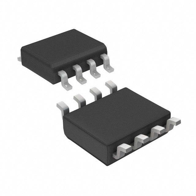
| 描述 | MOSFET N-CH 60V 7.5A 8-SOICMOSFET N-Ch 60 V 0.017 Ohm 7.5 A STripFET II |
| 产品分类 | FET - 单分离式半导体 |
| FET功能 | 逻辑电平门 |
| FET类型 | MOSFET N 通道,金属氧化物 |
| Id-ContinuousDrainCurrent | 7.5 A |
| Id-连续漏极电流 | 7.5 A |
| 品牌 | STMicroelectronics |
| 产品手册 | |
| 产品图片 |
|
| rohs | 符合RoHS无铅 / 符合限制有害物质指令(RoHS)规范要求 |
| 产品系列 | 晶体管,MOSFET,STMicroelectronics STS7NF60LSTripFET™ II |
| 数据手册 | |
| 产品型号 | STS7NF60L |
| Pd-PowerDissipation | 2.5 W |
| Pd-功率耗散 | 2.5 W |
| RdsOn-Drain-SourceResistance | 17 mOhms |
| RdsOn-漏源导通电阻 | 17 mOhms |
| Vds-Drain-SourceBreakdownVoltage | 60 V |
| Vds-漏源极击穿电压 | 60 V |
| Vgs-Gate-SourceBreakdownVoltage | +/- 16 V |
| Vgs-栅源极击穿电压 | 16 V |
| 上升时间 | 27 ns |
| 下降时间 | 20 ns |
| 不同Id时的Vgs(th)(最大值) | 1V @ 250µA |
| 不同Vds时的输入电容(Ciss) | 1700pF @ 25V |
| 不同Vgs时的栅极电荷(Qg) | 34nC @ 4.5V |
| 不同 Id、Vgs时的 RdsOn(最大值) | 19.5 毫欧 @ 3.5A,10V |
| 产品目录页面 | |
| 产品种类 | MOSFET |
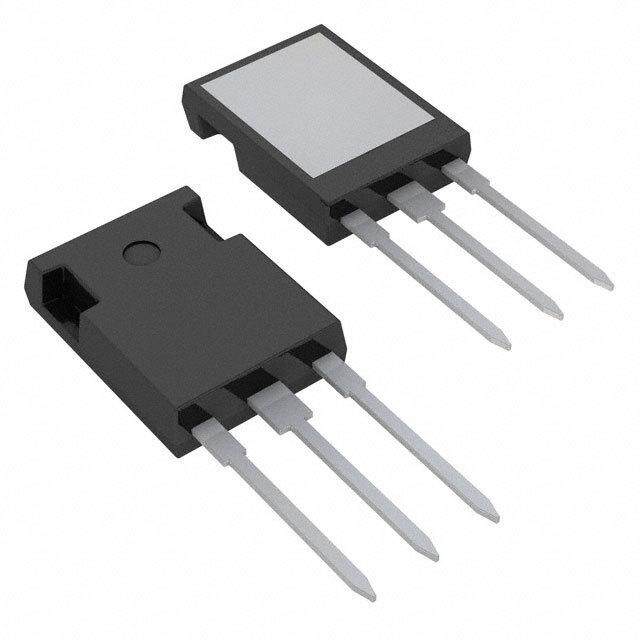
| 供应商器件封装 | 8-SO |
| 其它名称 | 497-4757-1 |
| 其它有关文件 | http://www.st.com/web/catalog/sense_power/FM100/CL824/SC1165/PF67473?referrer=70071840 |
| 典型关闭延迟时间 | 47 ns |
| 功率-最大值 | 2.5W |
| 包装 | 剪切带 (CT) |
| 商标 | STMicroelectronics |
| 安装类型 | 表面贴装 |
| 安装风格 | SMD/SMT |
| 封装 | Reel |
| 封装/外壳 | 8-SOIC(0.154",3.90mm 宽) |
| 封装/箱体 | SO-8 |
| 工厂包装数量 | 2500 |
| 晶体管极性 | N-Channel |
| 最大工作温度 | + 150 C |
| 最小工作温度 | - 55 C |
| 标准包装 | 1 |
| 漏源极电压(Vdss) | 60V |
| 电流-连续漏极(Id)(25°C时) | 7.5A (Tc) |
| 系列 | STS7NF60L |
| 通道模式 | Enhancement |
| 配置 | Single Quad Drain Triple Source |


- 商务部:美国ITC正式对集成电路等产品启动337调查
- 曝三星4nm工艺存在良率问题 高通将骁龙8 Gen1或转产台积电
- 太阳诱电将投资9.5亿元在常州建新厂生产MLCC 预计2023年完工
- 英特尔发布欧洲新工厂建设计划 深化IDM 2.0 战略
- 台积电先进制程称霸业界 有大客户加持明年业绩稳了
- 达到5530亿美元!SIA预计今年全球半导体销售额将创下新高
- 英特尔拟将自动驾驶子公司Mobileye上市 估值或超500亿美元
- 三星加码芯片和SET,合并消费电子和移动部门,撤换高东真等 CEO
- 三星电子宣布重大人事变动 还合并消费电子和移动部门
- 海关总署:前11个月进口集成电路产品价值2.52万亿元 增长14.8%


PDF Datasheet 数据手册内容提取
STS7NF60L W N-CHANNEL 60V - 0.017 - 7.5A SO-8 STripFET™ II POWER MOSFET TYPE VDSS RDS(on) ID STS7NF60L 60 V < 0.0195 W 7.5 A n TYPICAL RDS(on) = 0.017 W STANDARD OUTLINE FOR EASY n AUTOMATED SURFACE MOUNT ASSEMBLY LOW THRESHOLD DRIVE n DESCRIPTION This Power MOSFET is the latest development of STMicroelectronis unique "Single Feature Size™" SO-8 strip-based process. The resulting transistor shows extremely high packing density for low on- resistance, rugged avalanche characteristics and less critical alignment steps therefore a remark- able manufacturing reproducibility. INTERNAL SCHEMATIC DIAGRAM APPLICATIONS DC MOTOR DRIVE n DC-DC CONVERTERS n BATTERY MANAGEMENT IN NOMADIC n EQUIPMENT POWER MANAGEMENT IN n PORTABLE/DESKTOP PCs ABSOLUTE MAXIMUM RATINGS Symbol Parameter Value Unit VDS Drain-source Voltage (VGS = 0) 60 V VDGR Drain-gate Voltage (RGS = 20 kW ) 60 V VGS Gate- source Voltage ± 16 V ID Drain Current (continuous) at TC = 25°C 7.5 A ID Drain Current (continuous) at TC = 100°C 4.7 A IDM(•) Drain Current (pulsed) 30 A Ptot Total Dissipation at TC = 25°C 2.5 W EAS (1) Single Pulse Avalanche Energy 350 mJ (•) Pulse width limited by safe operating area. (1) Starting Tj = 25 oC, ID = 7.5 A VDD = 30 V April 2002 1/8 .
STS7NF60L THERMAL DATA Rthj-amb(#) Thermal Resistance Junction-ambient Max 50 °C/W Tj Maximum Operating Junction Temperature 150 °C Tstg Storage Temperature -55 to 150 °C (#) When Mounted on 1 inch2 FR-4 board, 2 oz of Cu and t [ 10 sec. ELECTRICAL CHARACTERISTICS (T = 25 °C unless otherwise specified) case OFF Symbol Parameter Test Conditions Min. Typ. Max. Unit V(BR)DSS DBrreaaink-dsoowurnc eV oltage ID = 250 µA, VGS = 0 60 V IDSS Zero Gate Voltage VDS = Max Rating 1 µA Drain Current (VGS = 0) VDS = Max Rating TC = 125°C 10 µA IGSS GCuartree-nbto (dVyD LSe =a k0a)ge VGS = ± 16 V ±100 nA ON (*) Symbol Parameter Test Conditions Min. Typ. Max. Unit VGS(th) Gate Threshold Voltage VDS = VGS ID = 250 µA 1 V RDS(on) Static Drain-source On VGS = 10 V ID = 3.5 A 0.017 0.0195 W Resistance VGS = 5 V ID = 3.5 A 0.019 0.0215 W DYNAMIC Symbol Parameter Test Conditions Min. Typ. Max. Unit gfs Forward Transconductance VDS = 15 V ID= 3.5 A 13 S Ciss Input Capacitance VDS = 25V, f = 1 MHz, VGS = 0 1700 pF Coss Output Capacitance 300 pF Crss Reverse Transfer 100 pF Capacitance 2/8
STS7NF60L ELECTRICAL CHARACTERISTICS (continued) SWITCHING ON (*) Symbol Parameter Test Conditions Min. Typ. Max. Unit td(on) Turn-on Delay Time VDD = 30 V ID = 3.5 A 15 ns tr Rise Time RG=4.7 W VGS = 4.5 V 27 ns (Resistive Load, Figure 1) Qg Total Gate Charge VDD= 48V ID 7.5A VGS=4.5V 25 34 nC Qgs Gate-Source Charge 4.5 nC Qgd Gate-Drain Charge (see test circuit, Figure 2) 7 nC SWITCHING OFF (*) Symbol Parameter Test Conditions Min. Typ. Max. Unit td(off) Turn-off Delay Time VDD = 30 V ID = 3.5 A 47 ns tf Fall Time RG=4.7W, VGS = 4.5 V 20 ns (Resistive Load, Figure 1) SOURCE DRAIN DIODE (*) Symbol Parameter Test Conditions Min. Typ. Max. Unit ISD Source-drain Current 7.5 A ISDM (•) Source-drain Current (pulsed) 30 A VSD Forward On Voltage ISD = 7.5 A VGS = 0 1.2 V trr Reverse Recovery Time ISD =7.5 A di/dt = 100A/µs 55 ns Qrr Reverse Recovery Charge VDD = 20 V Tj = 150°C 110 nC IRRM Reverse Recovery Current (see test circuit, Figure 3) 3.9 A (*) Pulse width [ 300 µs, duty cycle 1.5 %. (•)Pulse width limited by safe operating area. Safe Operating Area Thermal Impedance 3/8
STS7NF60L Output Characteristics Transfer Characteristics Transconductance Static Drain-source On Resistance Gate Charge vs Gate-source Voltage Capacitance Variations 4/8
STS7NF60L Normalized Gate Threshold Voltage vs Temperature Normalized on Resistance vs Temperature Source-drain Diode Forward Characteristics Normalized Breakdown Voltage vs Temperature . . 5/8
STS7NF60L FFiigg.. 11:: UUnnccllaammppeedd IInndduuccttiivvee LLooaadd TTeesstt CCiirrccuuiitt Fig. 2: Unclamped Inductive Waveform Fig. 3: Switching Times Test Circuits For Resistive Fig. 4: Gate Charge test Circuit Load Fig. 5: Test Circuit For Inductive Load Switching And Diode Recovery Times 6/8
STS7NF60L SO-8 MECHANICAL DATA mm inch DIM. MIN. TYP. MAX. MIN. TYP. MAX. A 1.75 0.068 a1 0.1 0.25 0.003 0.009 a2 1.65 0.064 a3 0.65 0.85 0.025 0.033 b 0.35 0.48 0.013 0.018 b1 0.19 0.25 0.007 0.010 C 0.25 0.5 0.010 0.019 c1 45 (typ.) D 4.8 5.0 0.188 0.196 E 5.8 6.2 0.228 0.244 e 1.27 0.050 e3 3.81 0.150 F 3.8 4.0 0.14 0.157 L 0.4 1.27 0.015 0.050 M 0.6 0.023 S 8 (max.) 0016023 7/8
STS7NF60L Information furnished is believed to be accurate and reliable. However, STMicroelectronics assumes no responsibility for the consequences of use of such information nor for any infringement of patents or other rights of third parties which may result from its use. No license is granted by implication or otherwise under any patent or patent rights of STMicroelectronics. Specifications mentioned in this publication are subject to change without notice. This publication supersedes and replaces all information previously supplied. STMicroelectronics products are not authorized for use as critical components in life support devices or systems without express written approval of STMicroelectronics. The ST logo is registered trademark of STMicroelectronics (cid:226) 2002 STMicroelectronics - All Rights Reserved All other names are the property of their respective owners. STMicroelectronics GROUP OF COMPANIES Australia - Brazil - Canada - China - Finland - France - Germany - Hong Kong - India - Israel - Italy - Japan - Malaysia - Malta - Morocco - Singapore - Spain - Sweden - Switzerland - United Kingdom - United States. http://www.st.com 8/8