ICGOO在线商城 > 分立半导体产品 > 晶体管 - FET,MOSFET - 单 > STP200NF04
 Datasheet下载
- 型号: STP200NF04
- 制造商: STMicroelectronics
- 库位|库存: xxxx|xxxx
- 要求:
| 数量阶梯 | 香港交货 | 国内含税 |
| +xxxx | $xxxx | ¥xxxx |
查看当月历史价格
查看今年历史价格
STP200NF04产品简介:
ICGOO电子元器件商城为您提供STP200NF04由STMicroelectronics设计生产,在icgoo商城现货销售,并且可以通过原厂、代理商等渠道进行代购。 STP200NF04价格参考¥10.54-¥10.54。STMicroelectronicsSTP200NF04封装/规格:晶体管 - FET,MOSFET - 单, 通孔 N 沟道 40V 120A(Tc) 310W(Tc) TO-220AB。您可以下载STP200NF04参考资料、Datasheet数据手册功能说明书,资料中有STP200NF04 详细功能的应用电路图电压和使用方法及教程。
STP200NF04是意法半导体(STMicroelectronics)生产的N沟道增强型MOSFET(金属氧化物场效应晶体管)。该型号具有以下主要特点:

1. 电气特性:
   - 漏源电压(VDS):40V
   - 连续漏极电流(ID):200A(在25°C时)
   - 栅极阈值电压(VGS(th)):典型值为3.6V
   - 导通电阻(RDS(on)):低至2.7mΩ(在VGS=10V时)

2. 应用场景:
   - 电源管理:STP200NF04广泛应用于开关电源、DC-DC转换器和逆变器中,用于高效地控制电流流动。其低导通电阻有助于减少功率损耗,提高效率。
   - 电机驱动:适用于电动工具、家用电器和工业自动化设备中的电机驱动电路。它可以快速切换以控制电机的速度和方向,同时保持较低的发热水平。
   - 电池管理系统:在电动汽车和储能系统中,该MOSFET可用于电池保护和充放电控制,确保电池的安全运行。
   - 负载开关:用作负载开关,能够迅速切断或接通负载电路,防止过流和短路故障对系统造成损害。
   - 不间断电源(UPS):在UPS系统中,STP200NF04可以用于旁路开关和逆变部分,提供稳定可靠的电力供应。

3. 优势:
   - 高电流承载能力使其适合大功率应用。
   - 低导通电阻降低了传导损耗,提高了整体能效。
   - 快速开关速度减少了开关损耗,提升了动态响应性能。

总之,STP200NF04凭借其出色的电气特性和可靠性,在各种高功率密度和高效能需求的应用领域中表现出色。
| 参数 | 数值 |
| 产品目录 | |
| ChannelMode | Enhancement |
| 描述 | MOSFET N-CH 40V 120A TO-220MOSFET N-Ch 40 Volt 120 Amp |
| 产品分类 | FET - 单分离式半导体 |
| FET功能 | 逻辑电平门 |
| FET类型 | MOSFET N 通道,金属氧化物 |
| Id-ContinuousDrainCurrent | 120 A |
| Id-连续漏极电流 | 120 A |
| 品牌 | STMicroelectronics |
| 产品手册 | |
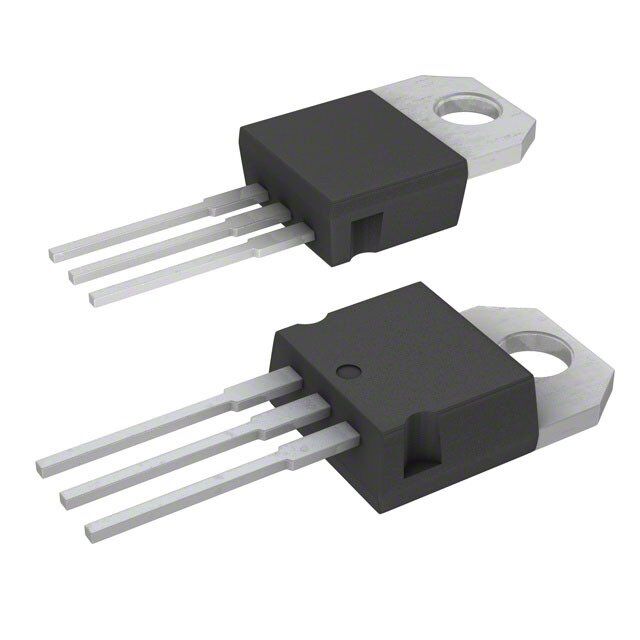
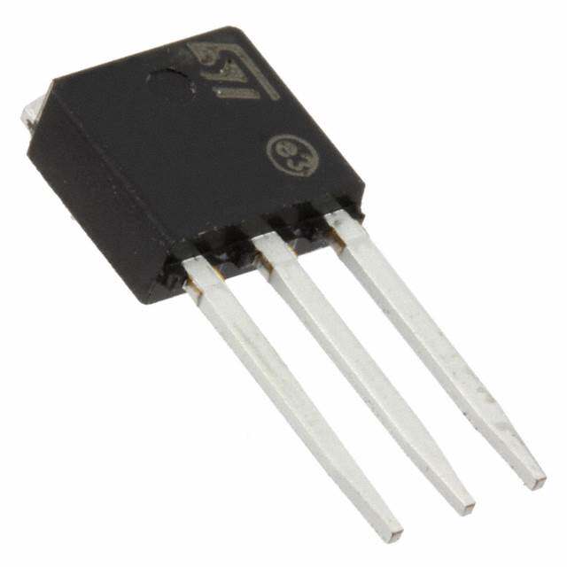
| 产品图片 |
|
| rohs | 符合RoHS无铅 / 符合限制有害物质指令(RoHS)规范要求 |
| 产品系列 | 晶体管,MOSFET,STMicroelectronics STP200NF04STripFET™ II |
| 数据手册 | |
| 产品型号 | STP200NF04 |
| Pd-PowerDissipation | 310 W |
| Pd-功率耗散 | 310 W |
| RdsOn-Drain-SourceResistance | 3.7 mOhms |
| RdsOn-漏源导通电阻 | 3.7 mOhms |
| Vds-Drain-SourceBreakdownVoltage | 40 V |
| Vds-漏源极击穿电压 | 40 V |
| Vgs-Gate-SourceBreakdownVoltage | +/- 20 V |
| Vgs-栅源极击穿电压 | 20 V |
| 上升时间 | 320 ns |
| 下降时间 | 120 ns |
| 不同Id时的Vgs(th)(最大值) | 4V @ 250µA |
| 不同Vds时的输入电容(Ciss) | 5100pF @ 25V |
| 不同Vgs时的栅极电荷(Qg) | 210nC @ 10V |
| 不同 Id、Vgs时的 RdsOn(最大值) | 3.7 毫欧 @ 90A,10V |
| 产品目录页面 | |
| 产品种类 | MOSFET |
| 供应商器件封装 | TO-220AB |
| 其它名称 | 497-3524-5 |
| 其它有关文件 | http://www.st.com/web/catalog/sense_power/FM100/CL824/SC1164/PF69535?referrer=70071840 |
| 典型关闭延迟时间 | 140 ns |
| 功率-最大值 | 310W |
| 包装 | 管件 |
| 单位重量 | 1.438 g |
| 商标 | STMicroelectronics |
| 安装类型 | 通孔 |
| 安装风格 | Through Hole |
| 封装 | Tube |
| 封装/外壳 | TO-220-3 |
| 封装/箱体 | TO-220-3 |
| 工厂包装数量 | 50 |
| 晶体管极性 | N-Channel |
| 最大工作温度 | + 175 C |
| 最小工作温度 | - 55 C |
| 标准包装 | 50 |
| 漏源极电压(Vdss) | 40V |
| 电流-连续漏极(Id)(25°C时) | 120A (Tc) |
| 系列 | STP200NF04 |
| 通道模式 | Enhancement |
| 配置 | Single |


- 商务部:美国ITC正式对集成电路等产品启动337调查
- 曝三星4nm工艺存在良率问题 高通将骁龙8 Gen1或转产台积电
- 太阳诱电将投资9.5亿元在常州建新厂生产MLCC 预计2023年完工
- 英特尔发布欧洲新工厂建设计划 深化IDM 2.0 战略
- 台积电先进制程称霸业界 有大客户加持明年业绩稳了
- 达到5530亿美元!SIA预计今年全球半导体销售额将创下新高
- 英特尔拟将自动驾驶子公司Mobileye上市 估值或超500亿美元
- 三星加码芯片和SET,合并消费电子和移动部门,撤换高东真等 CEO
- 三星电子宣布重大人事变动 还合并消费电子和移动部门
- 海关总署:前11个月进口集成电路产品价值2.52万亿元 增长14.8%


PDF Datasheet 数据手册内容提取
STP200NF04 STB200NF04 - STB200NF04-1 N-CHANNEL 40V - 120A TO-220/D2PAK/I2PAK STripFET™ II POWER MOSFET PRELIMINARYDATA TYPE VDSS RDS(on) ID Pw STP200NF04 40V <0.0037W 120A 310W STB200NF04 40V <0.0037W 120A 310W STB200NF04-1 40V <0.0037W 120A 310W STANDARDTHRESHOLDDRIVE n 3 n 100% AVALANCHE TESTED 12 TO-220 I2PAK DESCRIPTION 3 1 ThisMOSFETisthelatestdevelopmentofSTMicro- electronics unique “Single Feature Size™” strip- D2PAK based process. The resulting transistor shows ex- tremely high packing density for low on-resistance, rugged avalanche characteristics and less critical alignmentstepsthereforearemarkablemanufactur- ingreproducibility. INTERNALSCHEMATICDIAGRAM APPLICATIONS HIGHCURRENT,HIGHSWITCHINGSPEED n AUTOMOTIVE n ORDERINGINFORMATION SALESTYPE MARKING PACKAGE PACKAGING STP200NF04 P200NF04 TO-220 TUBE STB200NF04T4 B200NF04 D2PAK TAPE&REEL STB200NF04-1 B200NF04 I2PAK TUBE December2003 1/13
STP200NF04 - STB200NF04 - STB200NF04-1 ABSOLUTEMAXIMUMRATINGS Symbol Parameter Value Unit VDS Drain-sourceVoltage(VGS=0) 40 V VDGR Drain-gateVoltage(RGS=20kW ) 40 V VGS Gate-sourceVoltage ±20 V ID(#) DrainCurrent(continuos)atTC=25°C 120 A ID(#) DrainCurrent(continuos)atTC=100°C 120 A IDM((cid:1)) DrainCurrent(pulsed) 480 A PTOT TotalDissipationatTC=25°C 310 W DeratingFactor 2.07 W/°C dv/dt(1) PeakDiodeRecoveryvoltageslope 1.5 V/ns EAS(2) SinglePulseAvalancheEnergy 1.3 J Tj OperatingJunctionTemperature -55to175 °C Tstg StorageTemperature (cid:1) ( )Pulsewidthlimitedbysafeoperatingarea (1)ISD£ 120A,di/dt£ 500A/µs,VDD£ V(BR)DSS,Tj£ TJMAX. (2)StartingTj=25°C,Id=60A,VDD=30V (#)CurrentLimitedbyPackage THERMALDATA TO-220/I2PAK/D2PAK Rthj-case ThermalResistanceJunction-caseMax 0.48 °C/W Rthj-pcb ThermalResistanceJunction-pcbMax SeeCurveonpage4 °C/W Rthj-amb ThermalResistanceJunction-ambient(Freeair)Max 62.5 °C/W Tl MaximumLeadTemperatureForSolderingPurpose 300 °C ELECTRICALCHARACTERISTICS (TCASE =25°CUNLESSOTHERWISE SPECIFIED) ON/OFF Symbol Parameter TestConditions Min. Typ. Max. Unit V(BR)DSS Drain-source ID=250µA,VGS=0 40 V BreakdownVoltage IDSS ZeroGateVoltage VDS=MaxRating 1 µA DrainCurrent(VGS=0) VDS=MaxRating,TC=125°C 10 µA IGSS Gate-bodyLeakage VGS=±20V ±100 nA Current(VDS=0) VGS(th) GateThresholdVoltage VDS=VGS,ID=250µA 2 4 V RDS(on) StaticDrain-sourceOn VGS=10V,ID=90A 0.0037 W Resistance 2/13
STP200NF04 - STB200NF04 - STB200NF04-1 ELECTRICALCHARACTERISTICS (CONTINUED) DYNAMIC Symbol Parameter TestConditions Min. Typ. Max. Unit gfs(1) ForwardTransconductance VDS=15V,ID=90A 150 S Ciss InputCapacitance VDS=25V,f=1MHz,VGS=0 5100 pF Coss OutputCapacitance 1600 pF Crss ReverseTransfer 600 pF Capacitance SWITCHINGON Symbol Parameter TestConditions Min. Typ. Max. Unit td(on) Turn-onDelayTime VDD=20V,ID=90A 30 ns tr RiseTime RG=4.7W VGS=10V 320 ns (ResistiveLoadsee,Figure3) Qg TotalGateCharge VDD=20V,ID=120A, 170 210 nC Qgs Gate-SourceCharge VGS=10V 30 nC Qgd Gate-DrainCharge (see,Figure4) 45 nC SWITCHINGOFF Symbol Parameter TestConditions Min. Typ. Max. Unit td(off) Turn-offDelayTime VDD=20V,ID=90A 140 ns tf FallTime RG=4.7W VGS=10V 120 ns (ResistiveLoadsee,Figure3) SOURCEDRAINDIODE Symbol Parameter TestConditions Min. Typ. Max. Unit ISD Source-drainCurrent 120 A ISDM(2) Source-drainCurrent(pulsed) 480 A VSD(1) ForwardOnVoltage ISD=120A,VGS=0 1.3 V trr ReverseRecoveryTime ISD=120A,di/dt=100A/µs 85 ns Qrr ReverseRecoveryCharge VDD=30V,Tj=150°C 190 nC IRRM ReverseRecoveryCurrent (seetestcircuit,Figure5) 4.5 A Note: 1. Pulsed:Pulseduration=300µs,dutycycle1.5%. 2. Pulsewidthlimitedbysafeoperatingarea. 3/13
STP200NF04 - STB200NF04 - STB200NF04-1 ThermalResistanceRthj-avsPCBCopperArea MaxPowerDissipationvsPCBCopperArea 4/13
STP200NF04 - STB200NF04 - STB200NF04-1 AllowableIavvs. TimeinAvalanche Thepreviouscurvegivesthesafeoperatingareaforunclampedinductiveloads,singlepulseorrepetitive, underthefollowingconditions: P =0.5*(1.3*BV *I ) D(AVE) DSS AV EAS(AR)=PD(AVE) *tAV Where: IAV is theAllowableCurrentinAvalanche PD(AVE)istheAveragePowerDissipationinAvalanche(SinglePulse) tAVis theTimeinAvalanche Toderateabove25°C,at fixedIAV,thefollowingequationmustbeapplied: I =2*(T -T )/(1.3*BV *Z ) AV jmax CASE DSS th Where: Z =K *R isthevaluecomingfromNormalizedThermalResponseatfixedpulsewidthequaltoT . th th AV 5/13
STP200NF04 - STB200NF04 - STB200NF04-1 SPICE THERMAL MODEL Parameter Node Value CTHERM1 1-2 1.4958E-3 CTHERM2 2-3 3.5074E-2 CTHERM3 3-4 5.939E-2 CTHERM4 4-5 9.7411E-2 CTHERM5 5-6 8.8596E-2 CTHERM6 6-7 8.2755E-1 RTHERM1 1-2 0.0384 RTHERM2 2-3 0.0624 RTHERM3 3-4 0.072 RTHERM4 4-5 0.0912 RTHERM5 5-6 0.1008 RTHERM6 6-7 0.1152 6/13
STP200NF04 - STB200NF04 - STB200NF04-1 Fig.1:UnclampedInductiveLoadTestCircuit Fig.2:UnclampedInductiveWaveform Fig.3:SwitchingTimes TestCircuitFor Fig.3.1:InductiveLoadSwitchingAndDiodeRe- covery Times Waveform ResistiveLoad Fig.4:GateChargetest Circuit Fig.4.1:GateChargetestWaveform 7/13
STP200NF04 - STB200NF04 - STB200NF04-1 Fig.5:TestCircuitForDiodeRecovery Times Fig.5.1:DiodeRecoveryTimesWaveform 8/13
STP200NF04 - STB200NF04 - STB200NF04-1 TO-220 MECHANICAL DATA mm. inch DIM. MIN. TYP MAX. MIN. TYP. MAX. A 4.40 4.60 0.173 0.181 b 0.61 0.88 0.024 0.034 b1 1.15 1.70 0.045 0.066 c 0.49 0.70 0.019 0.027 D 15.25 15.75 0.60 0.620 E 10 10.40 0.393 0.409 e 2.40 2.70 0.094 0.106 e1 4.95 5.15 0.194 0.202 F 1.23 1.32 0.048 0.052 H1 6.20 6.60 0.244 0.256 J1 2.40 2.72 0.094 0.107 L 13 14 0.511 0.551 L1 3.50 3.93 0.137 0.154 L20 16.40 0.645 L30 28.90 1.137 øP 3.75 3.85 0.147 0.151 Q 2.65 2.95 0.104 0.116 9/13
STP200NF04 - STB200NF04 - STB200NF04-1 D2PAK MECHANICAL DATA mm. inch DIM. MIN. TYP MAX. MIN. TYP. MAX. A 4.4 4.6 0.173 0.181 A1 2.49 2.69 0.098 0.106 A2 0.03 0.23 0.001 0.009 B 0.7 0.93 0.027 0.036 B2 1.14 1.7 0.044 0.067 C 0.45 0.6 0.017 0.023 C2 1.23 1.36 0.048 0.053 D 8.95 9.35 0.352 0.368 D1 8 0.315 E 10 10.4 0.393 E1 8.5 0.334 G 4.88 5.28 0.192 0.208 L 15 15.85 0.590 0.625 L2 1.27 1.4 0.050 0.055 L3 1.4 1.75 0.055 0.068 M 2.4 3.2 0.094 0.126 R 0.4 0.015 V2 0º 8º 3 10/13 1
STP200NF04 - STB200NF04 - STB200NF04-1 TO-262(I2PAK)MECHANICALDATA mm. inch DIM. MIN. TYP MAX. MIN. TYP. MAX. A 4.40 4.60 0.173 0.181 A1 2.40 2.72 0.094 0.107 b 0.61 0.88 0.024 0.034 b1 1.14 1.70 0.044 0.066 c 0.49 0.70 0.019 0.027 c2 1.23 1.32 0.048 0.052 D 8.95 9.35 0.352 0.368 e 2.40 2.70 0.094 0.106 e1 4.95 5.15 0.194 0.202 E 10 10.40 0.393 0.410 L 13 14 0.511 0.551 L1 3.50 3.93 0.137 0.154 L2 1.27 1.40 0.050 0.055 11/13
STP200NF04 - STB200NF04 - STB200NF04-1 2 D PAK FOOTPRINT TUBE SHIPMENT (no suffix)* TAPE AND REEL SHIPMENT (suffix ”T4”)* REEL MECHANICAL DATA mm inch DIM. MIN. MAX. MIN. MAX. A 330 12.992 B 1.5 0.059 C 12.8 13.2 0.504 0.520 D 20.2 0795 G 24.4 26.4 0.960 1.039 N 100 3.937 T 30.4 1.197 BASE QTY BULKQTY TAPE MECHANICAL DATA 1000 1000 mm inch DIM. MIN. MAX. MIN. MAX. A0 10.5 10.7 0.413 0.421 B0 15.7 15.9 0.618 0.626 D 1.5 1.6 0.059 0.063 D1 1.59 1.61 0.062 0.063 E 1.65 1.85 0.065 0.073 F 11.4 11.6 0.449 0.456 K0 4.8 5.0 0.189 0.197 P0 3.9 4.1 0.153 0.161 P1 11.9 12.1 0.468 0.476 P2 1.9 2.1 0.075 0.082 R 50 1.574 T 0.25 0.35 0.0098 0.0137 W 23.7 24.3 0.933 0.956 *onsalestype 12/13
STP200NF04 - STB200NF04 - STB200NF04-1 Information furnished is believed to be accurate and reliable. However, STMicroelectronics assumes no responsibility for the consequences of use of such information nor for any infringement of patents or other rights of third parties which may result from its use. No license is granted by implication or otherwise under any patent or patent rights of STMicroelectronics. Specifications mentioned in this publication are subject to change without notice. This publication supersedes and replaces all information previously supplied. STMicroelectronics products are not authorized for use as critical components in life support devices or systems without express written approval of STMicroelectronics. © The ST logo is a registered trademark of STMicroelectronics © 2003 STMicroelectronics - Printed in Italy - All Rights Reserved STMicroelectronics GROUP OF COMPANIES Australia - Brazil - Canada - China - Finland - France - Germany - Hong Kong - India - Israel - Italy - Japan - Malaysia - Malta - Morocco Singapore - Spain - Sweden - Switzerland - United Kingdom - United States. © http://www.st.com 13/13