ICGOO在线商城 > 分立半导体产品 > 晶体管 - FET,MOSFET - 单 > STD6N95K5

 Datasheet下载
- 型号: STD6N95K5
- 制造商: STMicroelectronics
- 库位|库存: xxxx|xxxx
- 要求:
| 数量阶梯 | 香港交货 | 国内含税 |
| +xxxx | $xxxx | ¥xxxx |
查看当月历史价格
查看今年历史价格
STD6N95K5产品简介:
ICGOO电子元器件商城为您提供STD6N95K5由STMicroelectronics设计生产,在icgoo商城现货销售,并且可以通过原厂、代理商等渠道进行代购。 STD6N95K5价格参考。STMicroelectronicsSTD6N95K5封装/规格:晶体管 - FET,MOSFET - 单, N-Channel 950V 9A (Tc) 90W (Tc) Surface Mount DPAK。您可以下载STD6N95K5参考资料、Datasheet数据手册功能说明书,资料中有STD6N95K5 详细功能的应用电路图电压和使用方法及教程。
STMicroelectronics(意法半导体)的STD6N95K5是一款高压MOSFET,属于晶体管 - FET,MOSFET - 单类别。该器件具有950V的高漏源击穿电压和6A的连续漏极电流能力,适用于高耐压、中等功率的应用场景。

典型应用场景包括:
1. 开关电源(SMPS):广泛用于工业电源、适配器和充电器中,特别是在反激式或正激式拓扑结构中作为主开关元件,具备良好的开关性能和效率。
2. 照明系统:应用于电子镇流器、LED驱动电源等高压照明设备,支持高输入电压环境下的稳定工作。
3. 电机驱动:在小型工业电机控制或家用电器(如空调、洗衣机)的辅助电源和控制电路中提供高效开关功能。
4. 高电压DC-DC转换器:适用于需要将高压直流电转换为低压直流电的工业或电信电源系统。
5. 待机电源与辅助电源电路:因其低静态电流和高耐压特性,适合用于主电源关闭后的待机供电模块。

STD6N95K5采用先进的平面栅极技术,具备优秀的雪崩能量耐受能力和热稳定性,同时内部集成快速恢复体二极管,有助于减少外部元件数量,提高系统可靠性。其TO-220FP或类似封装形式利于散热,适用于紧凑型高功率密度设计。

总体而言,该MOSFET特别适合要求高电压隔离、高可靠性和高能效的工业与消费类电源应用。
| 参数 | 数值 |
| 产品目录 | |
| 描述 | MOSFET N-CH 950V 9A DPAKMOSFET N-Ch 950V 1 Ohm 9A Zener SuperMESH 5 |
| 产品分类 | FET - 单分离式半导体 |
| FET功能 | 标准 |
| FET类型 | MOSFET N 通道,金属氧化物 |
| Id-连续漏极电流 | 9 A |
| 品牌 | STMicroelectronics |
| 产品手册 | |
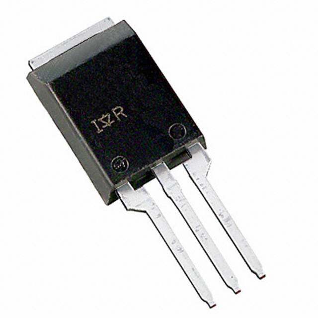
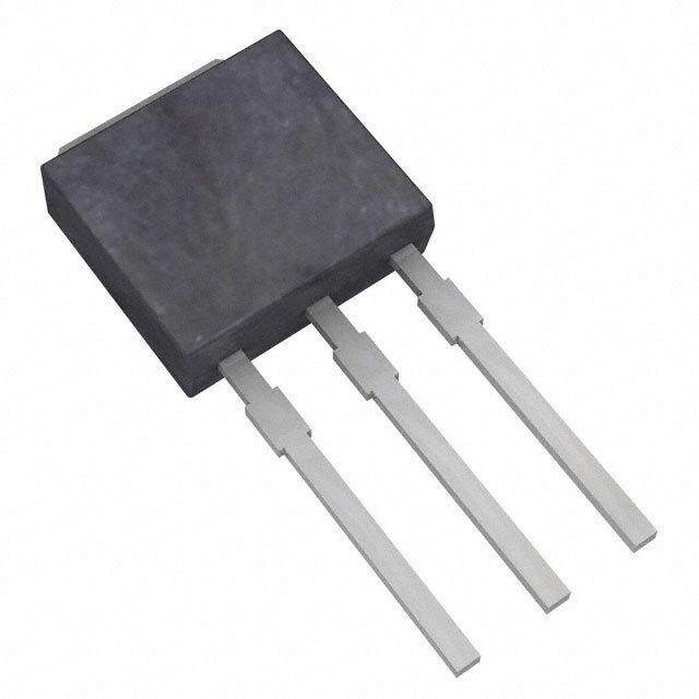
| 产品图片 |
|
| rohs | 符合RoHS无铅 / 符合限制有害物质指令(RoHS)规范要求 |
| 产品系列 | 晶体管,MOSFET,STMicroelectronics STD6N95K5SuperMESH5™ |
| 数据手册 | |
| 产品型号 | STD6N95K5 |
| Pd-PowerDissipation | 90 W |
| Pd-功率耗散 | 90 W |
| Qg-GateCharge | 13 nC |
| Qg-栅极电荷 | 13 nC |
| RdsOn-漏源导通电阻 | 1.25 Ohms |
| Vds-漏源极击穿电压 | 950 V |
| Vgs-Gate-SourceBreakdownVoltage | 30 V |
| Vgs-栅源极击穿电压 | 30 V |
| 不同Id时的Vgs(th)(最大值) | 5V @ 100µA |
| 不同Vds时的输入电容(Ciss) | 450pF @ 100V |
| 不同Vgs时的栅极电荷(Qg) | 13nC @ 10V |
| 不同 Id、Vgs时的 RdsOn(最大值) | 1.25 欧姆 @ 3A,10V |
| 产品种类 | Power MOSFET Transistors |
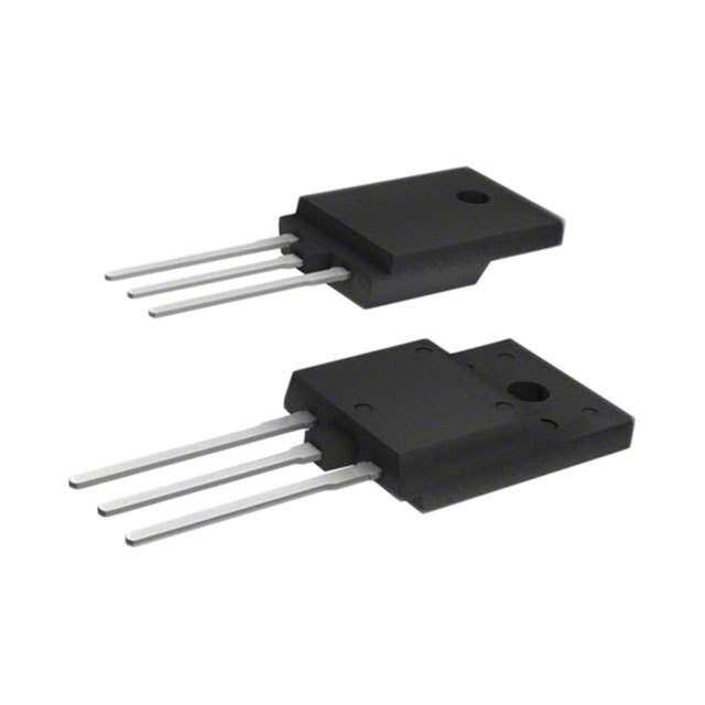
| 供应商器件封装 | D-Pak |
| 其它名称 | 497-12852-1 |
| 其它有关文件 | http://www.st.com/web/catalog/sense_power/FM100/CL824/SC1168/PF248786?referrer=70071840 |
| 功率-最大值 | 90W |
| 包装 | 剪切带 (CT) |
| 商标 | STMicroelectronics |
| 安装类型 | 表面贴装 |
| 安装风格 | SMD/SMT |
| 导通电阻 | 1.25 Ohms |
| 封装 | Reel |
| 封装/外壳 | TO-252-3,DPak(2 引线+接片),SC-63 |
| 封装/箱体 | DPAK |
| 工厂包装数量 | 2500 |
| 晶体管极性 | N-Channel |
| 最大工作温度 | + 150 C |
| 最小工作温度 | - 55 C |
| 标准包装 | 1 |
| 汲极/源极击穿电压 | 950 V |
| 漏极连续电流 | 9 A |
| 漏源极电压(Vdss) | 950V |
| 电流-连续漏极(Id)(25°C时) | 9A (Tc) |
| 系列 | STD6N95K5 |


- 商务部:美国ITC正式对集成电路等产品启动337调查
- 曝三星4nm工艺存在良率问题 高通将骁龙8 Gen1或转产台积电
- 太阳诱电将投资9.5亿元在常州建新厂生产MLCC 预计2023年完工
- 英特尔发布欧洲新工厂建设计划 深化IDM 2.0 战略
- 台积电先进制程称霸业界 有大客户加持明年业绩稳了
- 达到5530亿美元!SIA预计今年全球半导体销售额将创下新高
- 英特尔拟将自动驾驶子公司Mobileye上市 估值或超500亿美元
- 三星加码芯片和SET,合并消费电子和移动部门,撤换高东真等 CEO
- 三星电子宣布重大人事变动 还合并消费电子和移动部门
- 海关总署:前11个月进口集成电路产品价值2.52万亿元 增长14.8%


PDF Datasheet 数据手册内容提取
STD6N95K5, STP6N95K5 STU6N95K5, STW6N95K5 Datasheet N-channel 950 V, 1 Ω typ., 9 A MDmesh™ K5 Power MOSFETs in DPAK, TO-220, IPAK and TO-247 packages Features TAB TAB Order codes VDS RDS(on) max. ID PTOT 3 DPAK 1 STD6N95K5 TO-220 3 STP6N95K5 2 1 950 V 1.25 Ω 9 A 90 W TAB STU6N95K5 STW6N95K5 • DPAK 950 V worldwide best R DS(on) 3 IPAK 12 3 • Worldwide best FOM (figure of merit) 2 TO-247 1 • Ultra low gate charge • 100% avalanche tested D(2, TAB) • Zener-protected Applications G(1) • Switching applications Description S(3) AM01475V1 These very high voltage N-channel Power MOSFETs are designed using MDmesh™ K5 technology based on an innovative proprietary vertical structure. The result is a dramatic reduction in on-resistance and ultra-low gate charge for applications Product status link requiring superior power density and high efficiency. STD6N95K5 STP6N95K5 STU6N95K5 STW6N95K5 DS6666 - Rev 5 - March 2018 www.st.com For further information contact your local STMicroelectronics sales office.
STD6N95K5, STP6N95K5, STU6N95K5, STW6N95K5 Electrical ratings 1 Electrical ratings Table 1. Absolute maximum ratings Symbol Parameter Value Unit VGS Gate- source voltage ± 30 V ID Drain current (continuous) at TC = 25 °C 9 A ID Drain current (continuous) at TC = 100 °C 6 A IDM (1) Drain current (pulsed) 24 A PTOT Total dissipation at TC = 25 °C 90 W IAR (2) Max current during repetitive or single pulse avalanche 3 A Single pulse avalanche energy EAS 90 mJ (starting TJ = 25 °C, ID=IAS, VDD= 50 V) dv/dt (3) Peak diode recovery voltage slope 4.5 V/ns dv/dt (4) MOSFET dv/dt ruggedness 50 V/ns Tj Operating junction temperature range - 55 to 150 °C Tstg Storage temperature range 1. Pulse width limited by safe operating area. 2. Pulse width limited by TJmax. 3. ISD ≤ 9 A, di/dt ≤ 100 A/µs, VDS(peak) ≤ V(BR)DSS 4. VDS ≤ 760 V Table 2. Thermal data Value Symbol Parameter TO-220, Unit DPAK TO-247 IPAK Rthj-case Thermal resistance junction-case 1.39 °C/W Rthj-amb Thermal resistance junction-amb 62.5 50 °C/W Rthj-pcb (1) Thermal resistance junction-pcb 50 °C/W 1. When mounted on 1 inch² FR-4 board, 2 oz Cu DS6666 - Rev 5 page 2/26
STD6N95K5, STP6N95K5, STU6N95K5, STW6N95K5 Electrical characteristics 2 Electrical characteristics (T = 25 °C unless otherwise specified) CASE Table 3. On/off states Symbol Parameter Test conditions Min. Typ. Max. Unit Drain-source breakdown V(BR)DSS voltage VGS= 0 V, ID = 1 mA 950 V Zero gate voltage drain VGS = 0 V, VDS = 950 V 1 µA IDSS current VGS = 0 V, VDS = 950 V, Tc=125 °C(1) 50 µA IGSS Gate body leakage current VDS = 0, VGS = ± 20 V ±10 µA VGS(th) Gate threshold voltage VDS = VGS, ID = 100 µA 3 4 5 V Static drain-source on- RDS(on) resistance VGS = 10 V, ID= 3 A 1 1.25 Ω 1. Defined by design, not subject to production test. Table 4. Dynamic Symbol Parameter Test conditions Min. Typ. Max. Unit Ciss Input capacitance - 450 - pF Coss Output capacitance VGS=0 V, VDS =100 V, f=1 MHz - 30 - pF Crss Reverse transfer capacitance - 1.6 - pF Equivalent capacitance time Co(tr) (1) related - 45 - pF VGS = 0 V, VDS = 0 to 760 V Equivalent capacitance Co(er) (2) energy related - 19 - pF RG Intrinsic gate resistance f = 1 MHz, ID=0 A - 7 - Ω Qg Total gate charge - 13 - nC VDD = 760 V, ID = 6 A, Qgs Gate-source charge VGS = 0 to 10 V, (see Figure 17. Test - 3 - nC circuit for gate charge behavior) Qgd Gate-drain charge - 7 - nC 1. Co(tr) is a constant capacitance value that gives the same charging time as Coss while VDS is rising from 0 to 80% VDSS. 2. Co(er) is a constant capacitance value that gives the same stored energy as Coss while VDS is rising from 0 to 80% VDSS. Table 5. Switching times Symbol Parameter Test conditions Min. Typ. Max. Unit td(on) Turn-on delay time VDD = 475 V, ID = 3 A, RG=4.7 Ω, - 12 - ns tr Rise time VGS=10 V - 12 - ns (see Figure 16. Test circuit for td(off) Turn-off delay time resistive load switching times and - 33 - ns tf Fall time Figure 21. Switching time waveform) - 21 - ns DS6666 - Rev 5 page 3/26
STD6N95K5, STP6N95K5, STU6N95K5, STW6N95K5 Electrical characteristics Table 6. Source drain diode Symbol Parameter Test conditions Min. Typ. Max. Unit ISD Source-drain current - 9 A ISDM(1) Source-drain current (pulsed) - 24 A VSD (2) Forward on voltage ISD= 6 A, VGS=0 V - 1.6 V trr Reverse recovery time ISD= 6 A, VDD= 60 V - 372 ns Qrr Reverse recovery charge di/dt = 100 A/µs, - 4 µC (see Figure 18. Test circuit for IRRM Reverse recovery current inductive load switching and diode - 22 A recovery times) trr Reverse recovery time ISD= 6 A,VDD= 60 V - 522 ns Qrr Reverse recovery charge di/dt=100 A/µs, Tj=150 °C - 5 µC (see Figure 18. Test circuit for IRRM Reverse recovery current inductive load switching and diode - 20 A recovery times) 1. Pulse width limited by safe operating area. 2. Pulsed: pulse duration = 300µs, duty cycle 1.5% Table 7. Gate-source Zener diode Symbol Parameter Test conditions Min Typ. Max. Unit Gate-source breakdown V(BR)GSO voltage IGS = ± 1mA, ID= 0 A ±30 - - V The built-in back-to-back Zener diodes are specifically designed to enhance the ESD performance of the device. The Zener voltage facilitates efficient and cost-effective device integrity protection, thus eliminating the need for additional external componentry. DS6666 - Rev 5 page 4/26
STD6N95K5, STP6N95K5, STU6N95K5, STW6N95K5 Electrical characteristics (curves) 2.1 Electrical characteristics (curves) Figure 1. Safe operating area for DPAK and IPAK Figure 2. Thermal impedance for DPAK and IPAK ID AM07105v1 K GC20460 (A) Tj=150°C Tc=25°C Single pulse 10 10µs 1 Operatmiitoen di nb ty hims aaxr eRa DiSs( on) 110m0sµ s 100 Li 10ms 10-1 0.1 0.01 10-2 0.1 1 10 100 VDS(V) 10-5 10-4 10-3 10-2 10-1 tp (s) Figure 3. Safe operating area for TO-220 and TO-247 Figure 4. Thermal impedance for TO-220 and TO-247 ID AM07107v1 (A) Tj=150°C Tc=25°C Single pulse 101 Operatmiitoen di nb ty hims aaxr eRa DiSs( on) 11100m0µsµs s Li 10ms 0.1 0.01 0.1 1 10 100 VDS(V) Figure 5. Output characteristics Figure 6. Transfer characteristics ID(A) AM07108v1 ID AM07109v1 (A) VGS=10V VDS=15V 12 8 10 6 8 7V 6 4 4 6V 2 2 5V 0 0 0 5 10 15 20 25 VDS(V) 0 2 4 6 8 VGS(V) DS6666 - Rev 5 page 5/26
STD6N95K5, STP6N95K5, STU6N95K5, STW6N95K5 Electrical characteristics (curves) Figure 7. Gate charge vs gate-source voltage Figure 8. Static drain-source on-resistance VGS AMV0D71S10v1 RDS(on) AM07111v1 (V) (Ohm) (V) VDS VDD=760V 700 1.03 VGS=10V 12 ID=6A 1.01 600 10 0.99 500 8 0.97 400 0.95 6 300 0.93 4 200 0.91 2 100 0.89 0 0 0.87 0 2 4 6 8 10 12 14 Qg(nC) 0.5 1.0 1.5 2.0 2.5 3.0 ID(A) Figure 9. Capacitance variations Figure 10. Output capacitance storage energy C AM07112v1 Eoss (µJ) AM07113v1 (pF) 22 20 1000 11 8 Ciss 16 14 100 12 10 f = 1 MHz Coss 8 10 6 Crss 4 2 1 0.1 1 10 100 VDS(V) 00 100 200 300 400 500 600 700 800 900 VDS(V) Figure 11. Normalized gate threshold voltage vs Figure 12. Normalized on-resistance vs temperature temperature RDS(on) AM07115v1 VG(nSo(rtmh)) AM07114v1 (norm) VGS=10V 1.2 ID=100µA 2.5 ID=3A 1.1 2.0 1.0 1.5 0.9 0.8 1.0 0.7 0.6 0.5 0.5 0 0.4 -75 -25 25 75 125 TJ(°C) -75 -25 25 75 125 TJ(°C) DS6666 - Rev 5 page 6/26
STD6N95K5, STP6N95K5, STU6N95K5, STW6N95K5 Electrical characteristics (curves) Figure 13. Source-drain diode forward characteristics Figure 14. Normalized V vs temperature (BR)DSS VSD AM07118v1 V(BR)DSS AM07116v1 (V) (norm) ID=1 mA 0.95 TJ=-50°C 1.2 1.1 0.85 TJ=25°C 1.0 0.75 0.9 0.65 TJ=150°C 0.8 0.7 0.55 2.0 3.0 4.0 5.0 6.0 ISD(A) -75 -25 25 75 125 TJ(°C) Figure 15. Maximum avalanche energy vs starting T j AM07117v1 EAS(mJ) 100 ID=3 A 90 VDD=50 V 80 70 60 50 40 30 20 10 0 0 20 40 60 80 100 120 140 TJ(°C) DS6666 - Rev 5 page 7/26
STD6N95K5, STP6N95K5, STU6N95K5, STW6N95K5 Test circuits 3 Test circuits Figure 16. Test circuit for resistive load switching times Figure 17. Test circuit for gate charge behavior VDD 12 V 47 kΩ 1 kΩ 100 nF RL 2200 3.3 + μF μF VDD VD VGS IG= CONST 100 Ω D.U.T. VGS RG D.U.T. pulse width 2200+ 2.7 kΩ VG pulse width μF 47 kΩ 1 kΩ AM01468v1 AM01469v1 Figure 18. Test circuit for inductive load switching and Figure 19. Unclamped inductive load test circuit diode recovery times L D A A A VD G D.U.T. fdaiostde 100 µH +2µ2F00 3µ.F3 VDD 25 Ω S B B B D µ3F.3 +1µ0F00 VDD ID G D.U.T. + RG S Vi D.U.T. _ pulse width AM01471v1 AM01470v1 Figure 20. Unclamped inductive waveform Figure 21. Switching time waveform V(BR)DSS VD ton toff td(on) tr td(off) tf IDM 90% 90% 10% ID 0 10% VDS VDD VDD VGS 90% 0 10% AM01472v1 AM01473v1 DS6666 - Rev 5 page 8/26
STD6N95K5, STP6N95K5, STU6N95K5, STW6N95K5 Package information 4 Package information In order to meet environmental requirements, ST offers these devices in different grades of ECOPACK® packages, depending on their level of environmental compliance. ECOPACK® specifications, grade definitions and product status are available at: www.st.com. ECOPACK® is an ST trademark. DS6666 - Rev 5 page 9/26
STD6N95K5, STP6N95K5, STU6N95K5, STW6N95K5 DPAK (TO-252) type A2 package information 4.1 DPAK (TO-252) type A2 package information Figure 22. DPAK (TO-252) type A2 package outline 0068772_type-A2_rev24 DS6666 - Rev 5 page 10/26
STD6N95K5, STP6N95K5, STU6N95K5, STW6N95K5 DPAK (TO-252) type A2 package information Table 8. DPAK (TO-252) type A2 mechanical data mm Dim. Min. Typ. Max. A 2.20 2.40 A1 0.90 1.10 A2 0.03 0.23 b 0.64 0.90 b4 5.20 5.40 c 0.45 0.60 c2 0.48 0.60 D 6.00 6.20 D1 4.95 5.10 5.25 E 6.40 6.60 E1 5.10 5.20 5.30 e 2.16 2.28 2.40 e1 4.40 4.60 H 9.35 10.10 L 1.00 1.50 L1 2.60 2.80 3.00 L2 0.65 0.80 0.95 L4 0.60 1.00 R 0.20 V2 0° 8° DS6666 - Rev 5 page 11/26
STD6N95K5, STP6N95K5, STU6N95K5, STW6N95K5 DPAK (TO-252) type C2 package information 4.2 DPAK (TO-252) type C2 package information Figure 23. DPAK (TO-252) type C2 package outline 0068772_C2_24 DS6666 - Rev 5 page 12/26
STD6N95K5, STP6N95K5, STU6N95K5, STW6N95K5 DPAK (TO-252) type C2 package information Table 9. DPAK (TO-252) type C2 mechanical data mm Dim. Min. Typ. Max. A 2.20 2.30 2.38 A1 0.90 1.01 1.10 A2 0.00 0.10 b 0.72 0.85 b4 5.13 5.33 5.46 c 0.47 0.60 c2 0.47 0.60 D 6.00 6.10 6.20 D1 5.10 5.60 E 6.50 6.60 6.70 E1 5.20 5.50 e 2.186 2.286 2.386 H 9.80 10.10 10.40 L 1.40 1.50 1.70 L1 2.90 REF L2 0.90 1.25 L3 0.51 BSC L4 0.60 0.80 1.00 L6 1.80 BSC θ1 5° 7° 9° θ2 5° 7° 9° V2 0° 8° DS6666 - Rev 5 page 13/26
STD6N95K5, STP6N95K5, STU6N95K5, STW6N95K5 DPAK (TO-252) type C2 package information Figure 24. DPAK (TO-252) recommended footprint (dimensions are in mm) FP_0068772_24 DS6666 - Rev 5 page 14/26
STD6N95K5, STP6N95K5, STU6N95K5, STW6N95K5 DPAK (TO-252) packing information 4.3 DPAK (TO-252) packing information Figure 25. DPAK (TO-252) tape outline 10 pitches cumulative tolerance on tape +/- 0.2 mm Top cover P0 D P2 T tape E F K0 W B1 B0 For machine ref. only A0 P1 D1 including draft and radii concentric around B0 User direction of feed R Bending radius User direction of feed AM08852v1 DS6666 - Rev 5 page 15/26
STD6N95K5, STP6N95K5, STU6N95K5, STW6N95K5 DPAK (TO-252) packing information Figure 26. DPAK (TO-252) reel outline T 40mm min. access hole at slot location B D C N A Tape slot G measured in core for at hub Full radius tape start 2.5mm min.width AM06038v1 Table 10. DPAK (TO-252) tape and reel mechanical data Tape Reel mm mm Dim. Dim. Min. Max. Min. Max. A0 6.8 7 A 330 B0 10.4 10.6 B 1.5 B1 12.1 C 12.8 13.2 D 1.5 1.6 D 20.2 D1 1.5 G 16.4 18.4 E 1.65 1.85 N 50 F 7.4 7.6 T 22.4 K0 2.55 2.75 P0 3.9 4.1 Base qty. 2500 P1 7.9 8.1 Bulk qty. 2500 P2 1.9 2.1 R 40 T 0.25 0.35 W 15.7 16.3 DS6666 - Rev 5 page 16/26
STD6N95K5, STP6N95K5, STU6N95K5, STW6N95K5 TO-220 type A package information 4.4 TO-220 type A package information Figure 27. TO-220 type A package outline 0015988_typeA_Rev_21 DS6666 - Rev 5 page 17/26
STD6N95K5, STP6N95K5, STU6N95K5, STW6N95K5 TO-220 type A package information Table 11. TO-220 type A package mechanical data mm Dim. Min. Typ. Max. A 4.40 4.60 b 0.61 0.88 b1 1.14 1.55 c 0.48 0.70 D 15.25 15.75 D1 1.27 E 10.00 10.40 e 2.40 2.70 e1 4.95 5.15 F 1.23 1.32 H1 6.20 6.60 J1 2.40 2.72 L 13.00 14.00 L1 3.50 3.93 L20 16.40 L30 28.90 øP 3.75 3.85 Q 2.65 2.95 DS6666 - Rev 5 page 18/26
STD6N95K5, STP6N95K5, STU6N95K5, STW6N95K5 IPAK (TO-251) type A package information 4.5 IPAK (TO-251) type A package information Figure 28. IPAK (TO-251) type A package outline 0068771_IK_typeA_rev14 DS6666 - Rev 5 page 19/26
STD6N95K5, STP6N95K5, STU6N95K5, STW6N95K5 IPAK (TO-251) type A package information Table 12. IPAK (TO-251) type A package mechanical data mm Dim. Min. Typ. Max. A 2.20 2.40 A1 0.90 1.10 b 0.64 0.90 b2 0.95 b4 5.20 5.40 B5 0.30 c 0.45 0.60 c2 0.48 0.60 D 6.00 6.20 E 6.40 6.60 e 2.28 e1 4.40 4.60 H 16.10 L 9.00 9.40 L1 0.80 1.20 L2 0.80 1.00 V1 10° DS6666 - Rev 5 page 20/26
STD6N95K5, STP6N95K5, STU6N95K5, STW6N95K5 TO-247 package information 4.6 TO-247 package information Figure 29. TO-247 package outline 0075325_9 DS6666 - Rev 5 page 21/26
STD6N95K5, STP6N95K5, STU6N95K5, STW6N95K5 TO-247 package information Table 13. TO-247 package mechanical data mm Dim. Min. Typ. Max. A 4.85 5.15 A1 2.20 2.60 b 1.0 1.40 b1 2.0 2.40 b2 3.0 3.40 c 0.40 0.80 D 19.85 20.15 E 15.45 15.75 e 5.30 5.45 5.60 L 14.20 14.80 L1 3.70 4.30 L2 18.50 ØP 3.55 3.65 ØR 4.50 5.50 S 5.30 5.50 5.70 DS6666 - Rev 5 page 22/26
STD6N95K5, STP6N95K5, STU6N95K5, STW6N95K5 Ordering information 5 Ordering information Table 14. Ordering information Order code Marking Package Packing STD6N95K5 6N95K5 DPAK Tape and reel STP6N95K5 6N95K5 TO-220 Tube STU6N95K5 6N95K5 IPAK Tube STW6N95K5 6N95K5 TO-247 Tube DS6666 - Rev 5 page 23/26
STD6N95K5, STP6N95K5, STU6N95K5, STW6N95K5 Revision history Table 15. Document revision history Date Revision Changes 12-Jan-2010 1 First release. 01-Jul-2010 2 Document status promoted from preliminary data to datasheet. Inserted new device in IPAK. Updated Table 1: Device summary, Table 2: Absolute maximum ratings, and Table 3: Thermal data. 31-Aug-2012 3 Updated Section 4: Package mechanical data and Section 5: Packaging mechanical data. Minor text changes in the cover page. The part number STF6N95K5 has been moved to a separate datasheet. Added: MOSFET dv/dt ruggedness parameter in Table 2 16-May-2014 4 Updated: Section 4: Package mechanical data Minor text changes Removed maturity status indication and updated title and description from cover page. The document status is production data. Updated Section 1 Electrical ratings, Section 2 Electrical characteristics. 22-Mar-2018 5 Updated Figure 9. Capacitance variations and Figure 12. Normalized on-resistance vs temperature. Updated Section 4 Package information. Minor text changes. DS6666 - Rev 5 page 24/26
STD6N95K5, STP6N95K5, STU6N95K5, STW6N95K5 Contents Contents 1 Electrical ratings...................................................................2 2 Electrical characteristics...........................................................3 2.1 Electrical characteristics (curves).................................................5 3 Test circuits .......................................................................8 4 Package information...............................................................9 4.1 DPAK (TO-252) type A2 package information .....................................10 4.2 DPAK (TO-252) type C2 package information .....................................12 4.3 DPAK (TO-252) packing information .............................................15 4.4 TO-220 type A package information .............................................17 4.5 IPAK (TO-251) type A package information .......................................19 4.6 TO-247 package information ...................................................21 5 Ordering information .............................................................23 Revision history .......................................................................24 DS6666 - Rev 5 page 25/26
STD6N95K5, STP6N95K5, STU6N95K5, STW6N95K5 IMPORTANT NOTICE – PLEASE READ CAREFULLY STMicroelectronics NV and its subsidiaries (“ST”) reserve the right to make changes, corrections, enhancements, modifications, and improvements to ST products and/or to this document at any time without notice. Purchasers should obtain the latest relevant information on ST products before placing orders. ST products are sold pursuant to ST’s terms and conditions of sale in place at the time of order acknowledgement. Purchasers are solely responsible for the choice, selection, and use of ST products and ST assumes no liability for application assistance or the design of Purchasers’ products. No license, express or implied, to any intellectual property right is granted by ST herein. Resale of ST products with provisions different from the information set forth herein shall void any warranty granted by ST for such product. ST and the ST logo are trademarks of ST. All other product or service names are the property of their respective owners. Information in this document supersedes and replaces information previously supplied in any prior versions of this document. © 2018 STMicroelectronics – All rights reserved DS6666 - Rev 5 page 26/26
Mouser Electronics Authorized Distributor Click to View Pricing, Inventory, Delivery & Lifecycle Information: S TMicroelectronics: STD6N95K5 STP6N95K5 STW6N95K5 STU6N95K5