ICGOO在线商城 > 分立半导体产品 > 晶体管 - FET,MOSFET - 单 > STD5N20LT4
 Datasheet下载
- 型号: STD5N20LT4
- 制造商: STMicroelectronics
- 库位|库存: xxxx|xxxx
- 要求:
| 数量阶梯 | 香港交货 | 国内含税 |
| +xxxx | $xxxx | ¥xxxx |
查看当月历史价格
查看今年历史价格
STD5N20LT4产品简介:
ICGOO电子元器件商城为您提供STD5N20LT4由STMicroelectronics设计生产,在icgoo商城现货销售,并且可以通过原厂、代理商等渠道进行代购。 STD5N20LT4价格参考。STMicroelectronicsSTD5N20LT4封装/规格:晶体管 - FET,MOSFET - 单, 表面贴装 N 沟道 200V 5A(Tc) 33W(Tc) DPAK。您可以下载STD5N20LT4参考资料、Datasheet数据手册功能说明书,资料中有STD5N20LT4 详细功能的应用电路图电压和使用方法及教程。
STD5N20LT4 是由 STMicroelectronics(意法半导体)生产的一款 N 沟道增强型功率 MOSFET,属于晶体管 - FET、MOSFET - 单类别的产品。其主要应用场景包括:

1. 开关电源(SMPS)
   STD5N20LT4 的高电压耐受能力(VDS = 200V)使其非常适合用于开关电源中的高频开关应用。它可以作为主开关管或同步整流管,用于降压、升压或反激式转换器中。

2. 电机驱动
   该 MOSFET 可用于小型直流电机的驱动电路中,特别是在需要高电压和低导通电阻(RDS(on) = 0.75Ω @ VGS=10V)的应用场景下。例如,家用电器、玩具、电动工具等领域的电机控制。

3. 负载开关
   在需要快速切换负载的场合,如汽车电子、工业自动化设备中,STD5N20LT4 可以用作负载开关,提供高效的电流控制和保护功能。

4. 逆变器和变频器
   由于其较高的电压和电流处理能力(ID = 5A),STD5N20LT4 可应用于小型逆变器或变频器中,用于交流信号的生成和频率调节。

5. 保护电路
   在过流保护、短路保护或限流电路中,该 MOSFET 可以充当电子开关或限流元件,确保系统在异常情况下安全运行。

6. 音频放大器
   在某些功率音频放大器设计中,STD5N20LT4 可用于输出级,提供稳定的电流输出和良好的线性特性。

7. 电池管理
   适用于电池充电和放电管理电路,尤其是在需要高效率和低功耗的便携式设备中,如锂电池保护板。

8. 照明控制
   用于 LED 照明驱动电路中,实现调光、恒流控制等功能,特别适合高压 LED 应用。

总结来说,STD5N20LT4 凭借其高电压、低导通电阻和优秀的电气性能,广泛应用于电源管理、电机控制、保护电路以及各种工业和消费电子领域。
| 参数 | 数值 |
| 产品目录 | |
| ChannelMode | Enhancement |
| 描述 | MOSFET N-CH 200V 5A DPAKMOSFET N-Ch 200 Volt 5 Amp |
| 产品分类 | FET - 单分离式半导体 |
| FET功能 | 逻辑电平门 |
| FET类型 | MOSFET N 通道,金属氧化物 |
| Id-ContinuousDrainCurrent | 5 A |
| Id-连续漏极电流 | 5 A |
| 品牌 | STMicroelectronics |
| 产品手册 | |
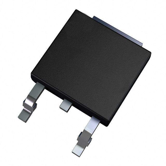
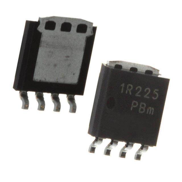
| 产品图片 |
|
| rohs | 符合RoHS无铅 / 符合限制有害物质指令(RoHS)规范要求 |
| 产品系列 | 晶体管,MOSFET,STMicroelectronics STD5N20LT4STripFET™ |
| 数据手册 | |
| 产品型号 | STD5N20LT4 |
| Pd-PowerDissipation | 33 W |
| Pd-功率耗散 | 33 W |
| RdsOn-Drain-SourceResistance | 650 mOhms |
| RdsOn-漏源导通电阻 | 650 mOhms |
| Vds-Drain-SourceBreakdownVoltage | 200 V |
| Vds-漏源极击穿电压 | 200 V |
| Vgs-Gate-SourceBreakdownVoltage | +/- 20 V |
| Vgs-栅源极击穿电压 | 20 V |
| 上升时间 | 21.5 ns |
| 下降时间 | 15.5 ns |
| 不同Id时的Vgs(th)(最大值) | 2.5V @ 50µA |
| 不同Vds时的输入电容(Ciss) | 242pF @ 25V |
| 不同Vgs时的栅极电荷(Qg) | 6nC @ 5V |
| 不同 Id、Vgs时的 RdsOn(最大值) | 700 毫欧 @ 2.5A,5V |
| 产品目录页面 | |
| 产品种类 | MOSFET |
| 供应商器件封装 | D-Pak |
| 其它名称 | 497-4335-1 |
| 其它有关文件 | http://www.st.com/web/catalog/sense_power/FM100/CL824/SC1166/PF82154?referrer=70071840 |
| 典型关闭延迟时间 | 14 ns |
| 功率-最大值 | 33W |
| 包装 | 剪切带 (CT) |
| 商标 | STMicroelectronics |
| 安装类型 | 表面贴装 |
| 安装风格 | SMD/SMT |
| 封装 | Reel |
| 封装/外壳 | TO-252-3,DPak(2 引线+接片),SC-63 |
| 封装/箱体 | DPAK-2 |
| 工厂包装数量 | 2500 |
| 晶体管极性 | N-Channel |
| 最大工作温度 | + 150 C |
| 最小工作温度 | - 55 C |
| 标准包装 | 1 |
| 正向跨导-最小值 | 6.5 S |
| 漏源极电压(Vdss) | 200V |
| 电流-连续漏极(Id)(25°C时) | 5A (Tc) |
| 系列 | STD5N20L |
| 通道模式 | Enhancement |
| 配置 | Single |


- 商务部:美国ITC正式对集成电路等产品启动337调查
- 曝三星4nm工艺存在良率问题 高通将骁龙8 Gen1或转产台积电
- 太阳诱电将投资9.5亿元在常州建新厂生产MLCC 预计2023年完工
- 英特尔发布欧洲新工厂建设计划 深化IDM 2.0 战略
- 台积电先进制程称霸业界 有大客户加持明年业绩稳了
- 达到5530亿美元!SIA预计今年全球半导体销售额将创下新高
- 英特尔拟将自动驾驶子公司Mobileye上市 估值或超500亿美元
- 三星加码芯片和SET,合并消费电子和移动部门,撤换高东真等 CEO
- 三星电子宣布重大人事变动 还合并消费电子和移动部门
- 海关总署:前11个月进口集成电路产品价值2.52万亿元 增长14.8%


PDF Datasheet 数据手册内容提取
STD5N20L Ω N-CHANNEL 200V - 0.65 - 5A DPAK STripFET™ MOSFET Table 1: General Features Figure 1: Package TYPE VDSS RDS(on) ID Pw STD5N20L 200 V < 0.7 Ω 5 A 33 W (cid:1) TYPICAL RDS(on) = 0.65 Ω @ 5V (cid:1) CONDUCTION LOSSES REDUCED (cid:1) LOW INPUT CAPACIATNCE (cid:1) LOW THRESHOLD DEVICE 3 DESCRIPTION 1 The STD5N20L utilizes the latest advanced de- sign rules of ST’s proprietary STripFET™ technol- DPAK ogy. This is suitable for the most demanding DC Motor Control and lighting application. Figure 2: Internal Schematic Diagram APPLICATIONS (cid:1) UPS AND MOTOR CONTROL (cid:1) LIGHTING Table 2: Order Codes SALES TYPE MARKING PACKAGE PACKAGING STD5N20LT4 D5N20L DPAK TAPE & REEL Rev. 3 September 2004 1/10 NEW DATASHEET ACCORDING TO PCN DSG-TRA/04/532
STD5N20L Table 3: Absolute Maximum ratings Symbol Parameter Value Unit VDS Drain-source Voltage (VGS = 0) 200 V VDGR Drain-gate Voltage (RGS = 20 kΩ) 200 V VGS Gate- source Voltage ±20 V ID Drain Current (continuous) at TC = 25°C 5 A ID Drain Current (continuous) at TC = 100°C 3.6 A IDM ((cid:1)) Drain Current (pulsed) 20 A PTOT Total Dissipation at TC = 25°C 33 W Derating Factor 0.27 W/°C Tstg Storage Temperature –55 to 150 °C Tj Operating Junction Temperature ((cid:1)) Pulse width limited by safe operating area Table 4: Thermal Data Rthj-case Thermal Resistance Junction-case Max 3.75 °C/W Rthj-amb Thermal Resistance Junction-ambient Max 100 °C/W Tl Maximum Lead Temperature For Soldering Purpose 275 °C ELECTRICAL CHARACTERISTICS (TCASE =25°C UNLESS OTHERWISE SPECIFIED) Table 5: On/Off Symbol Parameter Test Conditions Min. Typ. Max. Unit V(BR)DSS Drain-source ID = 250 µA, VGS = 0 200 V Breakdown Voltage IDSS Zero Gate Voltage VDS = Max Rating 1 µA Drain Current (VGS = 0) VDS= Max Rating, TC= 125°C 10 µA IGSS Gate-body Leakage VGS = ±20V ±100 nA Current (VDS = 0) VGS(th) Gate Threshold Voltage VDS = VGS, ID = 50µA 1 2.5 V RDS(on) Static Drain-source On VGS = 5 V, ID = 2.5 A 0.65 0.7 Ω Resistance 2/10
STD5N20L Table 6: Dynamic Symbol Parameter Test Conditions Min. Typ. Max. Unit gfs (2) Forward Transconductance VDS = 15 V, ID = 5 A 6.5 S Ciss Input Capacitance VDS = 25V, f = 1 MHz, VGS = 0 242 pF Coss Output Capacitance 44 pF Crss Reverse Transfer 6 pF Capacitance td(on) Turn-on Delay Time VDD = 100 V, ID = 2.5 A 11.5 ns tr Rise Time RG = 4.7Ω, VGS = 5V 21.5 ns td(off) Turn-off Delay Time (Resistive Load see Figure 14) 14 ns tf Fall Time 15.5 ns Qg Total Gate Charge VDD = 160 V, ID = 5 A, 5 6 nC Qgs Gate-Source Charge VGS = 5V 1.5 nC Qgd Gate-Drain Charge 3 nC Table 7: Source Drain Diode Symbol Parameter Test Conditions Min. Typ. Max. Unit ISD Source-drain Current 5 A ISDM (*) Source-drain Current (pulsed) 20 A VSD (1) Forward On Voltage ISD = 5 A, VGS = 0 1.5 V trr Reverse Recovery Time ISD = 5 A, di/dt = 100 A/µs, 93 ns Qrr Reverse Recovery Charge VDD = 100 V, Tj = 25°C 237 nC IRRM Reverse Recovery Current (see test circuit, see Figure 15) 5.1 A trr Reverse Recovery Time ISD = 5 A, di/dt = 100 A/µs, 97 ns Qrr Reverse Recovery Charge VDD = 100 V, Tj = 150°C 286 nC IRRM Reverse Recovery Current (see test circuit, see Figure 15) 5.9 A (1) Pulsed: Pulse duration = 300 µs, duty cycle 1.5 %. (2) Starting Tj =25 °C, Id = 5 A, VDD = 50 V (*) Pulse width limited by safe operating area 3/10
STD5N20L Figure 3: Safe Operating Area Figure 6: Thermal Impedance Figure 4: Output Characteristics Figure 7: Transfer Characteristics Figure 5: Transconductance Figure 8: Static Drain-source On Resistance 4/10
STD5N20L Figure 9: Gate Charge vs Gate-source Voltage Figure 12: Capacitance Variations Figure 10: Normalized Gate Thereshold Volt- Figure 13: Normalized On Resistance vs Tem- age vs Temperature perature Figure 11: Source-Drain Diode Forward Char- acteristics 5/10
STD5N20L Figure 14: Switching Times Test Circuit For Figure 16: Gate Charge Test Circuit Resistive Load Figure 15: Test Circuit For Inductive Load Switching and Diode Recovery Times 6/10
STD5N20L TO-252 (DPAK) MECHANICAL DATA mm inch DIM. MIN. TYP. MAX. MIN. TYP. MAX. A 2.20 2.40 0.087 0.094 A1 0.90 1.10 0.035 0.043 A2 0.03 0.23 0.001 0.009 B 0.64 0.90 0.025 0.035 B2 5.20 5.40 0.204 0.213 C 0.45 0.60 0.018 0.024 C2 0.48 0.60 0.019 0.024 D 6.00 6.20 0.236 0.244 E 6.40 6.60 0.252 0.260 G 4.40 4.60 0.173 0.181 H 9.35 10.10 0.368 0.398 L2 0.8 0.031 L4 0.60 1.00 0.024 0.039 V2 0o 8o 0o 0o P032P_B 7/10
STD5N20L DPAK FOOTPRINT TUBE SHIPMENT (no suffix)* All dimensions are in millimeters All dimensions are in millimeters TAPE AND REEL SHIPMENT (suffix ”T4”)* REEL MECHANICAL DATA mm inch DIM. MIN. MAX. MIN. MAX. A 330 12.992 B 1.5 0.059 C 12.8 13.2 0.504 0.520 D 20.2 0.795 G 16.4 18.4 0.645 0.724 N 50 1.968 T 22.4 0.881 BASE QTY BULK QTY TAPE MECHANICAL DATA 2500 2500 mm inch DIM. MIN. MAX. MIN. MAX. A0 6.8 7 0.267 0.275 B0 10.4 10.6 0.409 0.417 B1 12.1 0.476 D 1.5 1.6 0.059 0.063 D1 1.5 0.059 E 1.65 1.85 0.065 0.073 F 7.4 7.6 0.291 0.299 K0 2.55 2.75 0.100 0.108 P0 3.9 4.1 0.153 0.161 P1 7.9 8.1 0.311 0.319 P2 1.9 2.1 0.075 0.082 R 40 1.574 W 15.7 16.3 0.618 0.641 * on sales type 8/10
STD5N20L Table 8: Revision History Date Revision Description of Changes 08-June-2004 2 New Stylesheet. Datasheet according to PCN DSG-TRA/04/532 20-Sep-2004 3 Changes on Table 3, and on Figure 3. 9/10
STD5N20L Information furnished is believed to be accurate and reliable. However, STMicroelectronics assumes no responsibility for the consequences of use of such information nor for any infringement of patents or other rights of third parties which may result from its use. No license is granted by implication or otherwise under any patent or patent rights of STMicroelectronics. Specifications mentioned in this publication are subject to change without notice. This publication supersedes and replaces all information previously supplied. STMicroelectronics products are not authorized for use as critical components in life support devices or systems without express written approval of STMicroelectronics. The ST logo is a registered trademark of STMicroelectronics All other names are the property of their respective owners © 2004 STMicroelectronics - All Rights Reserved STMicroelectronics group of companies Australia - Belgium - Brazil - Canada - China - Czech Republic - Finland - France - Germany - Hong Kong - India - Israel - Italy - Japan - Malaysia - Malta - Morocco - Singapore - Spain - Sweden - Switzerland - United Kingdom - United States of America 10/10
Mouser Electronics Authorized Distributor Click to View Pricing, Inventory, Delivery & Lifecycle Information: S TMicroelectronics: STD5N20LT4