ICGOO在线商城 > 分立半导体产品 > 晶体管 - FET,MOSFET - 单 > STD10NF10T4
 Datasheet下载
- 型号: STD10NF10T4
- 制造商: STMicroelectronics
- 库位|库存: xxxx|xxxx
- 要求:
| 数量阶梯 | 香港交货 | 国内含税 |
| +xxxx | $xxxx | ¥xxxx |
查看当月历史价格
查看今年历史价格
STD10NF10T4产品简介:
ICGOO电子元器件商城为您提供STD10NF10T4由STMicroelectronics设计生产,在icgoo商城现货销售,并且可以通过原厂、代理商等渠道进行代购。 STD10NF10T4价格参考¥1.89-¥2.36。STMicroelectronicsSTD10NF10T4封装/规格:晶体管 - FET,MOSFET - 单, 表面贴装 N 沟道 100V 13A(Tc) 50W(Tc) DPAK。您可以下载STD10NF10T4参考资料、Datasheet数据手册功能说明书,资料中有STD10NF10T4 详细功能的应用电路图电压和使用方法及教程。
STMicroelectronics的STD10NF10T4是一款N沟道增强型MOSFET(金属氧化物场效应晶体管),主要应用于需要高效、低损耗开关操作的场景。以下是一些典型的应用场景:

 1. 电源管理
   STD10NF10T4常用于开关电源(SMPS)中,作为主开关管或同步整流器。其低导通电阻(Rds(on))特性使得它在高电流应用中能够减少功率损耗,提高转换效率。例如,在笔记本电脑适配器、手机充电器等设备中,该MOSFET可以有效降低发热,延长设备寿命。

 2. 电机驱动
   在直流电机和无刷直流电机(BLDC)驱动电路中,STD10NF10T4可以用作H桥电路的一部分,控制电机的正反转和速度调节。由于其快速开关特性和较低的导通电阻,能够实现高效的电机控制,适用于电动工具、家用电器(如吸尘器、风扇等)以及小型机器人等领域。

 3. 电池管理系统(BMS)
   在电池管理系统中,MOSFET用于控制电池充放电回路的通断。STD10NF10T4可以在过流、短路等异常情况下迅速切断电路,保护电池组的安全。它还能够在充电过程中提供精确的电流控制,确保电池的健康状态。

 4. 工业自动化
   在工业控制系统中,STD10NF10T4可用于驱动继电器、电磁阀等执行机构。其高可靠性和快速响应能力使其成为工业自动化设备的理想选择,例如在PLC(可编程逻辑控制器)、传感器接口电路中发挥重要作用。

 5. 汽车电子
   在汽车电子领域,STD10NF10T4可用于车身控制系统中的负载开关,如车窗升降、座椅调节等功能模块。此外,它还可以应用于LED照明驱动电路中,确保灯光系统的稳定运行。

总之,STD10NF10T4凭借其优异的电气性能和可靠性,广泛应用于各种需要高效开关操作的场景,尤其适合对功耗和散热有较高要求的应用。
| 参数 | 数值 |
| 产品目录 | |
| ChannelMode | Enhancement |
| 描述 | MOSFET N-CH 100V 13A DPAKMOSFET N-Ch 100 Volt 10 Amp |
| 产品分类 | FET - 单分离式半导体 |
| FET功能 | 标准 |
| FET类型 | MOSFET N 通道,金属氧化物 |
| Id-ContinuousDrainCurrent | 13 A |
| Id-连续漏极电流 | 13 A |
| 品牌 | STMicroelectronics |
| 产品手册 | |
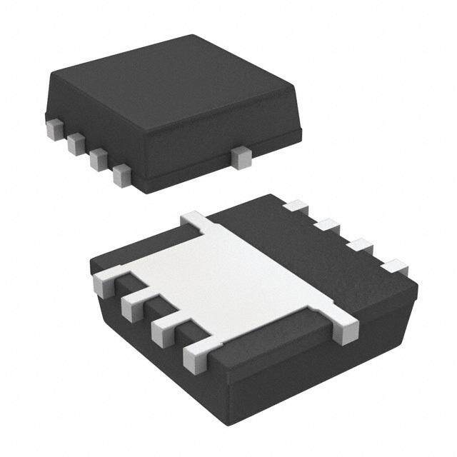
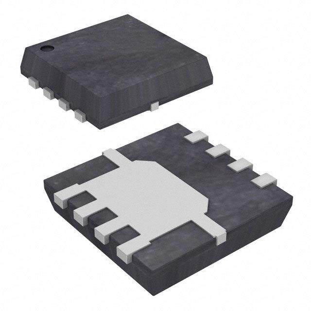
| 产品图片 |
|
| rohs | 符合RoHS无铅 / 符合限制有害物质指令(RoHS)规范要求 |
| 产品系列 | 晶体管,MOSFET,STMicroelectronics STD10NF10T4STripFET™ II |
| 数据手册 | |
| 产品型号 | STD10NF10T4 |
| Pd-PowerDissipation | 50 W |
| Pd-功率耗散 | 50 W |
| RdsOn-Drain-SourceResistance | 115 mOhms |
| RdsOn-漏源导通电阻 | 115 mOhms |
| Vds-Drain-SourceBreakdownVoltage | 100 V |
| Vds-漏源极击穿电压 | 100 V |
| Vgs-Gate-SourceBreakdownVoltage | +/- 20 V |
| Vgs-栅源极击穿电压 | 20 V |
| 上升时间 | 25 ns |
| 下降时间 | 8 ns |
| 不同Id时的Vgs(th)(最大值) | 4V @ 250µA |
| 不同Vds时的输入电容(Ciss) | 460pF @ 25V |
| 不同Vgs时的栅极电荷(Qg) | 21nC @ 10V |
| 不同 Id、Vgs时的 RdsOn(最大值) | 130 毫欧 @ 5A,10V |
| 产品目录页面 | |
| 产品种类 | MOSFET |
| 供应商器件封装 | D-Pak |
| 其它名称 | 497-3153-1 |
| 其它有关文件 | http://www.st.com/web/catalog/sense_power/FM100/CL824/SC1165/PF67183?referrer=70071840 |
| 典型关闭延迟时间 | 32 ns |
| 功率-最大值 | 50W |
| 包装 | 剪切带 (CT) |
| 商标 | STMicroelectronics |
| 安装类型 | 表面贴装 |
| 安装风格 | SMD/SMT |
| 封装 | Reel |
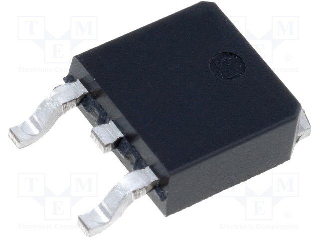
| 封装/外壳 | TO-252-3,DPak(2 引线+接片),SC-63 |
| 封装/箱体 | DPAK-2 |
| 工厂包装数量 | 2500 |
| 晶体管极性 | N-Channel |
| 最大工作温度 | + 175 C |
| 最小工作温度 | - 55 C |
| 标准包装 | 1 |
| 正向跨导-最小值 | 20 S |
| 漏源极电压(Vdss) | 100V |
| 电流-连续漏极(Id)(25°C时) | 13A (Tc) |
| 系列 | STD10NF10 |
| 通道模式 | Enhancement |
| 配置 | Single |


- 商务部:美国ITC正式对集成电路等产品启动337调查
- 曝三星4nm工艺存在良率问题 高通将骁龙8 Gen1或转产台积电
- 太阳诱电将投资9.5亿元在常州建新厂生产MLCC 预计2023年完工
- 英特尔发布欧洲新工厂建设计划 深化IDM 2.0 战略
- 台积电先进制程称霸业界 有大客户加持明年业绩稳了
- 达到5530亿美元!SIA预计今年全球半导体销售额将创下新高
- 英特尔拟将自动驾驶子公司Mobileye上市 估值或超500亿美元
- 三星加码芯片和SET,合并消费电子和移动部门,撤换高东真等 CEO
- 三星电子宣布重大人事变动 还合并消费电子和移动部门
- 海关总署:前11个月进口集成电路产品价值2.52万亿元 增长14.8%

.jpg)

PDF Datasheet 数据手册内容提取
STD10NF10T4 N-channel 100 V, 0.115 Ω typ., 13 A STripFET™ II Power MOSFET in a DPAK package Datasheet - production data Features Order code V R max. I DS DS(on) D STD10NF10T4 100 V 0.130 Ω 13 A Exceptional dv/dt capability Application oriented characterization Applications Switching applications Figure 1: Internal schematic diagram Description D(2, TAB) This Power MOSFET series realized with STMicroelectronics unique STripFET™ process is specifically designed to minimize input capacitance and gate charge. It is therefore ideal as a primary switch in advanced high-efficiency G(1) isolated DC-DC converters for Telecom and Computer applications. It is also suitable for any application with low gate charge drive requirements. S(3) AM01475v1_Tab Table 1: Device summary Order code Marking Package Packing STD10NF10T4 D10NF10 DPAK Tape and reel April 2016 DocID029150 Rev 1 1/17 This is information on a product in full production. www.st.com
Contents STD10NF10T4 Contents 1 Electrical ratings ............................................................................. 3 2 Electrical characteristics ................................................................ 4 2.2 Electrical characteristics (curves) ...................................................... 6 3 Test circuits ..................................................................................... 8 4 Package information ....................................................................... 9 4.1 DPAK (TO-252) type A package information..................................... 9 4.2 DPAK (TO-252) type C package information .................................. 11 4.3 Packing information ......................................................................... 14 5 Revision history ............................................................................ 16 2/17 DocID029150 Rev 1
STD10NF10T4 Electrical ratings 1 Electrical ratings Table 2: Absolute maximum ratings Symbol Parameter Value Unit V Drain-source voltage 100 V DS V Drain-gate voltage (R = 20 kΩ) 100 V DGR GS V Gate-source voltage ±20 V GS I Drain current (continuous) at T = 25 °C 13 A D C I Drain current (continuous) at T = 100 °C 9 A D C I (1) Drain current (pulsed) 52 A DM P Total dissipation at T = 25 °C 50 W TOT C E (2) Single pulse avalanche energy 70 mJ AS dv/dt (3) Peak diode recovery voltage slope 9 V/ns T Operating junction temperature range j - 55 to 175 °C T Storage temperature range stg Notes: (1)Pulse width limited by safe operating area. (2)Starting TJ = 25 °C, ID = 13 A, VDD = 50 V (3)ISD ≤ 13 A, di/dt ≤ 300 A/µs; VDS peak < V(BR)DSS, TJ ≤ TJMAX Table 3: Thermal data Symbol Parameter Value Unit R Thermal resistance junction-case 3 °C/W thj-case R (1) Thermal resistance junction-pcb 50 °C/W thj-pcb Notes: (1)When mounted on 1 inch² FR-4, 2 Oz copper board DocID029150 Rev 1 3/17
Electrical characteristics STD10NF10T4 2 Electrical characteristics T = 25 ° C unless otherwise specified C Table 4: On/off-state Symbol Parameter Test conditions Min. Typ. Max. Unit V Drain-source breakdown voltage V = 0 V, I = 250 µA 100 V (BR)DSS GS D V = 0 V, V = 100 V 1 µA GS DS IDSS Zero gate voltage drain current VGS = 0 V, VDS = 100 V 10 µA TC = 125 °C (1) I Gate body leakage current V =0 V, V ±20 V ± 100 nA GSS DS GS V Gate threshold voltage V = V , I = 250 µA 2 3 4 V GS(th) DS GS D R Static drain-source on-resistance V = 10 V, I = 5 A 0.115 0.130 Ω DS(on) GS D Notes: (1)Defined by design, not subject to production test. Table 5: Dynamic Symbol Parameter Test conditions Min. Typ. Max. Unit C Input capacitance - 460 pF iss C Output capacitance V = 25 V, f = 1 MHz, - 70 pF oss DS V = 0 V Reverse transfer GS C - 30 pF rss capacitance Q Total gate charge V = 80 V, I = 10 A - 15.3 21(1) nC g DD D Qgs Gate-source charge VGS= 10 V - 3.7 nC (see Figure 14: "Test circuit Qgd Gate-drain charge for gate charge behavior" ) - 4.7 nC Notes: (1)Defined by design, not subject to production test. Table 6: Switching times Symbol Parameter Test conditions Min. Typ. Max. Unit t Turn-on delay time - 16 - ns d(on) V = 50 V, I = 5 A, R = 4.7 Ω DD D G tr Rise time VGS = 10 V - 25 - ns t Turn-off delay time (see Figure 13: "Test circuit for - 32 - ns d(off) resistive load switching times") t Fall time - 8 - ns f 4/17 DocID029150 Rev 1
STD10NF10T4 Electrical characteristics Table 7: Source-drain diode Symbol Parameter Test conditions Min. Typ. Max. Unit Source-drain I - 13 A SD current Source-drain I (1) - 52 A SDM current (pulsed) Forward on V (2) I = 10 A, V = 0 V - 1.5 V SD voltage SD GS Reverse recovery trr time ISD = 10 A, di/dt = 100 A/µs, - 90 ns V = 50 V, T= 150 °C Reverse recovery DD j Q - 230 nC rr charge (see Figure 15: "Test circuit for inductive load switching and diode Reverse recovery I recovery times") - 5 A RRM current Notes: (1)Pulse width limited by safe operating area (2)Pulsed: pulse duration = 300 µ s, duty cycle 1.5% DocID029150 Rev 1 5/17
Electrical characteristics STD10NF10T4 2.2 Electrical characteristics (curves) Figure 2: Safe operating area Figure 3: Thermal impedance Figure 4: Output characteristics Figure 5: Transfer characteristics 9 Figure 6: Gate charge vs gate-source voltage Figure 7: Static drain-source on-resistance 6/17 DocID029150 Rev 1
STD10NF10T4 Electrical characteristics Figure 8: Capacitance variations Figure 9: Normalized gate threshold voltage vs temperature Figure 10: Normalized on-resistance vs Figure 11: Normalized V vs temperature (BR)DSS temperature Figure 12: Source-drain diode forward characteristics DocID029150 Rev 1 7/17
Test circuits STD10NF10T4 3 Test circuits Figure 13: Test circuit for resistive load Figure 14: Test circuit for gate charge switching times behavior Figure 15: Test circuit for inductive load Figure 16: Unclamped inductive load test switching and diode recovery times circuit Figure 17: Unclamped inductive waveform Figure 18: Switching time waveform 8/17 DocID029150 Rev 1
STD10NF10T4 Package information 4 Package information In order to meet environmental requirements, ST offers these devices in different grades of ECOPACK® packages, depending on their level of environmental compliance. ECOPACK® specifications, grade definitions and product status are available at: www.st.com. ECOPACK® is an ST trademark. 4.1 DPAK (TO-252) type A package information Figure 19: DPAK (TO-252) type A package outline 0068772_A_21 DocID029150 Rev 1 9/17
Package information STD10NF10T4 Table 8: DPAK (TO-252) type A mechanical data mm Dim. Min. Typ. Max. A 2.20 2.40 A1 0.90 1.10 A2 0.03 0.23 b 0.64 0.90 b4 5.20 5.40 c 0.45 0.60 c2 0.48 0.60 D 6.00 6.20 D1 4.95 5.10 5.25 E 6.40 6.60 E1 4.60 4.70 4.80 e 2.16 2.28 2.40 e1 4.40 4.60 H 9.35 10.10 L 1.00 1.50 (L1) 2.60 2.80 3.00 L2 0.65 0.80 0.95 L4 0.60 1.00 R 0.20 V2 0° 8° 10/17 DocID029150 Rev 1
STD10NF10T4 Package information 4.2 DPAK (TO-252) type C package information Figure 20: DPAK (TO-252) type C package outline 0068772_C_21 DocID029150 Rev 1 11/17
Package information STD10NF10T4 Table 9: DPAK (TO-252) type C mechanical data mm Dim. Min. Typ. Max. A 2.20 2.30 2.38 A1 0.90 1.01 1.10 A2 0.00 0.10 b 0.72 0.85 b4 5.13 5.33 5.46 c 0.47 0.60 c2 0.47 0.60 D 6.00 6.10 6.20 D1 5.25 E 6.50 6.60 6.70 E1 4.70 e 2.186 2.286 2.386 H 9.80 10.10 10.40 L 1.40 1.50 1.70 L1 2.90 REF L2 0.90 1.25 L3 0.51 BSC L4 0.60 0.80 1.00 L6 1.80 BSC θ1 5° 7° 9° θ2 5° 7° 9° V2 0° 8° 12/17 DocID029150 Rev 1
STD10NF10T4 Package information Figure 21: DPAK (TO-252) recommended footprint (dimensions are in mm) FP_0068772_21 DocID029150 Rev 1 13/17
Package information STD10NF10T4 4.3 Packing information Figure 22: DPAK (TO-252) tape outline 14/17 DocID029150 Rev 1
STD10NF10T4 Package information Figure 23: DPAK (TO-252) reel outline Table 10: DPAK (TO-252) tape and reel mechanical data Tape Reel mm mm Dim. Dim. Min. Max. Min. Max. A0 6.8 7 A 330 B0 10.4 10.6 B 1.5 B1 12.1 C 12.8 13.2 D 1.5 1.6 D 20.2 D1 1.5 G 16.4 18.4 E 1.65 1.85 N 50 F 7.4 7.6 T 22.4 K0 2.55 2.75 P0 3.9 4.1 Base qty. 2500 P1 7.9 8.1 Bulk qty. 2500 P2 1.9 2.1 R 40 T 0.25 0.35 W 15.7 16.3 DocID029150 Rev 1 15/17
Revision history STD10NF10T4 5 Revision history Table 11: Document revision history Date Revision Changes 06-Apr-2016 1 First release. 16/17 DocID029150 Rev 1
STD10NF10T4 IMPORTANT NOTICE – PLEASE READ CAREFULLY STMicroelectronics NV and its subsidiaries (“ST”) reserve the right to make changes, corrections, enhancements, modifications, and improvements to ST products and/or to this document at any time without notice. Purchasers should obtain the latest relevant information on ST products before placing orders. ST products are sold pursuant to ST’s terms and conditions of sale in place at the time of order acknowledgement. Purchasers are solely responsible for the choice, selection, and use of ST products and ST assumes no liability for application assistance or the design of Purchasers’ products. No license, express or implied, to any intellectual property right is granted by ST herein. Resale of ST products with provisions different from the information set forth herein shall void any warranty granted by ST for such product. ST and the ST logo are trademarks of ST. All other product or service names are the property of their respective owners. Information in this document supersedes and replaces information previously supplied in any prior versions of this document. © 2016 STMicroelectronics – All rights reserved DocID029150 Rev 1 17/17
Mouser Electronics Authorized Distributor Click to View Pricing, Inventory, Delivery & Lifecycle Information: S TMicroelectronics: STD10NF10T4