ICGOO在线商城 > 分立半导体产品 > 晶体管 - FET,MOSFET - 单 > SI8810EDB-T2-E1
 Datasheet下载
- 型号: SI8810EDB-T2-E1
- 制造商: Vishay
- 库位|库存: xxxx|xxxx
- 要求:
| 数量阶梯 | 香港交货 | 国内含税 |
| +xxxx | $xxxx | ¥xxxx |
查看当月历史价格
查看今年历史价格
SI8810EDB-T2-E1产品简介:
ICGOO电子元器件商城为您提供SI8810EDB-T2-E1由Vishay设计生产,在icgoo商城现货销售,并且可以通过原厂、代理商等渠道进行代购。 SI8810EDB-T2-E1价格参考。VishaySI8810EDB-T2-E1封装/规格:晶体管 - FET,MOSFET - 单, 表面贴装 N 沟道 20V 500mW(Ta) 4-Microfoot。您可以下载SI8810EDB-T2-E1参考资料、Datasheet数据手册功能说明书,资料中有SI8810EDB-T2-E1 详细功能的应用电路图电压和使用方法及教程。
Vishay Siliconix 的 SI8810EDB-T2-E1 是一款 N 沟道增强型 MOSFET,广泛应用于各种电子设备中。以下是其主要应用场景:

 1. 电源管理
   - DC-DC 转换器:该 MOSFET 可用于高效开关电源设计中的功率转换部分,提供低导通电阻(Rds(on))以减少功耗。
   - 负载开关:在便携式设备和消费电子产品中,SI8810EDB-T2-E1 可作为负载开关控制电路的通断,确保快速响应和低损耗。
   - 电池管理系统 (BMS):适用于锂电池保护电路,控制充放电路径。

 2. 电机驱动
   - 小型直流电机控制:可用于驱动风扇、泵或玩具中的小型电机,通过 PWM 调节转速。
   - H 桥电路:与其他 MOSFET 配合,构建 H 桥以实现电机正反转功能。

 3. 信号切换
   - 高速信号切换:由于其快速开关速度,可以用于需要高频切换的应用场景,例如音频放大器或数据通信线路中的信号路由。

 4. 保护电路
   - 过流保护:利用其内置的热关断特性,防止系统因过载而损坏。
   - 短路保护:在某些设计中,可以通过检测 MOSFET 的压降来识别短路情况并采取措施。

 5. 汽车电子
   - 车身控制系统:如车窗升降、座椅调节等辅助功能模块中,作为开关元件使用。
   - LED 照明驱动:为汽车内外部 LED 灯提供稳定的电流驱动。

 6. 工业自动化
   - 传感器接口:用于控制传感器供电或隔离输入输出信号。
   - 继电器替代方案:在一些低电压、低电流场合下,可以用此 MOSFET 替代传统机械继电器,降低噪音并提高可靠性。

总之,SI8810EDB-T2-E1 凭借其优异的电气性能和紧凑封装,适合于对效率、空间和成本敏感的设计项目。具体应用时需根据实际需求选择合适的外围电路配置。
| 参数 | 数值 |
| 产品目录 | |
| 描述 | MOSFET N-CH 20V 2.1A MICROFOOTMOSFET 20V .072ohm@4.5V 2.9A N-Ch |
| 产品分类 | FET - 单分离式半导体 |
| FET功能 | 逻辑电平门 |
| FET类型 | MOSFET N 通道,金属氧化物 |
| Id-ContinuousDrainCurrent | 2.1 A |
| Id-连续漏极电流 | 2.1 A |
| 品牌 | Vishay Siliconix |
| 产品手册 | |
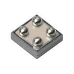
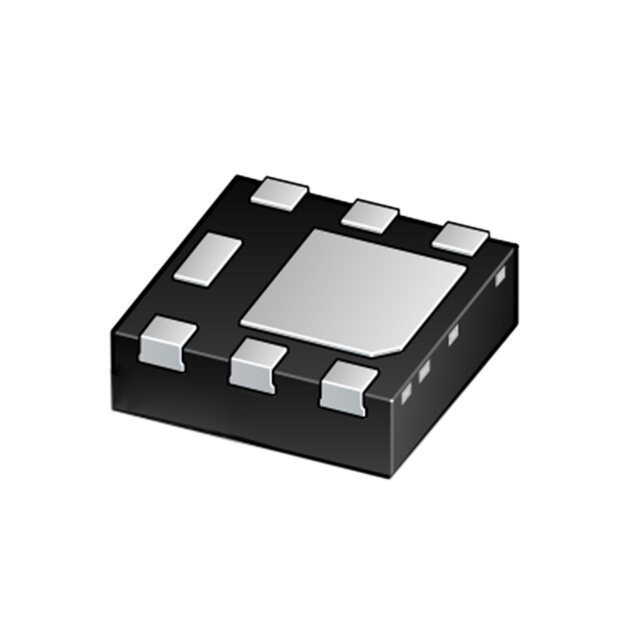
| 产品图片 |
|
| rohs | 符合RoHS无铅 / 符合限制有害物质指令(RoHS)规范要求 |
| 产品系列 | 晶体管,MOSFET,Vishay / Siliconix SI8810EDB-T2-E1TrenchFET® |
| 数据手册 | |
| 产品型号 | SI8810EDB-T2-E1 |
| Pd-PowerDissipation | 500 mW |
| Pd-功率耗散 | 500 mW |
| Qg-GateCharge | 8 nC |
| Qg-栅极电荷 | 8 nC |
| RdsOn-Drain-SourceResistance | 72 mOhms |
| RdsOn-漏源导通电阻 | 72 mOhms |
| Vds-Drain-SourceBreakdownVoltage | 20 V |
| Vds-漏源极击穿电压 | 20 V |
| Vgsth-Gate-SourceThresholdVoltage | 0.9 V |
| Vgsth-栅源极阈值电压 | 0.9 V |
| 上升时间 | 12 ns |
| 下降时间 | 7 ns |
| 不同Id时的Vgs(th)(最大值) | 900mV @ 250µA |
| 不同Vds时的输入电容(Ciss) | 245pF @ 10V |
| 不同Vgs时的栅极电荷(Qg) | 8nC @ 8V |
| 不同 Id、Vgs时的 RdsOn(最大值) | 72 毫欧 @ 1A, 4.5V |
| 产品种类 | MOSFET |
| 供应商器件封装 | 4-Microfoot |
| 其它名称 | SI8810EDB-T2-E1DKR |
| 典型关闭延迟时间 | 25 ns |
| 功率-最大值 | 500mW |
| 包装 | Digi-Reel® |
| 商标 | Vishay / Siliconix |
| 安装类型 | 表面贴装 |
| 安装风格 | SMD/SMT |
| 封装 | Reel |
| 封装/外壳 | 4-XFBGA |
| 封装/箱体 | XFBGA-4 |
| 工厂包装数量 | 3000 |
| 晶体管极性 | N-Channel |
| 最大工作温度 | + 150 C |
| 最小工作温度 | - 55 C |
| 标准包装 | 1 |
| 正向跨导-最小值 | 12 S |
| 漏源极电压(Vdss) | 20V |
| 电流-连续漏极(Id)(25°C时) | - |


- 商务部:美国ITC正式对集成电路等产品启动337调查
- 曝三星4nm工艺存在良率问题 高通将骁龙8 Gen1或转产台积电
- 太阳诱电将投资9.5亿元在常州建新厂生产MLCC 预计2023年完工
- 英特尔发布欧洲新工厂建设计划 深化IDM 2.0 战略
- 台积电先进制程称霸业界 有大客户加持明年业绩稳了
- 达到5530亿美元!SIA预计今年全球半导体销售额将创下新高
- 英特尔拟将自动驾驶子公司Mobileye上市 估值或超500亿美元
- 三星加码芯片和SET,合并消费电子和移动部门,撤换高东真等 CEO
- 三星电子宣布重大人事变动 还合并消费电子和移动部门
- 海关总署:前11个月进口集成电路产品价值2.52万亿元 增长14.8%


PDF Datasheet 数据手册内容提取
Si8810EDB www.vishay.com Vishay Siliconix N-Channel 20 V (D-S) MOSFET FEATURES PRODUCT SUMMARY • TrenchFET® power MOSFET V (V) R (Ω) MAX. I (A) a Q (TYP.) DS DS(on) D g • Ultra small 0.8 mm x 0.8 mm outline 0.072 at V = 4.5 V 2.9 GS • Ultra thin 0.357 mm height 0.079 at V = 2.5 V 2.8 20 GS 3 nC • Typical ESD protection 2000 V (HBM) 0.092 at V = 1.8 V 2.6 GS • Material categorization: for definitions of 0.125 at VGS = 1.5 V 2.2 compliance please see www.vishay.com/doc?99912 MICRO FOOT® 0.8 x 0.8 APPLICATIONS S 22 • Portable devices such as cell phones, D SS x 33 smart phones, and tablet PCs x x x - Load switch x - Small signal switch G 0. 11 8 mm 1 0.8 m m 44 GG - High speed switching D Backside View Bump Side View Marking Code: xx = AJ S xxx = Date/Lot traceability code N-Channel MOSFET Ordering Information: Si8810EDB-T2-E1 (lead (Pb)-free and halogen-free) ABSOLUTE MAXIMUM RATINGS (T = 25 °C, unless otherwise noted) A PARAMETER SYMBOL LIMIT UNIT Drain-Source Voltage V 20 DS V Gate-Source Voltage V ± 8 GS T = 25 °C 2.9 a A T = 70 °C 2.3 a A Continuous Drain Current (T = 150 °C) I J T = 25 °C D 2.1 b A T = 70 °C 1.7 b A A Pulsed Drain Current (t = 300 μs) I 15 DM T = 25 °C 0.7 a A Continuous Source-Drain Diode Current I T = 25 °C S 0.4 b A T = 25 °C 0.9 a A T = 70 °C 0.6 a A Maximum Power Dissipation P W T = 25 °C D 0.5 b A T = 70 °C 0.3 b A Operating Junction and Storage Temperature Range T , T -55 to +150 J stg °C Soldering Recommendations (Peak Temperature) c 260 THERMAL RESISTANCE RATINGS PARAMETER SYMBOL TYPICAL MAXIMUM UNIT Maximum Junction-to-Ambient a, d 105 135 t ≤ 5 s R °C/W Maximum Junction-to-Ambient b, e thJA 200 260 Notes a. Surface mounted on 1" x 1" FR4 board with full copper, t = 5 s. b. Surface mounted on 1" x 1" FR4 board with minimum copper, t = 5 s. c. Refer to IPC/JEDEC® (J-STD-020), no manual or hand soldering. d. Maximum under steady state conditions is 185 °C/W. e. Maximum under steady state conditions is 330 °C/W. S15-0346-Rev. B, 23-Feb-15 1 Document Number: 62829 For technical questions, contact: pmostechsupport@vishay.com THIS DOCUMENT IS SUBJECT TO CHANGE WITHOUT NOTICE. THE PRODUCTS DESCRIBED HEREIN AND THIS DOCUMENT ARE SUBJECT TO SPECIFIC DISCLAIMERS, SET FORTH AT www.vishay.com/doc?91000
Si8810EDB www.vishay.com Vishay Siliconix SPECIFICATIONS (T = 25 °C, unless otherwise noted) J PARAMETER SYMBOL TEST CONDITIONS MIN. TYP. MAX. UNIT Static Drain-Source Breakdown Voltage V V = 0 V, I = 250 μA 20 - - V DS GS D V Temperature Coefficient ΔV /T - 21 - DS DS J I = 250 μA mV/°C V Temperature Coefficient ΔV /T D - -2.7 - GS(th) GS(th) J Gate-Source Threshold Voltage V V = V , I = 250 μA 0.4 - 0.9 V GS(th) DS GS D V = 0 V, V = ± 4.5 V - - ± 0.5 DS GS Gate-Source Leakage I GSS V = 0 V, V = ± 8 V - - ± 5 DS GS μA V = 20 V, V = 0 V - - 1 DS GS Zero Gate Voltage Drain Current I DSS V = 20 V, V = 0 V, T = 55 °C - - 10 DS GS J On-State Drain Current a I V ≥ 5 V, V = 4.5 V 10 - - A D(on) DS GS V = 4.5 V, I = 1 A - 0.058 0.072 GS D V = 2.5 V, I = 1 A - 0.063 0.079 Drain-Source On-State Resistance a R GS D Ω DS(on) V = 1.8 V, I = 1 A - 0.072 0.092 GS D V = 1.5 V, I = 0.5 A - 0.080 0.125 GS D Forward Transconductance a g V = 10 V, I = 1 A - 12 - S fs DS D Dynamic b Input Capacitance C - 245 - iss Output Capacitance C V = 10 V, V = 0 V, f = 1 MHz - 55 - pF oss DS GS Reverse Transfer Capacitance C - 25 - rss V = 10 V, V = 8 V, I = 1 A - 5.2 8 DS GS D Total Gate Charge Q g - 3 4.5 nC Gate-Source Charge Q V = 10 V, V = 4.5 V, I = 1 A - 0.35 - gs DS GS D Gate-Drain Charge Q - 0.45 - gd Gate Resistance R f = 1 MHz - 5 - Ω g Turn-On Delay Time t - 7 15 d(on) Rise Time tr VDD = 10 V, RL = 10 Ω - 12 25 Turn-Off Delay Time td(off) ID ≅ 1 A, VGEN = 4.5 V, Rg = 1 Ω - 25 50 Fall Time t - 7 15 f ns Turn-On Delay Time t - 5 10 d(on) Rise Time tr VDD = 10 V, RL = 10 Ω - 10 20 Turn-Off Delay Time td(off) ID ≅ 1 A, VGEN = 8 V, Rg = 1 Ω - 15 30 Fall Time t - 7 15 f Drain-Source Body Diode Characteristics Continuous Source-Drain Diode Current I T = 25 °C - - 0.7 S C A Pulse Diode Forward Current I - - 15 SM Body Diode Voltage V I = 1 A, V = 0 V - 0.7 1.2 V SD S GS Body Diode Reverse Recovery Time t - 11 20 ns rr Body Diode Reverse Recovery Charge Q - 5 10 nC rr I = 1 A, dI/dt = 100 A/μs, T = 25 °C F J Reverse Recovery Fall Time t - 7 - a ns Reverse Recovery Rise Time t - 4 - b Notes a. Pulse test; pulse width ≤ 300 μs, duty cycle ≤ 2 %. b. Guaranteed by design, not subject to production testing. Stresses beyond those listed under “Absolute Maximum Ratings” may cause permanent damage to the device. These are stress ratings only, and functional operation of the device at these or any other conditions beyond those indicated in the operational sections of the specifications is not implied. Exposure to absolute maximum rating conditions for extended periods may affect device reliability. S15-0346-Rev. B, 23-Feb-15 2 Document Number: 62829 For technical questions, contact: pmostechsupport@vishay.com THIS DOCUMENT IS SUBJECT TO CHANGE WITHOUT NOTICE. THE PRODUCTS DESCRIBED HEREIN AND THIS DOCUMENT ARE SUBJECT TO SPECIFIC DISCLAIMERS, SET FORTH AT www.vishay.com/doc?91000
Si8810EDB www.vishay.com Vishay Siliconix TYPICAL CHARACTERISTICS (25 °C, unless otherwise noted) 2.50 1 0-2 1 0-3 2.00 urrent (mA) 1.50 TJ = 25 °C Current (A) 11 00--45 TJ = 150 °C ate C 1.00 Gate 1 0-6 TJ = 25 °C - GGSS I - GSS 1 0-7 I 0.50 1 0-8 0.00 1 0-9 0 4 8 12 16 0 4 8 12 16 VGS - Gate-Source Voltage (V) VGS - Gate-to-Source Voltage (V) Gate Current vs. Gate-Source Voltage Gate Current vs. Gate-Source Voltage 15 10 V = 5 V thru 2 V GS 12 8 Current (A) 9 VGS = 1.5 V urrent (A) 6 ain n C I Dr -D 6 - DraiD 4 TC = 25 °C I 3 2 TC = 125 °C VGS = 1 V TC = - 55 °C 0 0 0.0 0.5 1.0 1.5 2.0 2.5 3.0 0.0 0.5 1.0 1.5 2.0 VDS - Drain-to-Source Voltage (V) VGS - Gate-to-Source Voltage (V) Output Characteristics Transfer Characteristics 0.200 350 V = 1.5 V GS 300 0.160 Ω) Ciss e ( F) 250 R - On-ResistancDS(on) 00..018200 V = 4.5 V VGS = 1.8 V C - Capacitance (p 112050000 Coss 0.040 GS V = 2.5 V GS 50 Crss 0.000 0 0 3 6 9 12 15 0 2 4 6 8 10 12 ID - Drain Current (A) VDS - Drain-to-Source Voltage (V) On-Resistance vs. Drain Current Capacitance vs. Drain-to-Source Voltage S15-0346-Rev. B, 23-Feb-15 3 Document Number: 62829 For technical questions, contact: pmostechsupport@vishay.com THIS DOCUMENT IS SUBJECT TO CHANGE WITHOUT NOTICE. THE PRODUCTS DESCRIBED HEREIN AND THIS DOCUMENT ARE SUBJECT TO SPECIFIC DISCLAIMERS, SET FORTH AT www.vishay.com/doc?91000
Si8810EDB www.vishay.com Vishay Siliconix TYPICAL CHARACTERISTICS (25 °C, unless otherwise noted) 8 100 V) ID = 1 A VDS = 6 V ge ( 6 A) TJ = 150 °C e Volta VDS = 3 V urrent ( 10 c C o-Sour 4 VDS = 9.6 V ource TJ = 25 °C - Gate-tGS 2 I - SS 1 V 0 0.1 0 1 2 3 4 5 6 0.0 0.2 0.4 0.6 0.8 1.0 1.2 Q - Total Gate Charge (nC) V - Source-to-Drain Voltage (V) g SD Gate Charge Source-Drain Diode Forward Voltage 1.5 0.8 V = 4.5 V, 3.7 V, 2.5 V; I = 1A GS D zed) 1.4 VGS = 1.5 V; ID = 0.5A 0.7 ali m 1.3 or 0.6 N ce ( 1.2 V) Resistan 1.1 V (GS(th) 0.5 ID = 250 μA n- 0.4 O R - DS(on) 01..90 0.3 0.8 0.2 - 50 - 25 0 25 50 75 100 125 150 - 50 - 25 0 25 50 75 100 125 150 TJ - Junction Temperature (°C) TJ - Temperature (°C) On-Resistance vs. Junction Temperature Threshold Voltage 0.200 14 12 I = 1 A 0.160 D e (Ω) 10 c n-Resistan0.120 TJ = 125 °C Power (W) 68 O0.080 R - DS(on)0.040 TJ = 25 °C 4 2 0.000 0 0 1 2 3 4 5 0.001 0.01 0.1 1 10 100 1000 V - Gate-to-Source Voltage (V) Time (s) GS On-Resistance vs. Gate-to-Source Voltage Single Pulse Power (Junction-to-Ambient) S15-0346-Rev. B, 23-Feb-15 4 Document Number: 62829 For technical questions, contact: pmostechsupport@vishay.com THIS DOCUMENT IS SUBJECT TO CHANGE WITHOUT NOTICE. THE PRODUCTS DESCRIBED HEREIN AND THIS DOCUMENT ARE SUBJECT TO SPECIFIC DISCLAIMERS, SET FORTH AT www.vishay.com/doc?91000
Si8810EDB www.vishay.com Vishay Siliconix TYPICAL CHARACTERISTICS (25 °C, unless otherwise noted) 100 Limited by R * DS(on) 10 A) nt ( 100 µs e urr C 1 n 1 ms ai Dr I - D 100 ms 0.1 T = 25 °C 10 s A 1 s, 10 ms DC BVDSS Limited 0.01 0.1 1 10 100 V - Drain-to-Source Voltage (V) DS * V > minimum V at which R is specified GS GS DS(on) Safe Operating Area, Junction-to-Ambient 3.0 0.8 2.5 0.6 nt (A) 2.0 on (W) Curre 1.5 sipati 0.4 Drain er Dis I - D 1.0 Pow 0.2 0.5 0.0 0.0 0 25 50 75 100 125 150 25 50 75 100 125 150 TA - Ambient Temperature (°C) TA-Ambient Temperature(°C) Current Derating* Power Derating Note When mounted on 1" x 1" FR4 with full copper. * The power dissipation P is based on T = 150 °C, using junction-to-case thermal resistance, and is more useful in settling the upper D J (max.) dissipation limit for cases where additional heatsinking is used. It is used to determine the current rating, when this rating falls below the package limit. S15-0346-Rev. B, 23-Feb-15 5 Document Number: 62829 For technical questions, contact: pmostechsupport@vishay.com THIS DOCUMENT IS SUBJECT TO CHANGE WITHOUT NOTICE. THE PRODUCTS DESCRIBED HEREIN AND THIS DOCUMENT ARE SUBJECT TO SPECIFIC DISCLAIMERS, SET FORTH AT www.vishay.com/doc?91000
Si8810EDB www.vishay.com Vishay Siliconix TYPICAL CHARACTERISTICS (25 °C, unless otherwise noted) 1 DutyCycle=0.5 nt e Transiance 0.2 ctivemped 0.1 Notes: edEffeermalI 0.1 0.05 PDM zh maliT 0.02 t1 Nor 1.DutyCyclet,2D= t1 t2 2.PerUnitBase=RthJA=185 °C/W 3.TJM-TA=PDMZthJA(t) SinglePulse 4.SurfaceMounted 0.01 10-4 10-3 10-2 10-1 1 10 100 1000 SquareWavePulseDuration(s) Normalized Thermal Transient Impedance, Junction-to-Ambient (on 1" x 1" FR4 board with maximum copper) 1 DutyCycle=0.5 nt e Transiance 0.2 ctivemped 0.1 Notes: edEffeermalI 0.1 0.05 PDM zh maliT t1 Nor 0.02 1.DutyCyclet,2D= t1 t2 2.PerUnitBase=RthJA=330 °C/W SinglePulse 3.TJM-TA=PDMZthJA(t) 4.SurfaceMounted 0.01 10-4 10-3 10-2 10-1 1 10 100 1000 SquareWavePulseDuration(s) Normalized Thermal Transient Impedance, Junction-to-Ambient (on 1" x 1" FR4 board with minimum copper) Vishay Siliconix maintains worldwide manufacturing capability. Products may be manufactured at one of several qualified locations. Reliability data for Silicon Technology and Package Reliability represent a composite of all qualified locations. For related documents such as package/tape drawings, part marking, and reliability data, see www.vishay.com/ppg?62829. S15-0346-Rev. B, 23-Feb-15 6 Document Number: 62829 For technical questions, contact: pmostechsupport@vishay.com THIS DOCUMENT IS SUBJECT TO CHANGE WITHOUT NOTICE. THE PRODUCTS DESCRIBED HEREIN AND THIS DOCUMENT ARE SUBJECT TO SPECIFIC DISCLAIMERS, SET FORTH AT www.vishay.com/doc?91000
Package Information www.vishay.com Vishay Siliconix MICRO FOOT®: 4-Bump (0.8 mm x 0.8 mm, 0.4 mm Pitch) D S e S 4x Ø b XXX S S S e D G D AK S Mark on Backside of die 4-Ø 0.205 to 0.225 Note 5 Solder Mask ~Ø 0.215 b A2 e A 1 A b1 k Bump Note 2 e Note 4 Notes (1) Laser mark on the backside surface of die (2) Bumps are 95.5 % Sn,3.8 % Ag,0.7 % Cu (3) “i” is the location of pin 1 (4) “b1” is the diameter of the solderable substrate surface, defined by an opening in the solder resist layer solder mask defined. (5) Non-solder mask defined copper landing pad. MILLIMETERS a INCHES DIM. MIN. NOM. MAX. MIN. NOM. MAX. A 0.328 0.365 0.402 0.0129 0.0144 0.0158 A1 0.136 0.160 0.184 0.0053 0.0062 0.0072 A2 0.192 0.205 0.218 0.0076 0.0081 0.0086 b 0.200 0.220 0.240 0.0078 0.0086 0.0094 b1 0.175 0.0068 e 0.400 0.0157 S 0.160 0.180 0.200 0.0062 0.0070 0.0078 D 0.720 0.760 0.800 0.0283 0.0299 0.0314 K 0.040 0.070 0.100 0.0015 0.0027 0.0039 Note a. Use millimeters as the primary measurement. ECN: T15-0053-Rev. A, 16-Feb-15 DWG: 6033 Revision: 16-Feb-15 1 Document Number: 69442 THIS DOCUMENT IS SUBJECT TO CHANGE WITHOUT NOTICE. THE PRODUCTS DESCRIBED HEREIN AND THIS DOCUMENT ARE SUBJECT TO SPECIFIC DISCLAIMERS, SET FORTH AT www.vishay.com/doc?91000
Legal Disclaimer Notice www.vishay.com Vishay Disclaimer ALL PRODUCT, PRODUCT SPECIFICATIONS AND DATA ARE SUBJECT TO CHANGE WITHOUT NOTICE TO IMPROVE RELIABILITY, FUNCTION OR DESIGN OR OTHERWISE. Vishay Intertechnology, Inc., its affiliates, agents, and employees, and all persons acting on its or their behalf (collectively, “Vishay”), disclaim any and all liability for any errors, inaccuracies or incompleteness contained in any datasheet or in any other disclosure relating to any product. Vishay makes no warranty, representation or guarantee regarding the suitability of the products for any particular purpose or the continuing production of any product. To the maximum extent permitted by applicable law, Vishay disclaims (i) any and all liability arising out of the application or use of any product, (ii) any and all liability, including without limitation special, consequential or incidental damages, and (iii) any and all implied warranties, including warranties of fitness for particular purpose, non-infringement and merchantability. Statements regarding the suitability of products for certain types of applications are based on Vishay’s knowledge of typical requirements that are often placed on Vishay products in generic applications. Such statements are not binding statements about the suitability of products for a particular application. It is the customer’s responsibility to validate that a particular product with the properties described in the product specification is suitable for use in a particular application. Parameters provided in datasheets and / or specifications may vary in different applications and performance may vary over time. All operating parameters, including typical parameters, must be validated for each customer application by the customer’s technical experts. Product specifications do not expand or otherwise modify Vishay’s terms and conditions of purchase, including but not limited to the warranty expressed therein. Except as expressly indicated in writing, Vishay products are not designed for use in medical, life-saving, or life-sustaining applications or for any other application in which the failure of the Vishay product could result in personal injury or death. Customers using or selling Vishay products not expressly indicated for use in such applications do so at their own risk. Please contact authorized Vishay personnel to obtain written terms and conditions regarding products designed for such applications. No license, express or implied, by estoppel or otherwise, to any intellectual property rights is granted by this document or by any conduct of Vishay. Product names and markings noted herein may be trademarks of their respective owners. © 2017 VISHAY INTERTECHNOLOGY, INC. ALL RIGHTS RESERVED Revision: 08-Feb-17 1 Document Number: 91000
Mouser Electronics Authorized Distributor Click to View Pricing, Inventory, Delivery & Lifecycle Information: V ishay: SI8810EDB-T2-E1