ICGOO在线商城 > 分立半导体产品 > 晶体管 - FET,MOSFET - 单 > SI2337DS-T1-E3
 Datasheet下载
- 型号: SI2337DS-T1-E3
- 制造商: Vishay
- 库位|库存: xxxx|xxxx
- 要求:
| 数量阶梯 | 香港交货 | 国内含税 |
| +xxxx | $xxxx | ¥xxxx |
查看当月历史价格
查看今年历史价格
SI2337DS-T1-E3产品简介:
ICGOO电子元器件商城为您提供SI2337DS-T1-E3由Vishay设计生产,在icgoo商城现货销售,并且可以通过原厂、代理商等渠道进行代购。 SI2337DS-T1-E3价格参考¥2.03-¥2.03。VishaySI2337DS-T1-E3封装/规格:晶体管 - FET,MOSFET - 单, P-Channel 80V 2.2A (Tc) 760mW (Ta), 2.5W (Tc) Surface Mount SOT-23-3 (TO-236)。您可以下载SI2337DS-T1-E3参考资料、Datasheet数据手册功能说明书,资料中有SI2337DS-T1-E3 详细功能的应用电路图电压和使用方法及教程。
Vishay Siliconix 的 SI2337DS-T1-E3 是一款P沟道增强型MOSFET,采用SOT-23封装,具有低导通电阻、小尺寸和高可靠性等特点。该器件广泛应用于便携式电子设备和电源管理领域。

典型应用场景包括:手机、平板电脑、笔记本电脑等消费类电子产品中的电源开关和负载开关,用于控制电池供电路径或模块供电,实现低功耗管理和节能。其P沟道特性无需额外驱动电路即可实现高边或低边开关功能,简化设计。

此外,SI2337DS-T1-E3也适用于DC-DC转换器中的同步整流、电压反转电路及电机驱动中的开关控制,提升系统效率。在热插拔电路和过流保护模块中,可作为理想的开关元件,提供快速响应和稳定性能。

由于其符合RoHS标准且可靠性高,该型号还广泛用于工业控制、通信设备和便携式医疗设备中,适合对空间和功耗敏感的应用场合。总体而言,SI2337DS-T1-E3是一款高性能、低成本的通用型P沟道MOSFET,适用于多种中低功率开关场景。
| 参数 | 数值 |
| 产品目录 | |
| ChannelMode | Enhancement |
| 描述 | MOSFET P-CH 80V 2.2A SOT23-3MOSFET 80V 2.2A 2.5W |
| 产品分类 | FET - 单分离式半导体 |
| FET功能 | 逻辑电平门 |
| FET类型 | MOSFET P 通道,金属氧化物 |
| Id-ContinuousDrainCurrent | 1.2 A |
| Id-连续漏极电流 | 1.2 A |
| 品牌 | Vishay / SiliconixVishay Siliconix |
| 产品手册 | |
| 产品图片 |
|
| rohs | 符合RoHS无铅 / 符合限制有害物质指令(RoHS)规范要求 |
| 产品系列 | 晶体管,MOSFET,Vishay / Siliconix SI2337DS-T1-E3TrenchFET® |
| 数据手册 | |
| 产品型号 | SI2337DS-T1-E3SI2337DS-T1-E3 |
| Pd-PowerDissipation | 760 mW |
| Pd-功率耗散 | 760 mW |
| RdsOn-Drain-SourceResistance | 270 mOhms |
| RdsOn-漏源导通电阻 | 270 mOhms |
| Vds-Drain-SourceBreakdownVoltage | 80 V |
| Vds-漏源极击穿电压 | - 80 V |
| Vgs-Gate-SourceBreakdownVoltage | +/- 20 V |
| Vgs-栅源极击穿电压 | 20 V |
| 上升时间 | 15 ns |
| 下降时间 | 15 ns |
| 不同Id时的Vgs(th)(最大值) | 4V @ 250µA |
| 不同Vds时的输入电容(Ciss) | 500pF @ 40V |
| 不同Vgs时的栅极电荷(Qg) | 17nC @ 10V |
| 不同 Id、Vgs时的 RdsOn(最大值) | 270 毫欧 @ 1.2A,10V |
| 产品目录页面 | |
| 产品种类 | MOSFET |
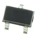
| 供应商器件封装 | SOT-23-3(TO-236) |
| 其它名称 | SI2337DS-T1-E3CT |
| 典型关闭延迟时间 | 20 ns |
| 功率-最大值 | 2.5W |
| 包装 | 剪切带 (CT) |
| 商标 | Vishay / Siliconix |
| 安装类型 | 表面贴装 |
| 安装风格 | SMD/SMT |
| 封装 | Reel |
| 封装/外壳 | TO-236-3,SC-59,SOT-23-3 |
| 封装/箱体 | SOT-23-3 |
| 工厂包装数量 | 3000 |
| 晶体管极性 | P-Channel |
| 最大工作温度 | + 150 C |
| 最小工作温度 | - 55 C |
| 标准包装 | 1 |
| 漏源极电压(Vdss) | 80V |
| 电流-连续漏极(Id)(25°C时) | 2.2A (Tc) |
| 通道模式 | Enhancement |
| 配置 | Single |
| 零件号别名 | SI2337DS-E3 |


.jpg)


- 商务部:美国ITC正式对集成电路等产品启动337调查
- 曝三星4nm工艺存在良率问题 高通将骁龙8 Gen1或转产台积电
- 太阳诱电将投资9.5亿元在常州建新厂生产MLCC 预计2023年完工
- 英特尔发布欧洲新工厂建设计划 深化IDM 2.0 战略
- 台积电先进制程称霸业界 有大客户加持明年业绩稳了
- 达到5530亿美元!SIA预计今年全球半导体销售额将创下新高
- 英特尔拟将自动驾驶子公司Mobileye上市 估值或超500亿美元
- 三星加码芯片和SET,合并消费电子和移动部门,撤换高东真等 CEO
- 三星电子宣布重大人事变动 还合并消费电子和移动部门
- 海关总署:前11个月进口集成电路产品价值2.52万亿元 增长14.8%


PDF Datasheet 数据手册内容提取
Si2337DS www.vishay.com Vishay Siliconix P-Channel 80-V (D-S) MOSFET FEATURES PRODUCT SUMMARY • TrenchFET® power MOSFET V (V) R (Ω) I (A) a Q (TYP.) DS DS(on) D g • Material categorization: 0.270 at V = -10 V -2.2 GS -80 7 for definitions of compliance please see 0.303 at V = -6 V -2.1 GS www.vishay.com/doc?99912 SOT-23 (TO-236) Available S D 3 G 2 S 1 G D Top View Marking Code: E7 P-Channel MOSFET Ordering Information: Si2337DS-T1-E3 (Lead (Pb)-free) Si2337DS-T1-GE3 (Lead (Pb)-free and halogen-free) ABSOLUTE MAXIMUM RATINGS (T = 25 °C, unless otherwise noted) A PARAMETER SYMBOL LIMIT UNIT Drain-Source Voltage V -80 DS V Gate-Source Voltage V ± 20 GS T = 25 °C -2.2 C T = 70 °C -1.75 C Continuous Drain Current (T = 150 °C) I J T = 25 °C D -1.2 b, c A T = 70 °C -0.96 b, c A A Pulsed Drain Current I -7 DM T = 25 °C -2.1 C Continuous Source-Drain Diode Current I T = 25 °C S -0.63 b, c A Avalanche Current I 11 AS L = 0.1 mH Single-Pulse Avalanche Energy E 6 mJ AS T = 25 °C 2.5 C T = 70 °C 1.6 C Maximum Power Dissipation P W T = 25 °C D 0.76 b, c A T = 70 °C 0.48 b, c A Operating Junction and Storage Temperature Range T , T -50 to +150 J stg °C Soldering Recommendations (Peak Temperature) d, e 260 THERMAL RESISTANCE RATINGS PARAMETER SYMBOL TYPICAL MAXIMUM UNIT Maximum Junction-to-Ambient b, d t ≤ 10 s R 120 166 thJA °C/W Maximum Junction-to-Foot (Drain) Steady State R 40 50 thJF Notes a. Package limited. b. Surface mounted on 1" x 1" FR4 board. c. t = 10 s. d. Maximum under Steady State conditions is 166 °C/W. S15-0683-Rev. E, 06-Apr-15 1 Document Number: 73533 For technical questions, contact: pmostechsupport@vishay.com THIS DOCUMENT IS SUBJECT TO CHANGE WITHOUT NOTICE. THE PRODUCTS DESCRIBED HEREIN AND THIS DOCUMENT ARE SUBJECT TO SPECIFIC DISCLAIMERS, SET FORTH AT www.vishay.com/doc?91000
Si2337DS www.vishay.com Vishay Siliconix SPECIFICATIONS (T = 25 °C, unless otherwise noted) J PARAMETER SYMBOL TEST CONDITIONS MIN. TYP. MAX. UNIT Static Drain-Source Breakdown Voltage V V = 0 V, I = -250 μA -80 - - V DS GS D V Temperature Coefficient ΔV /T - -35.8 - DS DS J I = -250 μA mV/°C V Temperature Coefficient ΔVG /T D - 5.45 - GS(th) S(th) J Gate-Source Threshold Voltage V V = V , I = -250 μA -2 - -4 V GS(th) DS GS D Gate-Source Leakage I V = 0 V, V = ± 20 V - - ± 100 nA GSS DS GS V = -80 V, V = 0 V - - -1 DS GS Zero Gate Voltage Drain Current I μA DSS V = -80 V, V = 0 V, T = 55 °C - - -10 DS GS J On-State Drain Current a I V ≥ 5 V, V = -10 V -7 - - A D(on) DS GS V = -10 V, I = -1.2 A - 0.216 0.270 Drain-Source On-State Resistance a R GS D Ω DS(on) V = -6 V, I = -1.1 A - 0.242 0.303 GS D Forward Transconductance a g V = -15 V, I = -1.2 A - 4.3 - S fs DS D Dynamic b Input Capacitance C - 500 - iss Output Capacitance C V = -40 V, V = 0 V, f = 1 MHz - 40 - pF oss DS GS Reverse Transfer Capacitance C - 25 - rss V = -40 V, V = -10 V, I = -1.2 A - 11 17 DS GS D Total Gate Charge Q g - 7 11 nC Gate-Source Charge Q V = -40 V, V = -6 V, I = -1.2 A - 2.1 - gs DS GS D Gate-Drain Charge Q - 3.2 - gd Gate Resistance R f = 1 MHz - 4.8 - Ω g Turn-On Delay Time t - 10 15 d(on) Rise Time tr VDD = -40 V, RL = 42 Ω - 15 23 Turn-Off Delay Time td(off) ID ≅ -0.96 A, VGEN = -10 V, Rg = 1 Ω - 20 30 Fall Time t - 15 23 f ns Turn-On Delay Time t - 15 23 d(on) Rise Time tr VDD = -40 V, RL = 42 Ω - 18 27 Turn-Off Delay Time td(off) ID ≅ -0.96 A, VGEN = -6 V, Rg = 1 Ω - 20 30 Fall Time t - 12 18 f Drain-Source Body Diode Characteristics Continuous Source-Drain Diode Current I T = 25 °C - - -2.1 S C A Pulse Diode Forward Current a I - - -7 SM Body Diode Voltage V I = 0.63 A - -0.8 -1.2 V SD S Body Diode Reverse Recovery Time t - 30 45 ns rr Body Diode Reverse Recovery Charge Q - 45 70 nC rr I = 0.63 A, dI/dt = 100 A/μs, T = 25 °C F J Reverse Recovery Fall Time t - 25 - a ns Reverse Recovery Rise Time t - 5 - b Notes a. Pulse test; pulse width ≤ 300 μs, duty cycle ≤ 2 %. b. Guaranteed by design, not subject to production testing. Stresses beyond those listed under “Absolute Maximum Ratings” may cause permanent damage to the device. These are stress ratings only, and functional operation of the device at these or any other conditions beyond those indicated in the operational sections of the specifications is not implied. Exposure to absolute maximum rating conditions for extended periods may affect device reliability. S15-0683-Rev. E, 06-Apr-15 2 Document Number: 73533 For technical questions, contact: pmostechsupport@vishay.com THIS DOCUMENT IS SUBJECT TO CHANGE WITHOUT NOTICE. THE PRODUCTS DESCRIBED HEREIN AND THIS DOCUMENT ARE SUBJECT TO SPECIFIC DISCLAIMERS, SET FORTH AT www.vishay.com/doc?91000
Si2337DS www.vishay.com Vishay Siliconix TYPICAL CHARACTERISTICS (25 °C, unless otherwise noted) 7 7 VGS = 10 thru 6 V 6 6 )A 5 VGS = 5 V )A 5 ( tn ( tn erru 4 erru 4 C C n n ia 3 ia 3 rD -ID 2 rD -ID 2 TA = - 55 °C TA = 25 °C 1 VGS = 4 V 1 TA = 125 °C 0 0 0 1 2 3 4 0.0 1.0 2.0 3.0 4.0 5.0 VDS - Drain-to-Source Voltage (V) VGS - Gate-to-Source Voltage (V) Output Characteristics Transfer Characteristics 0.30 700 600 () ec 0.25 VGS = 6 V )F 500 Ciss n p ReatsisR-nO -)no(SD 00..1250 VGS = 10 V i- CnaapaC( ectc 234000000 100 Coss 0.10 0 Crss 0 1 2 3 4 5 6 7 0 10 20 30 40 50 60 70 80 ID - Drain Current (A) VDS - Drain-to-Source Voltage (V) On-Resistance vs. Drain Current and Gate Voltage Capacitance 10 2.0 t lo)VegaV( 8 ID =1.2 A VDS = 40 V )eziamro(dlN 111...468 ID = 1.2 A VGS = 10 VVGS = 6 V e 6 e c c uoSot-eaGr-t -VSG 24 VDS = 64 V eRnntO - asis-)oSn( 011...802 D R 0.6 0 0.4 0 2 4 6 8 10 12 - 50 - 25 0 25 50 75 100 125 150 Qg - Total Gate Charge (nC) TJ- Junction Temperature (°C) Gate Charge On-Resistance vs. Junction Temperature S15-0683-Rev. E, 06-Apr-15 3 Document Number: 73533 For technical questions, contact: pmostechsupport@vishay.com THIS DOCUMENT IS SUBJECT TO CHANGE WITHOUT NOTICE. THE PRODUCTS DESCRIBED HEREIN AND THIS DOCUMENT ARE SUBJECT TO SPECIFIC DISCLAIMERS, SET FORTH AT www.vishay.com/doc?91000
Si2337DS www.vishay.com Vishay Siliconix TYPICAL CHARACTERISTICS (25 °C, unless otherwise noted) 20 0.6 ) ID = 1.2 A 10 ( e c n 0.5 )A TJ = 150 °C atsis ( tnerruC ecruoS - 1 TJ = 25 °C eR-nO ecruoS-ot-n 00..34 TA = 125 °C S ia I rD TA= 25 °C - 0.2 )n o (S D R 0.1 0.1 0.0 0.2 0.4 0.6 0.8 1.0 1.2 3 4 5 6 7 VSD - Source-to-Drain Voltage (V) VGS - Gate-to-Source Voltage (V) Source-Drain Diode Forward Voltage On-Resistance vs. Gate-to-Source Voltage 3.6 16 3.4 14 3.2 ID = 250 µA 12 V) 3.0 )W 10 ( VS)t(Gh 2.8 ( rewoP 8 2.6 6 2.4 4 2.2 2 2.0 0 - 50 - 25 0 25 50 75 100 125 150 0.01 0.1 1 10 100 1000 TJ - Temperature (°C) Time (s) Threshold Voltage Single Pulse Power, Junction-to-Ambient 1000 100 Limited by R * nt (A) 10 DS(on) IDM Limited urre ID(on) Limited 1 ms C 1 n 10 ms ai Dr 100 ms - 0.1 ID 1 s 10 s 0.01 DC TA = 25 °C Single Pulse BVDSS Limited 0.001 0.1 1 10 100 1000 V -Drain-to-Source Voltage (V) DS * V > minimum V at which R is specified GS GS DS(on) Safe Operating Area, Junction-to-Ambient S15-0683-Rev. E, 06-Apr-15 4 Document Number: 73533 For technical questions, contact: pmostechsupport@vishay.com THIS DOCUMENT IS SUBJECT TO CHANGE WITHOUT NOTICE. THE PRODUCTS DESCRIBED HEREIN AND THIS DOCUMENT ARE SUBJECT TO SPECIFIC DISCLAIMERS, SET FORTH AT www.vishay.com/doc?91000
Si2337DS www.vishay.com Vishay Siliconix TYPICAL CHARACTERISTICS (25 °C, unless otherwise noted) 2.8 2.5 2.4 2.0 )A 2.0 ( tnerruC n 1.6 r (W)ew 1.5 iarD 1.2 oP 1.0 - D I 0.8 0.5 0.4 0.0 0.0 0 25 50 75 100 125 150 25 50 75 100 125 150 TC - Case Temperature (°C) TC - Case Temperature (°C) Current Derating* Power Derating 10 )A ( tn e rru C e h c n a la v A k a e P I- C TA BVL- IVA DD 1 1.0E-6 10.0E-6 100.0E-6 1.0E-3 10.0E-3 TA - Time In Avalanche (s) Single Pulse Avalanche Capability * The power dissipation P is based on T (max.) = 150 °C, using junction-to-case thermal resistance, and is more useful in settling the upper D J dissipation limit for cases where additional heatsinking is used. It is used to determine the current rating, when this rating falls below the package limit. S15-0683-Rev. E, 06-Apr-15 5 Document Number: 73533 For technical questions, contact: pmostechsupport@vishay.com THIS DOCUMENT IS SUBJECT TO CHANGE WITHOUT NOTICE. THE PRODUCTS DESCRIBED HEREIN AND THIS DOCUMENT ARE SUBJECT TO SPECIFIC DISCLAIMERS, SET FORTH AT www.vishay.com/doc?91000
Si2337DS www.vishay.com Vishay Siliconix TYPICAL CHARACTERISTICS (25 °C, unless otherwise noted) 2 1 Duty Cycle = 0.5 tn e isnarT evitceffE deecnadepmI lamre 0.1 000...2105 NPoDteMs: t1 zilamroNhT 0.02 12.. DPeurty U Cnyitc Bleat,2 sDe == RthttJ12A = 166°C/W 3. TJM - TA = PDMZthJA(t) Single Pulse 4. Surface Mounted 0.01 10-4 10-3 10-2 10-1 1 10 100 600 Square Wave Pulse Duration (s) Normalized Thermal Transient Impedance, Junction-to-Ambient 2 1 tn Duty Cycle = 0.5 e isnarTecna i evtcdepm effE deI lamre 0.1 0.01.2 zh ilaT m 0.05 ro N 0.02 Single Pulse 0.01 10-4 10-3 10-2 10-1 1 Square Wave Pulse Duration (s) Normalized Thermal Transient Impedance, Junction-to-Case Vishay Siliconix maintains worldwide manufacturing capability. Products may be manufactured at one of several qualified locations. Reliability data for Silicon Technology and Package Reliability represent a composite of all qualified locations. For related documents such as package/tape drawings, part marking, and reliability data, see www.vishay.com/ppg?73533. S15-0683-Rev. E, 06-Apr-15 6 Document Number: 73533 For technical questions, contact: pmostechsupport@vishay.com THIS DOCUMENT IS SUBJECT TO CHANGE WITHOUT NOTICE. THE PRODUCTS DESCRIBED HEREIN AND THIS DOCUMENT ARE SUBJECT TO SPECIFIC DISCLAIMERS, SET FORTH AT www.vishay.com/doc?91000
Package Information Vishay Siliconix SOT-23 (TO-236): 3-LEAD b 3 E1 E 1 2 e S e1 D 0.10 mm C A A2 0.004" C q 0.25 mm Gauge Plane Seating Plane Seating Plane A1 C L L1 MILLIMETERS INCHES Dim Min Max Min Max A 0.89 1.12 0.035 0.044 A1 0.01 0.10 0.0004 0.004 A2 0.88 1.02 0.0346 0.040 b 0.35 0.50 0.014 0.020 c 0.085 0.18 0.003 0.007 D 2.80 3.04 0.110 0.120 E 2.10 2.64 0.083 0.104 E1 1.20 1.40 0.047 0.055 e 0.95 BSC 0.0374 Ref e1 1.90 BSC 0.0748 Ref L 0.40 0.60 0.016 0.024 L1 0.64 Ref 0.025 Ref S 0.50 Ref 0.020 Ref q 3° 8° 3° 8° ECN: S-03946-Rev. K, 09-Jul-01 DWG: 5479 Document Number: 71196 www.vishay.com 09-Jul-01 1
AN807 Vishay Siliconix (cid:1) Mounting LITTLE FOOT SOT-23 Power MOSFETs Wharton McDaniel Surface-mounted LITTLE FOOT power MOSFETs use integrated ambient air. This pattern uses all the available area underneath the circuit and small-signal packages which have been been modified body for this purpose. to provide the heat transfer capabilities required by power devices. Leadframe materials and design, molding compounds, and die attach materials have been changed, while the footprint of the packages remains the same. 0.114 2.9 0.081 See Application Note 826, Recommended Minimum Pad 2.05 Patterns With Outline Drawing Access for Vishay Siliconix 0.150 3.8 MOSFETs, (http://www.vishay.com/doc?72286), for the basis of the pad design for a LITTLE FOOT SOT-23 power MOSFET 0.059 footprint . In converting this footprint to the pad set for a power 1.5 device, designers must make two connections: an electrical connection and a thermal connection, to draw heat away from the package. 0.0394 0.037 1.0 0.95 FIGURE 1. Footprint With Copper Spreading The electrical connections for the SOT-23 are very simple. Pin 1 is the gate, pin 2 is the source, and pin 3 is the drain. As in the other LITTLE FOOT packages, the drain pin serves the additional Since surface-mounted packages are small, and reflow soldering function of providing the thermal connection from the package to is the most common way in which these are affixed to the PC the PC board. The total cross section of a copper trace connected board, “thermal” connections from the planar copper to the pads to the drain may be adequate to carry the current required for the have not been used. Even if additional planar copper area is used, application, but it may be inadequate thermally. Also, heat spreads there should be no problems in the soldering process. The actual in a circular fashion from the heat source. In this case the drain pin solder connections are defined by the solder mask openings. By is the heat source when looking at heat spread on the PC board. combining the basic footprint with the copper plane on the drain pins, the solder mask generation occurs automatically. Figure 1 shows the footprint with copper spreading for the SOT-23 A final item to keep in mind is the width of the power traces. The package. This pattern shows the starting point for utilizing the absolute minimum power trace width must be determined by the board area available for the heat spreading copper. To create this amount of current it has to carry. For thermal reasons, this pattern, a plane of copper overlies the drain pin and provides minimum width should be at least 0.020 inches. The use of wide planar copper to draw heat from the drain lead and start the traces connected to the drain plane provides a low-impedance process of spreading the heat so it can be dissipated into the path for heat to move away from the device. Document Number: 70739 www.vishay.com 26-Nov-03 1
Application Note 826 Vishay Siliconix RECOMMENDED MINIMUM PADS FOR SOT-23 0.037 0.022 (0.950) (0.559) 6 2) 9 5) 0 9 4 4 1 6 0 2 0. 2. 0. 1. ( ( 9 4) 2 2 0 7 0. 0. ( 0.053 (1.341) 0.097 (2.459) Recommended Minimum Pads Dimensions in Inches/(mm) Return to Index Return to Index A P P L I C A T I O N N O T E Document Number: 72609 www.vishay.com Revision: 21-Jan-08 25
Legal Disclaimer Notice www.vishay.com Vishay Disclaimer ALL PRODUCT, PRODUCT SPECIFICATIONS AND DATA ARE SUBJECT TO CHANGE WITHOUT NOTICE TO IMPROVE RELIABILITY, FUNCTION OR DESIGN OR OTHERWISE. Vishay Intertechnology, Inc., its affiliates, agents, and employees, and all persons acting on its or their behalf (collectively, “Vishay”), disclaim any and all liability for any errors, inaccuracies or incompleteness contained in any datasheet or in any other disclosure relating to any product. Vishay makes no warranty, representation or guarantee regarding the suitability of the products for any particular purpose or the continuing production of any product. To the maximum extent permitted by applicable law, Vishay disclaims (i) any and all liability arising out of the application or use of any product, (ii) any and all liability, including without limitation special, consequential or incidental damages, and (iii) any and all implied warranties, including warranties of fitness for particular purpose, non-infringement and merchantability. Statements regarding the suitability of products for certain types of applications are based on Vishay’s knowledge of typical requirements that are often placed on Vishay products in generic applications. Such statements are not binding statements about the suitability of products for a particular application. It is the customer’s responsibility to validate that a particular product with the properties described in the product specification is suitable for use in a particular application. Parameters provided in datasheets and / or specifications may vary in different applications and performance may vary over time. All operating parameters, including typical parameters, must be validated for each customer application by the customer’s technical experts. Product specifications do not expand or otherwise modify Vishay’s terms and conditions of purchase, including but not limited to the warranty expressed therein. Except as expressly indicated in writing, Vishay products are not designed for use in medical, life-saving, or life-sustaining applications or for any other application in which the failure of the Vishay product could result in personal injury or death. Customers using or selling Vishay products not expressly indicated for use in such applications do so at their own risk. Please contact authorized Vishay personnel to obtain written terms and conditions regarding products designed for such applications. No license, express or implied, by estoppel or otherwise, to any intellectual property rights is granted by this document or by any conduct of Vishay. Product names and markings noted herein may be trademarks of their respective owners. © 2017 VISHAY INTERTECHNOLOGY, INC. ALL RIGHTS RESERVED Revision: 08-Feb-17 1 Document Number: 91000
Mouser Electronics Authorized Distributor Click to View Pricing, Inventory, Delivery & Lifecycle Information: V ishay: SI2337DS-T1-GE3 SI2337DS-T1-E3