ICGOO在线商城 > 分立半导体产品 > 晶体管 - FET,MOSFET - 单 > PHB21N06LT,118
 Datasheet下载
- 型号: PHB21N06LT,118
- 制造商: NXP Semiconductors
- 库位|库存: xxxx|xxxx
- 要求:
| 数量阶梯 | 香港交货 | 国内含税 |
| +xxxx | $xxxx | ¥xxxx |
查看当月历史价格
查看今年历史价格
PHB21N06LT,118产品简介:
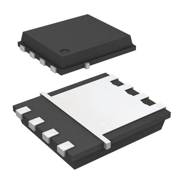
ICGOO电子元器件商城为您提供PHB21N06LT,118由NXP Semiconductors设计生产,在icgoo商城现货销售,并且可以通过原厂、代理商等渠道进行代购。 PHB21N06LT,118价格参考¥8.43-¥14.31。NXP SemiconductorsPHB21N06LT,118封装/规格:晶体管 - FET,MOSFET - 单, 表面贴装 N 沟道 55V 19A(Tc) 56W(Tc) D2PAK。您可以下载PHB21N06LT,118参考资料、Datasheet数据手册功能说明书,资料中有PHB21N06LT,118 详细功能的应用电路图电压和使用方法及教程。
Nexperia USA Inc. 的 PHB21N06LT,118 是一款 N 沟道增强型 MOSFET,常用于以下应用场景:

1. 电源管理:适用于开关电源(SMPS)、DC-DC 转换器和电池充电器,因其低导通电阻和高效能,有助于提高能效并减少热量产生。

2. 电机控制:用于电动工具、风扇、电动车和工业电机驱动电路中,作为高效的开关元件。

3. 负载开关:在电源管理系统中作为负载开关,控制电源的通断,保护电路免受过载或短路影响。

4. 照明系统:应用于 LED 照明的驱动电路中,提供稳定的电流控制和高效能切换。

5. 汽车电子:由于其可靠性和耐用性,也适用于汽车中的辅助电机、灯光系统和车载电源系统。

6. 工业自动化:在工业控制系统中用于继电器替代、PLC 输出开关和传感器驱动电路。

该器件采用小型封装,适合空间受限的设计,同时具备良好的热稳定性和耐用性,适合中高功率开关应用。
| 参数 | 数值 |
| 产品目录 | |
| 描述 | MOSFET N-CH 55V 19A D2PAK |
| 产品分类 | FET - 单 |
| FET功能 | 逻辑电平门 |
| FET类型 | MOSFET N 通道,金属氧化物 |
| 品牌 | NXP Semiconductors |
| 数据手册 | |
| 产品图片 |
|
| 产品型号 | PHB21N06LT,118 |
| PCN组件/产地 | |
| rohs | 无铅 / 符合限制有害物质指令(RoHS)规范要求 |
| 产品系列 | TrenchMOS™ |
| 不同Id时的Vgs(th)(最大值) | 2V @ 1mA |
| 不同Vds时的输入电容(Ciss) | 650pF @ 25V |
| 不同Vgs时的栅极电荷(Qg) | 9.4nC @ 5V |
| 不同 Id、Vgs时的 RdsOn(最大值) | 70 毫欧 @ 10A,10V |
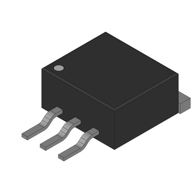
| 供应商器件封装 | D2PAK |
| 其它名称 | 568-5939-2 |
| 功率-最大值 | 56W |
| 包装 | 带卷 (TR) |
| 安装类型 | 表面贴装 |
| 封装/外壳 | TO-263-3,D²Pak(2 引线+接片),TO-263AB |
| 标准包装 | 800 |
| 漏源极电压(Vdss) | 55V |
| 电流-连续漏极(Id)(25°C时) | 19A (Tc) |


- 商务部:美国ITC正式对集成电路等产品启动337调查
- 曝三星4nm工艺存在良率问题 高通将骁龙8 Gen1或转产台积电
- 太阳诱电将投资9.5亿元在常州建新厂生产MLCC 预计2023年完工
- 英特尔发布欧洲新工厂建设计划 深化IDM 2.0 战略
- 台积电先进制程称霸业界 有大客户加持明年业绩稳了
- 达到5530亿美元!SIA预计今年全球半导体销售额将创下新高
- 英特尔拟将自动驾驶子公司Mobileye上市 估值或超500亿美元
- 三星加码芯片和SET,合并消费电子和移动部门,撤换高东真等 CEO
- 三星电子宣布重大人事变动 还合并消费电子和移动部门
- 海关总署:前11个月进口集成电路产品价值2.52万亿元 增长14.8%


PDF Datasheet 数据手册内容提取
Important notice Dear Customer, On 7 February 2017 the former NXP Standard Product business became a new company with the tradename Nexperia. Nexperia is an industry leading supplier of Discrete, Logic and PowerMOS semiconductors with its focus on the automotive, industrial, computing, consumer and wearable application markets In data sheets and application notes which still contain NXP or Philips Semiconductors references, use the references to Nexperia, as shown below. Instead of http://www.nxp.com, http://www.philips.com/ or http://www.semiconductors.philips.com/, use http://www.nexperia.com Instead of sales.addresses@www.nxp.com or sales.addresses@www.semiconductors.philips.com, use salesaddresses@nexperia.com (email) Replace the copyright notice at the bottom of each page or elsewhere in the document, depending on the version, as shown below: - © NXP N.V. (year). All rights reserved or © Koninklijke Philips Electronics N.V. (year). All rights reserved Should be replaced with: - © Nexperia B.V. (year). All rights reserved. If you have any questions related to the data sheet, please contact our nearest sales office via e-mail or telephone (details via salesaddresses@nexperia.com). Thank you for your cooperation and understanding, Kind regards, Team Nexperia
Philips Semiconductors Product specification N-channel TrenchMOS(cid:212) transistor PHP21N06LT, PHB21N06LT Logic level FET PHD21N06LT FEATURES SYMBOL QUICK REFERENCE DATA • ’Trench’ technology d VDSS = 55 V • Low on-state resistance • Fast switching I = 19 A D • Logic level compatible R £ 75 mW (V = 5 V) g DS(ON) GS R £ 70 mW (V = 10 V) DS(ON) GS s GENERAL DESCRIPTION N-channelenhancementmode,logiclevel,field-effectpowertransistorinaplasticenvelopeusing’trench’technology. Applications:- •d.c.tod.c.converters •switchedmodepowersupplies ThePHP21N06LTissuppliedintheSOT78(TO220AB)conventionalleadedpackage. ThePHB21N06LTissuppliedintheSOT404(D2PAK)surfacemountingpackage. ThePHD21N06LTissuppliedintheSOT428(DPAK)surfacemountingpackage. PINNING SOT78 (TO220AB) SOT404 (D2PAK) SOT428 (DPAK) PIN DESCRIPTION tab tab tab 1 gate 2 drain 1 2 2 3 source 123 1 3 1 3 tab drain LIMITING VALUES Limiting values in accordance with the Absolute Maximum System (IEC 134) SYMBOL PARAMETER CONDITIONS MIN. MAX. UNIT V Drain-source voltage T = 25 ˚C to 175˚C - 55 V DSS j V Drain-gate voltage T = 25 ˚C to 175˚C; R = 20 kW - 55 V DGR j GS V Gate-source voltage - – 15 V GS V Pulsed gate-source voltage T £ 150˚C - – 20 V GSM j I Continuous drain current T = 25 ˚C - 19 A D mb T = 100 ˚C - 13 A mb I Pulsed drain current T = 25 ˚C - 76 A DM mb P Total power dissipation T = 25 ˚C - 56 W D mb T, T Operating junction and - 55 175 ˚C j stg storage temperature 1 It is not possible to make connection to pin:2 of the SOT404 or SOT428 packages. August 1999 1 Rev 1.500
Philips Semiconductors Product specification N-channel TrenchMOS(cid:212) transistor PHP21N06LT, PHB21N06LT Logic level FET PHD21N06LT AVALANCHE ENERGY LIMITING VALUES Limiting values in accordance with the Absolute Maximum System (IEC 134) SYMBOL PARAMETER CONDITIONS MIN. MAX. UNIT E Non-repetitive avalanche Unclamped inductive load, I = 9.7 A; - 34 mJ AS AS energy t = 100 m s; T prior to avalanche = 25˚C; p j V £ 25 V; R = 50 W ; V = 5 V; refer to DD GS GS fig:15 I Peak non-repetitive - 19 A AS avalanche current THERMAL RESISTANCES SYMBOL PARAMETER CONDITIONS TYP. MAX. UNIT R Thermal resistance junction - 2.7 K/W th j-mb to mounting base R Thermal resistance junction SOT78 package, in free air 60 - K/W th j-a to ambient SOT428 and SOT404 package, pcb 50 - K/W mounted, minimum footprint ELECTRICAL CHARACTERISTICS T= 25˚C unless otherwise specified j SYMBOL PARAMETER CONDITIONS MIN. TYP. MAX. UNIT V Drain-source breakdown V = 0 V; I = 0.25 mA; 55 - - V (BR)DSS GS D voltage T = -55˚C 50 - - V j V Gate threshold voltage V = V ; I = 1 mA 1.0 1.5 2.0 V GS(TO) DS GS D T = 175˚C 0.5 - - V j T = -55˚C - - 2.3 V j R Drain-source on-state V = 10 V; I = 10 A - 55 70 mW DS(ON) GS D resistance V = 5 V; I = 10 A - 60 75 mW GS D T = 175˚C - - 158 mW j g Forward transconductance V = 25 V; I = 10 A 5 13 - S fs DS D I Gate source leakage current V = – 5 V; V = 0 V - 10 100 nA GSS GS DS I Zero gate voltage drain V = 55 V; V = 0 V; - 0.05 10 m A DSS DS GS current T = 175˚C - - 500 m A j Q Total gate charge I = 20 A; V = 44 V; V = 5 V - 9.4 - nC g(tot) D DD GS Q Gate-source charge - 2.2 - nC gs Q Gate-drain (Miller) charge - 5.4 - nC gd t Turn-on delay time V = 30 V; R = 1.2 W ; - 7 15 ns d on DD D t Turn-on rise time R = 10 W ; V = 5 V - 88 120 ns r G GS t Turn-off delay time Resistive load - 25 40 ns d off t Turn-off fall time - 25 45 ns f L Internal drain inductance Measured from tab to centre of die - 3.5 - nH d L Internal drain inductance Measured from drain lead to centre of die - 4.5 - nH d (SOT78 package only) L Internal source inductance Measured from source lead to source - 7.5 - nH s bond pad C Input capacitance V = 0 V; V = 25 V; f = 1 MHz - 466 650 pF iss GS DS C Output capacitance - 95 135 pF oss C Feedback capacitance - 71 85 pF rss August 1999 2 Rev 1.500
Philips Semiconductors Product specification N-channel TrenchMOS(cid:212) transistor PHP21N06LT, PHB21N06LT Logic level FET PHD21N06LT REVERSE DIODE LIMITING VALUES AND CHARACTERISTICS T = 25˚C unless otherwise specified j SYMBOL PARAMETER CONDITIONS MIN. TYP. MAX. UNIT I Continuous source current - - 19 A S (body diode) I Pulsed source current (body - - 76 A SM diode) V Diode forward voltage I = 20 A; V = 0 V - 1.2 1.5 V SD F GS t Reverse recovery time I = 20 A; -dI /dt = 100 A/m s; - 43 - ns rr F F Q Reverse recovery charge V = 0 V; V = 30 V - 94 - nC rr GS R Normalised Power Derating, PD (%) 100 Peak Pulsed Drain Current, IDM (A) 100 RDS(on) = VDS/ ID 90 tp = 10 us 80 70 10 60 100 us 50 1 ms 40 D.C. 10 ms 1 30 100 ms 20 10 0 0.1 0 25 50 75 100 125 150 175 1 10 100 Mounting Base temperature, Tmb (C) Drain-Source Voltage, VDS (V) Fig.1. Normalised power dissipation. Fig.3. Safe operating area. T = 25 ˚C PD% = 100(cid:215)P/P = f(T ) I & I = f(V ); I single pulse; mpbarameter t D D 25 ˚C mb D DM DS DM p Transient thermal impedance, Zth j-mb (K/W) Normalised Current Derating, ID (%) 10 100 90 D = 0.5 80 70 1 0.2 60 0.1 50 0.05 40 0.1 0.02 PD tp D = tp/T 30 single pulse 20 10 T 0 0.01 0 25 50 75 100 125 150 175 1E-06 1E-05 1E-04 1E-03 1E-02 1E-01 1E+00 Mounting Base temperature, Tmb (C) Pulse width, tp (s) Fig.2. Normalised continuous drain current. Fig.4. Transient thermal impedance. ID% = 100(cid:215)I/I = f(T ); conditions: V ‡ 5 V Z = f(t); parameter D = t/T D D 25 ˚C mb GS th j-mb p August 1999 3 Rev 1.500
Philips Semiconductors Product specification N-channel TrenchMOS(cid:212) transistor PHP21N06LT, PHB21N06LT Logic level FET PHD21N06LT Drain Current, ID (A) Transconductance, gfs (S) 35 15 Tj = 25 C 14 VDS > ID X RDS(ON) Tj = 25 C 30 VGS = 10V 5 V 13 12 25 11 175 C 10 9 20 3.4 V 8 7 15 3.2 V 6 3 V 5 10 4 2.8 V 3 5 2.6 V 2 2.4 V 1 0 0 0 0.2 0.4 0.6 0.8 1 1.2 1.4 1.6 1.8 2 0 2 4 6 8 10 12 14 16 18 20 Drain-Source Voltage, VDS (V) Drain current, ID (A) Fig.5. Typical output characteristics, T = 25 ˚C. Fig.8. Typical transconductance, T = 25 ˚C. j j I = f(V ) g = f(I) D DS fs D Normalised On-state Resistance Drain-Source On Resistance, RDS(on) (Ohms) 0.3 2.4 2.6 V 2.8V Tj = 25 C 2.2 0.25 2 2.4 V 1.8 0.2 3 V 1.6 1.4 0.15 3.2 V 1.2 3.4 V 1 0.1 0.8 5 V 0.6 0.4 0.05 0.2 VGS = 10V 0 0 -60 -40 -20 0 20 40 60 80 100 120 140 160 180 0 5 10 15 20 25 30 35 Drain Current, ID (A) Junction temperature, Tj (C) Fig.6. Typical on-state resistance, T = 25 ˚C. Fig.9. Normalised drain-source on-state resistance. j R = f(I) R /R = f(T) DS(ON) D DS(ON) DS(ON)25 ˚C j Threshold Voltage, VGS(TO) (V) Drain current, ID (A) 2.25 20 18 VDS > ID X RDS(ON) 2 maximum 16 1.75 14 1.5 typical 12 1.25 10 minimum 1 8 0.75 6 0.5 4 175 C 2 Tj = 25 C 0.25 0 0 0 0.5 1 1.5 2 2.5 3 3.5 4 4.5 5 -60 -40 -20 0 20 40 60 80 100 120 140 160 180 Gate-source voltage, VGS (V) Junction Temperature, Tj (C) Fig.7. Typical transfer characteristics. Fig.10. Gate threshold voltage. I = f(V ) V = f(T); conditions: I = 1 mA; V = V D GS GS(TO) j D DS GS August 1999 4 Rev 1.500
Philips Semiconductors Product specification N-channel TrenchMOS(cid:212) transistor PHP21N06LT, PHB21N06LT Logic level FET PHD21N06LT 1.0E-01 Drain current, ID (A) Source-Drain Diode Current, IF (A) 30 VGS = 0 V 1.0E-02 25 20 1.0E-03 minimum typical 15 175 C 1.0E-04 Tj = 25 C maximum 10 1.0E-05 5 1.0E-06 0 0 0.1 0.2 0.3 0.4 0.5 0.6 0.7 0.8 0.9 1 1.1 1.2 1.3 1.4 1.5 0 0.5 1 1.5 2 2.5 3 Gate-source voltage, VGS (V) Source-Drain Voltage, VSDS (V) Fig.11. Sub-threshold drain current. Fig.14. Typical reverse diode current. I = f(V ; conditions: T = 25 ˚C; V = V I = f(V ); conditions: V = 0 V; parameter T D GS) j DS GS F SDS GS j Maximum Avalanche Current, IAS (A) Capacitances, Ciss, Coss, Crss (pF) 100 10000 10 25 C 1000 Ciss Coss 1 Tj prior to avalanche = 150 C 100 Crss 0.1 10 0.001 0.01 0.1 1 10 0.1 1 10 100 Drain-Source Voltage, VDS (V) Avalanche time, tAV (ms) Fig.12. Typical capacitances, C , C , C . Fig.15. Maximum permissible non-repetitive iss oss rss C = f(V ); conditions: V = 0 V; f = 1 MHz avalanche current (I ) versus avalanche time (t ); DS GS AS AV unclamped inductive load Gate-source voltage, VGS (V) 15 14 ID = 20A 13 Tj = 25 C 12 11 10 VDD = 11 V 9 8 VDD = 44 V 7 6 5 4 3 2 1 0 0 2 4 6 8 10 12 14 16 18 20 Gate charge, QG (nC) Fig.13. Typical turn-on gate-charge characteristics. V = f(Q) GS G August 1999 5 Rev 1.500
Philips Semiconductors Product specification N-channel TrenchMOS(cid:212) transistor PHP21N06LT, PHB21N06LT Logic level FET PHD21N06LT MECHANICAL DATA Plastic single-ended package; heatsink mounted; 1 mounting hole; 3-lead TO-220 SOT78 E A P A1 q D1 D L2(1) L1 Q b1 L 1 2 3 b c e e 0 5 10 mm scale DIMENSIONS (mm are the original dimensions) (1) UNIT A A1 b b1 c D D1 E e L L1 L2 P q Q max. mm 4.5 1.39 0.9 1.3 0.7 15.8 6.4 10.3 2.54 15.0 3.30 3.0 3.8 3.0 2.6 4.1 1.27 0.7 1.0 0.4 15.2 5.9 9.7 13.5 2.79 3.6 2.7 2.2 Note 1. Terminals in this zone are not tinned. OUTLINE REFERENCES EUROPEAN ISSUE DATE VERSION IEC JEDEC EIAJ PROJECTION SOT78 TO-220 97-06-11 Fig.16. SOT78 (TO220AB); pin 2 connected to mounting base (Net mass:2g) Notes 1. This product is supplied in anti-static packaging. The gate-source input must be protected against static discharge during transport or handling. 2. Refer to mounting instructions for SOT78 (TO220AB) package. 3. Epoxy meets UL94 V0 at 1/8". August 1999 6 Rev 1.500
Philips Semiconductors Product specification N-channel TrenchMOS(cid:212) transistor PHP21N06LT, PHB21N06LT Logic level FET PHD21N06LT MECHANICAL DATA Plastic single-ended surface mounted package (Philips version of D2-PAK); 3 leads (one lead cropped) SOT404 A E A1 D1 mounting base D HD 2 Lp 1 3 b c e e Q 0 2.5 5 mm scale DIMENSIONS (mm are the original dimensions) UNIT A A1 b c mDax. D1 E e Lp HD Q mm 4.50 1.40 0.85 0.64 11 1.60 10.30 2.54 2.90 15.40 2.60 4.10 1.27 0.60 0.46 1.20 9.70 2.10 14.80 2.20 VOEURTSLIIONEN IEC JEDEC REFERENCES EIAJ PERUORJOEPCETAIONN ISSUE DATE SOT404 9989--1026--1245 Fig.17. SOT404 surface mounting package. Centre pin connected to mounting base. Notes 1. This product is supplied in anti-static packaging. The gate-source input must be protected against static discharge during transport or handling. 2. Refer to SMD Footprint Design and Soldering Guidelines, Data Handbook SC18. 3. Epoxy meets UL94 V0 at 1/8". August 1999 7 Rev 1.500
Philips Semiconductors Product specification N-channel TrenchMOS(cid:212) transistor PHP21N06LT, PHB21N06LT Logic level FET PHD21N06LT MOUNTING INSTRUCTIONS Dimensions in mm 11.5 9.0 17.5 2.0 3.8 5.08 Fig.18. SOT404 : soldering pattern for surface mounting. August 1999 8 Rev 1.500
Philips Semiconductors Product specification N-channel TrenchMOS(cid:212) transistor PHP21N06LT, PHB21N06LT Logic level FET PHD21N06LT MECHANICAL DATA Plastic single-ended surface mounted package (Philips version of D-PAK); 3 leads (one lead cropped) SOT428 seating plane y A E A A2 b2 A1 D1 mounting base E1 D HE L2 2 L L1 1 3 b1 b wM A c e e1 0 10 20 mm scale DIMENSIONS (mm are the original dimensions) UNIT mAax. A1(1) A2 b mba1x. b2 c mDax. mDa1x. mEax. mEi1n. e e1 mHaEx. L mLi1n. L2 w myax. mm 2.38 0.65 0.89 0.89 1.1 5.36 0.4 6.22 4.81 6.73 4.0 2.285 4.57 10.4 2.95 0.5 0.7 0.2 0.2 2.22 0.45 0.71 0.71 0.9 5.26 0.2 5.98 4.45 6.47 9.6 2.55 0.5 Note 1. Measured from heatsink back to lead. VOEURTSLIIONEN IEC JEDEC REFERENCES EIAJ PERUORJOEPCETAIONN ISSUE DATE SOT428 98-04-07 Fig.19. SOT428 surface mounting package. Centre pin connected to mounting base. Notes 1. This product is supplied in anti-static packaging. The gate-source input must be protected against static discharge during transport or handling. 2. Refer to SMD Footprint Design and Soldering Guidelines, Data Handbook SC18. 3. Epoxy meets UL94 V0 at 1/8". MOUNTING INSTRUCTIONS August 1999 9 Rev 1.500
Philips Semiconductors Product specification N-channel TrenchMOS(cid:212) transistor PHP21N06LT, PHB21N06LT Logic level FET PHD21N06LT Dimensions in mm 7.0 7.0 2.15 1.5 2.5 4.57 Fig.20. SOT428 : soldering pattern for surface mounting. August 1999 10 Rev 1.500
Philips Semiconductors Product specification N-channel TrenchMOS(cid:212) transistor PHP21N06LT, PHB21N06LT Logic level FET PHD21N06LT DEFINITIONS Data sheet status Objective specification This data sheet contains target or goal specifications for product development. Preliminary specification This data sheet contains preliminary data; supplementary data may be published later. Product specification This data sheet contains final product specifications. Limiting values Limiting values are given in accordance with the Absolute Maximum Rating System (IEC 134). Stress above one or more of the limiting values may cause permanent damage to the device. These are stress ratings only and operation of the device at these or at any other conditions above those given in the Characteristics sections of this specification is not implied. Exposure to limiting values for extended periods may affect device reliability. Application information Where application information is given, it is advisory and does not form part of the specification. (cid:211) Philips Electronics N.V. 1999 All rights are reserved. Reproduction in whole or in part is prohibited without the prior written consent of the copyright owner. The information presented in this document does not form part of any quotation or contract, it is believed to be accurate and reliable and may be changed without notice. No liability will be accepted by the publisher for any consequence of its use. Publication thereof does not convey nor imply any license under patent or other industrial or intellectual property rights. LIFE SUPPORT APPLICATIONS These products are not designed for use in life support appliances, devices or systems where malfunction of these products can be reasonably expected to result in personal injury. Philips customers using or selling these products for use in such applications do so at their own risk and agree to fully indemnify Philips for any damages resulting from such improper use or sale. August 1999 11 Rev 1.500