ICGOO在线商城 > 分立半导体产品 > 晶体管 - FET,MOSFET - 单 > STB42N65M5
 Datasheet下载
- 型号: STB42N65M5
- 制造商: STMicroelectronics
- 库位|库存: xxxx|xxxx
- 要求:
| 数量阶梯 | 香港交货 | 国内含税 |
| +xxxx | $xxxx | ¥xxxx |
查看当月历史价格
查看今年历史价格
STB42N65M5产品简介:
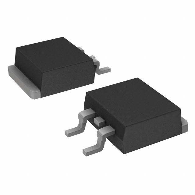
ICGOO电子元器件商城为您提供STB42N65M5由STMicroelectronics设计生产,在icgoo商城现货销售,并且可以通过原厂、代理商等渠道进行代购。 STB42N65M5价格参考¥61.99-¥74.43。STMicroelectronicsSTB42N65M5封装/规格:晶体管 - FET,MOSFET - 单, 表面贴装 N 沟道 650V 33A(Tc) 190W(Tc) D2PAK。您可以下载STB42N65M5参考资料、Datasheet数据手册功能说明书,资料中有STB42N65M5 详细功能的应用电路图电压和使用方法及教程。
STB42N65M5是由STMicroelectronics(意法半导体)生产的单通道MOSFET(金属氧化物场效应晶体管)。这款MOSFET属于N沟道增强型功率MOSFET,具有高耐压和低导通电阻的特点。其应用场景广泛,适用于各种需要高效开关和功率管理的电路设计。

 主要应用场景

1. 电源管理系统:
   - STB42N65M5适用于开关电源、DC-DC转换器等电源管理系统。它能够高效地进行电压转换和电流控制,确保系统稳定运行。
   - 在不间断电源(UPS)中,该MOSFET可以用于电池充电和放电管理,提供可靠的电力保护。

2. 电机驱动与控制:
   - 该器件可用于驱动直流电机、步进电机和无刷直流电机(BLDC)。在电机驱动应用中,MOSFET作为开关元件,通过快速切换实现精确的速度和扭矩控制。
   - 在工业自动化设备中,如伺服驱动器、机器人控制系统等,STB42N65M5可以提供高效的功率传输和控制。

3. 逆变器与变频器:
   - 在太阳能逆变器、风力发电逆变器等可再生能源系统中,STB42N65M5可以用于将直流电转换为交流电,提高能源转换效率。
   - 变频器中,该MOSFET用于调节电动机的速度和转矩,广泛应用于空调、洗衣机等家电产品中。

4. 汽车电子:
   - 在汽车电子领域,STB42N65M5可用于车载充电器、LED照明系统、电动助力转向系统(EPS)、制动系统等。其高可靠性和耐高压特性使其适合严苛的汽车环境。
   - 新能源汽车中的电池管理系统(BMS)也广泛应用该MOSFET,以确保电池的安全和高效使用。

5. 消费电子:
   - 在笔记本电脑、平板电脑等便携式设备中,STB42N65M5可用于电源管理模块,提供高效的电源转换和保护功能。
   - 智能家居设备如智能灯泡、智能插座等也可以使用该MOSFET来实现节能和远程控制。

总之,STB42N65M5凭借其出色的电气性能和可靠性,在多个行业和应用场景中发挥着重要作用。
| 参数 | 数值 |
| 产品目录 | |
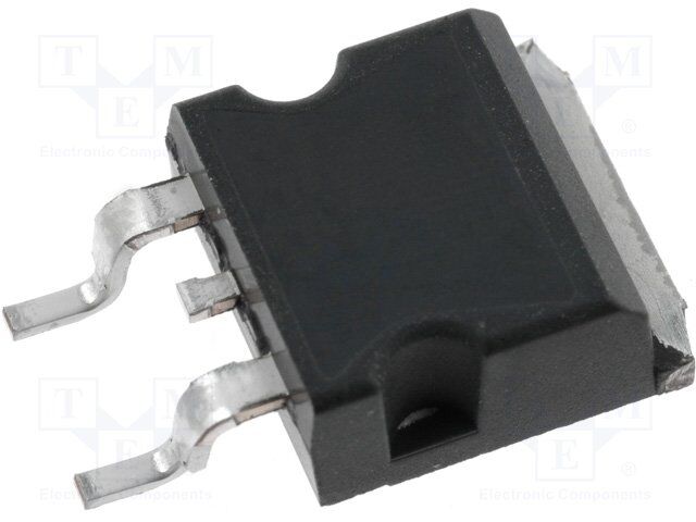
| 描述 | MOSFET N-CH 650V 33A D2PAK |
| 产品分类 | FET - 单 |
| FET功能 | 标准 |
| FET类型 | MOSFET N 通道,金属氧化物 |
| 品牌 | STMicroelectronics |
| 数据手册 | |
| 产品图片 |
|
| 产品型号 | STB42N65M5 |
| rohs | 无铅 / 符合限制有害物质指令(RoHS)规范要求 |
| 产品系列 | MDmesh™ V |
| 不同Id时的Vgs(th)(最大值) | 5V @ 250µA |
| 不同Vds时的输入电容(Ciss) | 4650pF @ 100V |
| 不同Vgs时的栅极电荷(Qg) | 100nC @ 10V |
| 不同 Id、Vgs时的 RdsOn(最大值) | 79 毫欧 @ 16.5A,10V |
| 产品培训模块 | http://www.digikey.cn/PTM/IndividualPTM.page?site=cn&lang=zhs&ptm=21007 |
| 产品目录页面 | |
| 供应商器件封装 | D2PAK |
| 其它名称 | 497-8769-2 |
| 其它有关文件 | http://www.st.com/web/catalog/sense_power/FM100/CL824/SC1167/PF219966?referrer=70071840 |
| 功率-最大值 | 190W |
| 包装 | 带卷 (TR) |
| 安装类型 | 表面贴装 |
| 封装/外壳 | TO-263-3,D²Pak(2 引线+接片),TO-263AB |
| 工具箱 | /product-detail/zh/497-8012-KIT/497-8012-KIT-ND/2340669 |
| 标准包装 | 1,000 |
| 漏源极电压(Vdss) | 650V |
| 特色产品 | http://www.digikey.com/cn/zh/ph/st/mdmeshv.html |
| 电流-连续漏极(Id)(25°C时) | 33A (Tc) |


- 商务部:美国ITC正式对集成电路等产品启动337调查
- 曝三星4nm工艺存在良率问题 高通将骁龙8 Gen1或转产台积电
- 太阳诱电将投资9.5亿元在常州建新厂生产MLCC 预计2023年完工
- 英特尔发布欧洲新工厂建设计划 深化IDM 2.0 战略
- 台积电先进制程称霸业界 有大客户加持明年业绩稳了
- 达到5530亿美元!SIA预计今年全球半导体销售额将创下新高
- 英特尔拟将自动驾驶子公司Mobileye上市 估值或超500亿美元
- 三星加码芯片和SET,合并消费电子和移动部门,撤换高东真等 CEO
- 三星电子宣布重大人事变动 还合并消费电子和移动部门
- 海关总署:前11个月进口集成电路产品价值2.52万亿元 增长14.8%


PDF Datasheet 数据手册内容提取
STB42N65M5, STF42N65M5, STI42N65M5 STP42N65M5, STW42N65M5 Datasheet N-channel 650 V, 70 mΩ typ., 33 A, MDmesh M5 Power MOSFETs in D²PAK, TO-220FP, I²PAK, TO-220 and TO-247 packages Features TAB Order codes VDS @ TJmax RDS(on) max. ID Package 3 1 23 STB42N65M5 D²PAK D2 PAK 1 TAB TO-220FP STF42N65M5 TO-220FP STI42N65M5 710 V 79 mΩ 33 A I²PAK STP42N65M5 TO-220 I2PAK 123 STW42N65M5 TO-247 TAB • Extremely low R DS(on) • Low gate charge and input capacitance 123 123 • Excellent switching performance TO-220 TO-247 • 100% avalanche tested D(2, TAB) Applications • Switching applications G(1) Description These devices are N-channel Power MOSFETs based on the MDmesh M5 innovative vertical process technology combined with the well-known PowerMESH horizontal S(3) layout. The resulting products offer extremely low on-resistance, making them AM01475v1_noZen particularly suitable for applications requiring high power and superior efficiency. Product status STB42N65M5 STF42N65M5 STI42N65M5 STP42N65M5 STW42N65M5 DS6033 - Rev 4 - May 2019 www.st.com For further information contact your local STMicroelectronics sales office.
STB42N65M5, STF42N65M5, STI42N65M5, STP42N65M5, STW42N65M5 Electrical ratings 1 Electrical ratings Table 1. Absolute maximum ratings Value Symbol Parameter Unit D²PAK, I²PAK, TO-220FP TO-220, TO-247 VGS Gate-source voltage ±25 V Drain current (continuous) at TC = 25 °C 33 33(1) A ID Drain current (continuous) at TC = 100 °C 20.8 20.8 (1) A IDM(2) Drain current (pulsed) 132 132 A PTOT Total power dissipation at TC = 25 °C 190 40 W dv/dt(3) Peak diode recovery voltage slope 15 V/ns Insulation withstand voltage (RMS) from all three VISO leads to external heat sink (t = 1 s; TC = 25 °C) 2500 V Tj Operating junction temperature range -55 to 150 °C Tstg Storage temperature range 1. Limited by maximum junction temperature. 2. Pulse width limited by safe operating area. 3. ISD ≤ 33 A, di/dt ≤ 400 A/μs, VDD = 400 V, VDS(peak) < V(BR)DSS. Table 2. Thermal data Value Symbol Parameter Unit D²PAK I²PAK TO-220 TO-247 TO-220FP Thermal resistance Rthj-case junction-case 0.66 3.1 °C/W Thermal resistance Rthj-amb junction-ambient 62.5 50 62.5 °C/W Thermal resistance Rthj-pcb (1) junction-pcb 30 °C/W 1. When mounted on an 1 inch² FR-4, 2 Oz copper board. Table 3. Avalanche characteristics Symbol Parameter Value Unit Avalanche current, repetitive or non-repetitive IAR (pulse width limited by Tjmax) 11 A Single pulse avalanche energy EAS 950 mJ (starting Tj = 25 °C, ID = IAR, VDD = 50 V) DS6033 - Rev 4 page 2/25
STB42N65M5, STF42N65M5, STI42N65M5, STP42N65M5, STW42N65M5 Electrical characteristics 2 Electrical characteristics (T = 25 °C unless otherwise specified) CASE Table 4. On/off states Symbol Parameter Test conditions Min. Typ. Max. Unit V(BR)DSS Drain-source breakdown voltage ID = 1 mA, VGS = 0 V 650 V VGS = 0 V, VDS = 650 V 1 µA IDSS Zero gate voltage drain current VGS = 0 V, VDS = 650 V, 100 µA TC = 125 °C (1) IGSS Gate body leakage current VGS = ±25 V, VDS= 0 V 100 nA VGS(th) Gate threshold voltage VDS = VGS, ID = 250 µA 3 4 5 V RDS(on) Static drain-source on- resistance VGS = 10 V, ID = 16.5 A 70 79 mΩ 1. Defined by design, not subject to production test. Table 5. Dynamic Symbol Parameter Test conditions Min. Typ. Max. Unit Ciss Input capacitance 4650 VDS = 100 V, f = 1 MHz, Coss Output capacitance - 110 - pF VGS = 0 V Crss Reverse transfer capacitance 3.2 Equivalent capacitance time Co(tr) (1) related - 100 - VDS = 0 to 520 V, VGS = 0 V pF Equivalent capacitance Co(er) (2) 285 - energy related Rg Gate input resistance f = 1 MHz, ID = 0 A - 1.1 - Ω Qg Total gate charge VDD = 520 V, ID = 33 A, 98 - Qgs Gate-source charge VGS = 0 to 10 V - 28 nC (see Figure 20. Test circuit for gate - Qgd Gate-drain charge charge behavior) 39 1. Co(tr) is a constant capacitance value that gives the same charging time as Coss while VDS is rising from 0 to 80% VDSS. 2. Co(er) is a constant capacitance value that gives the same stored energy as Coss while VDS is rising from 0 to 80% VDSS. Table 6. Switching times Symbol Parameter Test conditions Min. Typ. Max. Unit td(v) Voltage delay time VDD = 400 V, ID = 20 A, 52 tr(v) Voltage rise time RG = 4.7 Ω, VGS = 10 V 8.4 tf(i) Current fall time (see Figure 21. Test circuit for - 8.7 - ns inductive load switching and diode recovery times and tc(off) Crossing time Figure 24. Switching time 14 waveform) DS6033 - Rev 4 page 3/25
STB42N65M5, STF42N65M5, STI42N65M5, STP42N65M5, STW42N65M5 Electrical characteristics Table 7. Source-drain diode Symbol Parameter Test conditions Min. Typ. Max. Unit ISD Source-drain current 33 - A ISDM(1) Source-drain current (pulsed) 132 VSD(2) Forward on voltage ISD = 33 A, VGS = 0 V - 1.5 V trr Reverse recovery time ISD = 33 A, di/dt = 100 A/µs 400 ns Qrr Reverse recovery charge VDD = 100 V 7 μC - (see Figure 21. Test circuit for IRRM Reverse recovery current inductive load switching and diode 35 A recovery times) trr Reverse recovery time ISD = 33 A, di/dt = 100 A/µs 532 ns Qrr Reverse recovery charge VDD = 100 V, Tj = 150 °C 10 μC - (see Figure 21. Test circuit for IRRM Reverse recovery current inductive load switching and diode 38 A recovery times) 1. Pulse width limited by safe operating area. 2. Pulsed: pulse duration = 300 μs, duty cycle 1.5%. DS6033 - Rev 4 page 4/25
STB42N65M5, STF42N65M5, STI42N65M5, STP42N65M5, STW42N65M5 Electrical characteristics (curves) 2.1 Electrical characteristics (curves) Figure 1. Safe operating area for D²PAK, I²PAK, TO-220 Figure 2. Thermal impedance for D²PAK, I²PAK, TO-220 ID AM01565v1 (A) 100 10 OperLiatimiotne id n btyh ism aarx eaR iDsS(on) 11100m0µµsss 1 10ms 0.1 0.1 1 10 100 VDS(V) Figure 3. Safe operating area for TO-247 Figure 4. Thermal impedance for TO-247 ID AM03246v1 (A) 100 10 OperLiatimiotne id n btyh ism aarx eaR iDsS(on) 11100m0µµsss 10ms 1 0.1 0.1 1 10 100 VDS(V) Figure 5. Safe operating area for TO-220FP Figure 6. Thermal impedance for TO-220FP ID AM01566v1 K GC20521 (A) δ =0.5 100 0.2 10 OpeLriatmiitoen di nb ty hims aaxr eRa DiSs(on) 11000µµss 10-1 0.1 0.002.05 1 1ms 0.01 0.1 10ms 10-2 Single pulse Zδt h= =t pK /* ƬR thJ-c 0.01 10-3 tpƬ 0.1 1 10 100 VDS(V) 10-4 10-3 10-2 10-1 10-0 tp(s) DS6033 - Rev 4 page 5/25
STB42N65M5, STF42N65M5, STI42N65M5, STP42N65M5, STW42N65M5 Electrical characteristics (curves) Figure 7. Output characteristics Figure 8. Transfer characteristics ID AM01589V1 ID AM01590V1 (A) (A) 100 VGS = 9, 10 V 100 VDS = 15 V VGS =8 V 80 80 60 60 40 VGS =7 V 40 20 20 0 VGS =6 V 0 0 2 4 6 8 10 12 14 VDS (V) 4 5 6 7 8 9 VGS (V) Figure 9. Gate charge vs gate-source voltage Figure 10. Static drain-source on-resistance VDS AM01569V1VGS RDS(on) AM01568V1 (V) (V) (mΩ) 600 VDD = 520 V 12 76 VGS = 10 V ID = 33 A 500 VDS 10 74 400 8 72 300 6 70 200 4 68 100 2 66 0 0 64 0 20 40 60 80 100 120 Qg (nC) 0 5 10 15 20 25 30 ID (A) Figure 11. Capacitance variations Figure 12. Output capacitance stored energy C AM01570v1 Eoss AM03231v1 (pF) (µJ) 10000 16 Ciss 14 1000 12 10 100 Coss 8 6 10 4 Crss 2 1 0 1 10 100 VDS(V) 0 100 200 300 400 500 600 VDS(V) DS6033 - Rev 4 page 6/25
STB42N65M5, STF42N65M5, STI42N65M5, STP42N65M5, STW42N65M5 Electrical characteristics (curves) Figure 13. Normalized gate threshold voltage vs Figure 14. Normalized on-resistance vs temperature temperature VGS(th) AM01571V1 (nRoDrSm(o.n)) AM01573V1 (norm.) 1.1 ID = 250 μA 2.5 VGS = 10 V 2.0 1.0 1.5 0.9 1.0 0.8 0.5 0.7 0.0 0.6 -75 -25 25 75 125 TJ (°C) -75 -25 25 75 125 TJ (°C) Figure 15. Source-drain diode forward characteristics Figure 16. Normalized V(BR)DSS vs temperature VSD AM01574v1 V(BR)DSS AM01572V1 (V) (norm.) 1.0 TJ=-25°C 1.12 0.9 ID = 1 mA 1.08 0.8 0.7 1.04 0.6 TJ=25°C 1.00 0.5 TJ=150°C 0.96 0.4 0.3 0.92 0.2 0.88 0 5 10 15 20 25 30 ISD(A) -75 -25 25 75 125 TJ (°C) Figure 17. Switching energy vs gate resistance E AM01575v1 (µJ) Eon ID=20A 600 VDD=400V L=50µH 500 400 300 Eoff 200 100 0 0 5 10 15 20 25 30 35 40 45 RG(W) Note: E including reverse recovery of a SiC diode. on DS6033 - Rev 4 page 7/25
STB42N65M5, STF42N65M5, STI42N65M5, STP42N65M5, STW42N65M5 Test circuits 3 Test circuits Figure 19. Test circuit for resistive load switching times Figure 20. Test circuit for gate charge behavior VDD 12 V 47 kΩ 1 kΩ 100 nF RL 2200 3.3 + μF μF VDD VD VGS IG= CONST 100 Ω D.U.T. VGS RG D.U.T. pulse width + 2.7 kΩ 2200 VG pulse width μF 47 kΩ 1 kΩ AM01468v1 AM01469v1 Figure 21. Test circuit for inductive load switching and Figure 22. Unclamped inductive load test circuit diode recovery times A A A L D fast 100 µH VD G D.U.T. diode 2200 3.3 25 Ω S B B B D µ3F.3 +1µ0F00 VDD ID +µF µF VDD G D.U.T. + RG S Vi D.U.T. _ pulse width AM01471v1 AM01470v1 Figure 23. Unclamped inductive waveform Figure 24. Switching time waveform V(BR)DSS Concept waveform for Inductive Load Turn-off Id VD 90%Vds 90%Id Tdelay--ooffff IDM Vgs 90%Vgs oonn ID Vgs(I(t)))) VDD VDD 10%Vds 10%Id Vds TTrriissee TTffaallll AM01472v1 Tcross--over AM05540v2 DS6033 - Rev 4 page 8/25
STB42N65M5, STF42N65M5, STI42N65M5, STP42N65M5, STW42N65M5 Package information 4 Package information In order to meet environmental requirements, ST offers these devices in different grades of ECOPACK packages, depending on their level of environmental compliance. ECOPACK specifications, grade definitions and product status are available at: www.st.com. ECOPACK is an ST trademark. DS6033 - Rev 4 page 9/25
STB42N65M5, STF42N65M5, STI42N65M5, STP42N65M5, STW42N65M5 D²PAK (TO-263) type A2 package information 4.1 D²PAK (TO-263) type A2 package information Figure 25. D²PAK (TO-263) type A2 package outline 0079457_A2_26 DS6033 - Rev 4 page 10/25
STB42N65M5, STF42N65M5, STI42N65M5, STP42N65M5, STW42N65M5 D²PAK (TO-263) type A2 package information Table 8. D²PAK (TO-263) type A2 package mechanical data mm Dim. Min. Typ. Max. A 4.40 4.60 A1 0.03 0.23 b 0.70 0.93 b2 1.14 1.70 c 0.45 0.60 c2 1.23 1.36 D 8.95 9.35 D1 7.50 7.75 8.00 D2 1.10 1.30 1.50 E 10.00 10.40 E1 8.70 8.90 9.10 E2 7.30 7.50 7.70 e 2.54 e1 4.88 5.28 H 15.00 15.85 J1 2.49 2.69 L 2.29 2.79 L1 1.27 1.40 L2 1.30 1.75 R 0.40 V2 0° 8° Figure 26. D²PAK (TO-263) recommended footprint (dimensions are in mm) Footprint DS6033 - Rev 4 page 11/25
STB42N65M5, STF42N65M5, STI42N65M5, STP42N65M5, STW42N65M5 D²PAK packing information 4.2 D²PAK packing information Figure 27. D²PAK tape outline DS6033 - Rev 4 page 12/25
STB42N65M5, STF42N65M5, STI42N65M5, STP42N65M5, STW42N65M5 D²PAK packing information Figure 28. D²PAK reel outline T 40mm min. access hole at slot location B D C N A Tape slot G measured in core for at hub Full radius tape start 2.5mm min.width AM06038v1 Table 9. D²PAK tape and reel mechanical data Tape Reel mm mm Dim. Dim. Min. Max. Min. Max. A0 10.5 10.7 A 330 B0 15.7 15.9 B 1.5 D 1.5 1.6 C 12.8 13.2 D1 1.59 1.61 D 20.2 E 1.65 1.85 G 24.4 26.4 F 11.4 11.6 N 100 K0 4.8 5.0 T 30.4 P0 3.9 4.1 P1 11.9 12.1 Base quantity 1000 P2 1.9 2.1 Bulk quantity 1000 R 50 T 0.25 0.35 W 23.7 24.3 DS6033 - Rev 4 page 13/25
STB42N65M5, STF42N65M5, STI42N65M5, STP42N65M5, STW42N65M5 TO-220FP package information 4.3 TO-220FP package information Figure 29. TO-220FP package outline 7012510_Rev_12_B DS6033 - Rev 4 page 14/25
STB42N65M5, STF42N65M5, STI42N65M5, STP42N65M5, STW42N65M5 TO-220FP package information Table 10. TO-220FP package mechanical data mm Dim. Min. Typ. Max. A 4.4 4.6 B 2.5 2.7 D 2.5 2.75 E 0.45 0.7 F 0.75 1 F1 1.15 1.70 F2 1.15 1.70 G 4.95 5.2 G1 2.4 2.7 H 10 10.4 L2 16 L3 28.6 30.6 L4 9.8 10.6 L5 2.9 3.6 L6 15.9 16.4 L7 9 9.3 Dia 3 3.2 DS6033 - Rev 4 page 15/25
STB42N65M5, STF42N65M5, STI42N65M5, STP42N65M5, STW42N65M5 I²PAK package information 4.4 I²PAK package information Figure 30. I²PAK package outline 0004982_Rev_H DS6033 - Rev 4 page 16/25
STB42N65M5, STF42N65M5, STI42N65M5, STP42N65M5, STW42N65M5 I²PAK package information Table 11. I²PAK package mechanical data mm Dim. Min. Typ. Max. A 4.40 - 4.60 A1 2.40 - 2.72 b 0.61 - 0.88 b1 1.14 - 1.70 c 0.49 - 0.70 c2 1.23 - 1.32 D 8.95 - 9.35 e 2.40 - 2.70 e1 4.95 - 5.15 E 10 - 10.40 L 13 - 14 L1 3.50 - 3.93 L2 1.27 - 1.40 DS6033 - Rev 4 page 17/25
STB42N65M5, STF42N65M5, STI42N65M5, STP42N65M5, STW42N65M5 TO-220 type A package information 4.5 TO-220 type A package information Figure 31. TO-220 type A package outline 0015988_typeA_Rev_22 DS6033 - Rev 4 page 18/25
STB42N65M5, STF42N65M5, STI42N65M5, STP42N65M5, STW42N65M5 TO-220 type A package information Table 12. TO-220 type A package mechanical data mm Dim. Min. Typ. Max. A 4.40 4.60 b 0.61 0.88 b1 1.14 1.55 c 0.48 0.70 D 15.25 15.75 D1 1.27 E 10.00 10.40 e 2.40 2.70 e1 4.95 5.15 F 1.23 1.32 H1 6.20 6.60 J1 2.40 2.72 L 13.00 14.00 L1 3.50 3.93 L20 16.40 L30 28.90 øP 3.75 3.85 Q 2.65 2.95 DS6033 - Rev 4 page 19/25
STB42N65M5, STF42N65M5, STI42N65M5, STP42N65M5, STW42N65M5 TO-247 package information 4.6 TO-247 package information Figure 32. TO-247 package outline 0075325_9 DS6033 - Rev 4 page 20/25
STB42N65M5, STF42N65M5, STI42N65M5, STP42N65M5, STW42N65M5 TO-247 package information Table 13. TO-247 package mechanical data mm Dim. Min. Typ. Max. A 4.85 5.15 A1 2.20 2.60 b 1.0 1.40 b1 2.0 2.40 b2 3.0 3.40 c 0.40 0.80 D 19.85 20.15 E 15.45 15.75 e 5.30 5.45 5.60 L 14.20 14.80 L1 3.70 4.30 L2 18.50 ØP 3.55 3.65 ØR 4.50 5.50 S 5.30 5.50 5.70 DS6033 - Rev 4 page 21/25
STB42N65M5, STF42N65M5, STI42N65M5, STP42N65M5, STW42N65M5 Ordering information 5 Ordering information Table 14. Order codes Order code Marking Package Packing STB42N65M5 D²PAK Tape and reel STF42N65M5 TO-220FP STI42N65M5 42N65M5 I²PAK Tube STP42N65M5 TO-220 STW42N65M5 TO-247 DS6033 - Rev 4 page 22/25
STB42N65M5, STF42N65M5, STI42N65M5, STP42N65M5, STW42N65M5 Revision history Table 15. Document revision history Date Version Changes 16-Jan-2009 1 First release. 15-May-2009 2 Updated figures 9, 10, 11 and 17 12-Jun-2009 3 Figure 15 has been updated Modified features and description on cover page. 02-May-2019 4 Updated Section 4 Package information. Minor text changes. DS6033 - Rev 4 page 23/25
STB42N65M5, STF42N65M5, STI42N65M5, STP42N65M5, STW42N65M5 Contents Contents 1 Electrical ratings ..................................................................2 2 Electrical characteristics...........................................................3 2.1 Electrical characteristics (curves) .................................................5 3 Test circuits .......................................................................8 4 Package information...............................................................9 4.1 D²PAK (TO-263) type A2 package information ......................................9 4.2 D²PAK packing information .....................................................11 4.3 TO-220FP package information .................................................13 4.4 I²PAK package information......................................................15 4.5 TO-220 type A package information..............................................17 4.6 TO-247 package information....................................................19 5 Ordering information .............................................................22 Revision history .......................................................................23 DS6033 - Rev 4 page 24/25
STB42N65M5, STF42N65M5, STI42N65M5, STP42N65M5, STW42N65M5 IMPORTANT NOTICE – PLEASE READ CAREFULLY STMicroelectronics NV and its subsidiaries (“ST”) reserve the right to make changes, corrections, enhancements, modifications, and improvements to ST products and/or to this document at any time without notice. Purchasers should obtain the latest relevant information on ST products before placing orders. ST products are sold pursuant to ST’s terms and conditions of sale in place at the time of order acknowledgement. Purchasers are solely responsible for the choice, selection, and use of ST products and ST assumes no liability for application assistance or the design of Purchasers’ products. No license, express or implied, to any intellectual property right is granted by ST herein. Resale of ST products with provisions different from the information set forth herein shall void any warranty granted by ST for such product. ST and the ST logo are trademarks of ST. For additional information about ST trademarks, please refer to www.st.com/trademarks. All other product or service names are the property of their respective owners. Information in this document supersedes and replaces information previously supplied in any prior versions of this document. © 2019 STMicroelectronics – All rights reserved DS6033 - Rev 4 page 25/25
Mouser Electronics Authorized Distributor Click to View Pricing, Inventory, Delivery & Lifecycle Information: S TMicroelectronics: STF42N65M5 STI42N65M5 STW42N65M5 STB42N65M5 STP42N65M5