ICGOO在线商城 > 分立半导体产品 > 晶体管 - FET,MOSFET - 单 > DMN3010LFG-7
 Datasheet下载
- 型号: DMN3010LFG-7
- 制造商: Diodes Inc.
- 库位|库存: xxxx|xxxx
- 要求:
| 数量阶梯 | 香港交货 | 国内含税 |
| +xxxx | $xxxx | ¥xxxx |
查看当月历史价格
查看今年历史价格
DMN3010LFG-7产品简介:
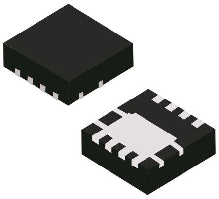
ICGOO电子元器件商城为您提供DMN3010LFG-7由Diodes Inc.设计生产,在icgoo商城现货销售,并且可以通过原厂、代理商等渠道进行代购。 DMN3010LFG-7价格参考。Diodes Inc.DMN3010LFG-7封装/规格:晶体管 - FET,MOSFET - 单, 表面贴装 N 沟道 30V 11A(Ta),30A(Tc) 900mW(Ta) PowerDI3333-8。您可以下载DMN3010LFG-7参考资料、Datasheet数据手册功能说明书,资料中有DMN3010LFG-7 详细功能的应用电路图电压和使用方法及教程。
DMN3010LFG-7 是由 Diodes Incorporated 生产的一款 N 通道增强型 MOSFET,属于晶体管 - FET、MOSFET - 单类别的产品。以下是其主要应用场景:

 1. 电源管理
   - 负载开关:该 MOSFET 可用于负载开关应用中,实现对电路的动态控制,保护下游电路免受过流或短路的影响。
   - DC-DC 转换器:适用于降压或升压 DC-DC 转换器中的开关元件,提供高效的功率转换。
   - 线性稳压器 (LDO):作为 LDO 的外部开关元件,帮助调节输出电压。

 2. 电池管理系统
   - 电池保护:用于锂电池或其他电池组的充放电保护电路中,防止过充、过放或短路。
   - 电池切换:在多电池系统中,用作电池切换开关,确保系统始终使用合适的电源。

 3. 消费电子
   - 便携式设备:如智能手机、平板电脑、笔记本电脑等,可用于音频放大器驱动、摄像头模块供电等场景。
   - USB 端口保护:在 USB 充电或数据传输端口中,用作过流保护和快速开关元件。

 4. 通信与网络设备
   - 信号调节:在通信设备中用于信号路径的开关或调节。
   - 热插拔保护:在网络交换机、路由器等设备中,防止热插拔时的电流冲击。

 5. 工业自动化
   - 电机驱动:用于小型直流电机的启停和速度控制。
   - 传感器接口:作为传感器信号的开关或放大电路的一部分。

 6. 汽车电子
   - 车载信息娱乐系统:用于音频功放、显示屏背光控制等。
   - 辅助功能控制:如车窗升降、座椅加热等低功率控制应用。

 特点支持:
- 低导通电阻 (Rds(on)):有助于降低功耗,提高效率。
- 小封装尺寸 (SOT363/SC-70):适合空间受限的应用。
- 高开关速度:适合高频开关应用。
- 良好的热性能:能够在较高环境温度下稳定工作。

综上所述,DMN3010LFG-7 凭借其低导通电阻、小封装和高性能,广泛应用于各种低功率、高效率需求的电子设备中。
| 参数 | 数值 |
| 产品目录 | |
| 描述 | MOSFET N-CH 30V 11A POWERDI |
| 产品分类 | FET - 单 |
| FET功能 | 逻辑电平门 |
| FET类型 | MOSFET N 通道,金属氧化物 |
| 品牌 | Diodes Incorporated |
| 数据手册 | |
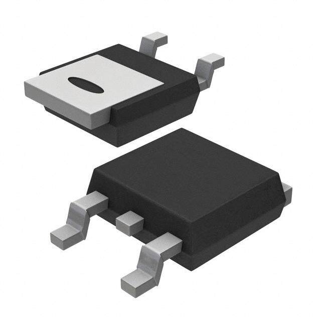
| 产品图片 |
|
| 产品型号 | DMN3010LFG-7 |
| rohs | 无铅 / 符合限制有害物质指令(RoHS)规范要求 |
| RoHS指令信息 | http://diodes.com/download/4349 |
| 产品系列 | - |
| 不同Id时的Vgs(th)(最大值) | 2.5V @ 250µA |
| 不同Vds时的输入电容(Ciss) | 2075pF @ 15V |
| 不同Vgs时的栅极电荷(Qg) | 37nC @ 10V |
| 不同 Id、Vgs时的 RdsOn(最大值) | 8.5 毫欧 @ 18A,10V |
| 供应商器件封装 | PowerDI3333-8 |
| 其它名称 | DMN3010LFG-7DIDKR |
| 功率-最大值 | 900mW |
| 包装 | Digi-Reel® |
| 安装类型 | 表面贴装 |
| 封装/外壳 | 8-PowerVDFN |
| 标准包装 | 1 |
| 漏源极电压(Vdss) | 30V |
| 电流-连续漏极(Id)(25°C时) | 11A (Ta), 30A (Tc) |


- 商务部:美国ITC正式对集成电路等产品启动337调查
- 曝三星4nm工艺存在良率问题 高通将骁龙8 Gen1或转产台积电
- 太阳诱电将投资9.5亿元在常州建新厂生产MLCC 预计2023年完工
- 英特尔发布欧洲新工厂建设计划 深化IDM 2.0 战略
- 台积电先进制程称霸业界 有大客户加持明年业绩稳了
- 达到5530亿美元!SIA预计今年全球半导体销售额将创下新高
- 英特尔拟将自动驾驶子公司Mobileye上市 估值或超500亿美元
- 三星加码芯片和SET,合并消费电子和移动部门,撤换高东真等 CEO
- 三星电子宣布重大人事变动 还合并消费电子和移动部门
- 海关总署:前11个月进口集成电路产品价值2.52万亿元 增长14.8%


PDF Datasheet 数据手册内容提取
DMN3010LFG N-CHANNEL ENHANCEMENT MODE MOSFET POWERDI® Product Summary Features ID Low RDS(ON) – ensures on state losses are minimized V(BR)DSS RDS(ON) TC = +25°C Small form factor thermally efficient package enables higher 8.5mΩ @ VGS = 10V 30A density end products 30V 10.5mΩ @ VGS = 4.5V 25A Occupies just 33% of the board area occupied by SO-8 enabling smaller end product Description 100% UIS (Avalanche) rated 100% Rg tested T This new generation MOSFET is designed to minimize the on-state Totally Lead-Free & Fully RoHS Compliant (Notes 1 & 2) C resistance (RDS(ON)) and yet maintain superior switching performance, Halogen and Antimony Free. “Green” Device (Note 3) U making it ideal for high-efficiency power management applications. Qualified to AEC-Q101 Standards for High Reliability D O Applications Mechanical Data R P Backlighting Case: POWERDI3333-8 W DC-DC Converters Case Material: Molded Plastic, “Green” Molding Compound; E Power Management Functions UL Flammability Classification Rating 94V-0 N Moisture Sensitivity: Level 1 per J-STD-020 Terminal Connections: See Diagram Below Terminals: Finish Matte Tin Annealed over Copper Leadframe. Solderable per MIL-STD-202, Method 208 Weight: 0.072 grams (Approximate) D POWERDI3333-8 S Pin 1 S S G G D D D S D Top View Bottom View Equivalent Circuit Ordering Information (Note 4) Part Number Compliance Case Packaging DMN3010LFG-7 Standard POWERDI3333-8 2,000/Tape & Reel DMN3010LFG-13 Standard POWERDI3333-8 3,000/Tape & Reel Notes: 1. No purposely added lead. Fully EU Directive 2002/95/EC (RoHS) & 2011/65/EU (RoHS 2) compliant. 2. See http://www.diodes.com/quality/lead_free.html for more information about Diodes Incorporated’s definitions of Halogen- and Antimony-free, "Green" and Lead-free. 3. Halogen- and Antimony-free "Green” products are defined as those which contain <900ppm bromine, <900ppm chlorine (<1500ppm total Br + Cl) and <1000ppm antimony compounds. 4. For packaging details, go to our website at http://www.diodes.com/products/packages.html. Marking Information PowerDI3333-8 W G10 = Product Marking Code W YYWW = Date Code Marking Y Y YY = Last Digit of Year (ex: 15 for 2015) WW = Week Code (01 – 53) G10 POWERDI is a registered trademark of Diodes Incorporated DMN3010LFG 1 of 7 June 2015 Document number: DS36195 Rev. 7 - 2 www.diodes.com © Diodes Incorporated
DMN3010LFG Maximum Ratings (@TA = +25°C, unless otherwise specified.) Characteristic Symbol Value Unit Drain-Source Voltage VDSS 30 V Gate-Source Voltage VGSS ±20 V Continuous Drain Current (Note 6) VGS = 10V SStetaatdey TTAA == ++2750°°CC ID 81.15 A t<10s TTAA == ++2750°°CC ID 1141 A Continuous Drain Current (Note 6) VGS = 10V SStetaatdey TTCC == ++12050°°CC ID 3200 A Pulsed Drain Current (10µs pulse, duty cycle = 1%) IDM 90 A T Avalanche Current (Note 7) L = 0.1mH IAS 12.7 A C U Avalanche Energy (Note 7) L = 0.1mH EAS 8.1 mJ D O Thermal Characteristics R P Characteristic Symbol Value Units W Total Power Dissipation (Note 5) PD 0.9 W E Steady State 137 °C/W N Thermal Resistance, Junction to Ambient (Note 5) t < 10s RθJA 90 °C/W Total Power Dissipation (Note 6) PD 2.4 W Steady State 52 °C/W Thermal Resistance, Junction to Ambient (Note 6) t < 10s RθJA 35 °C/W Total Power Dissipation (Note 6) TC = +25°C PD 26 W Thermal Resistance, Junction to Case (Note 6) RθJC 4.8 °C/W Operating and Storage Temperature Range TJ, TSTG -55 to +150 °C Electrical Characteristics (@TA = +25°C, unless otherwise specified.) Characteristic Symbol Min Typ Max Unit Test Condition OFF CHARACTERISTICS (Note 8) Drain-Source Breakdown Voltage BVDSS 30 — — V VGS = 0V, ID = 250μA ZZeerroo GGaattee VVoollttaaggee DDrraaiinn CCuurrrreenntt TTJJ == ++2155°0C°C (Note 9) IDSS —— —— 110 0 µμAA VDS = 30V, VGS = 0V Gate-Source Leakage IGSS — — ±100 nA VGS = ±20V, VDS = 0V ON CHARACTERISTICS (Note 8) Gate Threshold Voltage VGS(th) 1.0 — 2.5 V VDS = VGS, ID = 250μA Static Drain-Source On-Resistance RDS(ON) —— 68.5 180..55 mΩ VVGGSS == 14.05VV,, IIDD = = 1 186AA Diode Forward Voltage VSD — 0.75 1.0 V VGS = 0V, IS = 1A On State Drain Current (Note 9) ID(ON) 10 — — A VDS ≦5V, VGS = 4.5V DYNAMIC CHARACTERISTICS (Note 9) Input Capacitance Ciss — 2,075 4,150 OReuvtpeurst eC Tapraancsitfaenr cCea pacitance CCorssss —— 119308 328706 pF Vf =D S1 .=0 M15HVz, VGS = 0V, Gate Resistance Rg — 2.4 5 Ω VDS = 0V, VGS = 0V, f = 1.0MHz Total Gate Charge (VGS = 4.5V) Qg — 16.1 32 TGoattael- SGoauterc Ceh Cahrgaerg (eV GS = 10V) QQggs —— 63.71 7142 nC VDS = 15V, ID = 18A Gate-Drain Charge Qgd — 5.9 12 Turn-On Delay Time tD(on) — 4.5 10 TTuurrnn--OOnff RDieslea yT Timime e tDt(or ff) —— 1391.6 3550 ns VRDL S= = 0 .1853VΩ, ,V RGGSE =N 1=0 3VΩ, , Turn-Off Fall Time tf — 10.7 21 RReevveerrssee RReeccoovveerryy TCihmaerg e Qtrrr r —— 1138..73 2377 nnCs IF=15A, di/dt=500A/µs Notes: 5. Device mounted on FR-4 substrate PC board, 2oz copper, with minimum recommended pad layout. 6. Device mounted on FR-4 substrate PC board, 2oz copper, with thermal vias to bottom layer 1-inch square copper plate. 7. UIS in production with L = 1mH, TJ = +25°C. 8. Short duration pulse test used to minimize self-heating effect. 9. Guaranteed by design. Not subject to production testing. P OWERDI is a registered trademark of Diodes Incorporated DMN3010LFG 2 of 7 June 2015 Document number: DS36195 Rev. 7 - 2 www.diodes.com © Diodes Incorporated
DMN3010LFG 30.0 30 VGS = 10.0V VDS = 5.0V VGS = 5.0V VGS = 3.0V 25.0 25 VGS = 4.5V T (A) 20.0 VGS = 4.0V T (A) 20 N N E VGS = 3.5V E R R R R U 15.0 U 15 C C N VGS = 2.8V N AI AI DR 10.0 DR 10 TA = 85°C T , D , D C I I TA = 125°C TA = 25°C U 5.0 5 D VGS = 2.5V TA = 150°C O TA = -55°C 0.0 0 R 0 0.5 1 1.5 2 2.5 3 3.5 4 4.5 5 0 1 2 3 4 5 P V , DRAIN-SOURCE VOLTAGE (V) V , GATE-SOURCE VOLTAGE (V) DS GS W Figure 1 Typical Output Characteristics Figure 2 Typical Transfer Characteristics E 0.01 0.02 N ) ) E ( E ( 0.018 TANC 0.009 VGS = 4.5V TANC 0.016 VGS = 4.5V TA = 150°C S S ESI 0.008 ESI 0.014 TA = 125°C R R N- N- 0.012 TA = 85°C CE O 0.007 VGS = 10V CE O 0.01 TA = 25°C R R OU OU 0.008 N-S 0.006 N-S 0.006 TA = -55°C AI AI R R D D 0.004 , N) 0.005 , N) O O 0.002 S( S( D D R R 0.004 0 0 5 10 15 20 25 30 0 5 10 15 20 25 30 I , DRAIN-SOURCE CURRENT (A) I , DRAIN CURRENT (A) D D Figure 3 Typical On-Resistance vs. Figure 4 Typical On-Resistance vs. Drain Current and Gate Voltage Drain Current and Temperature 2 0.02 ) E ( 0.018 C 1.8 VGS = 4.5V N OURCE RMALIZED)1.6 ID = 5A N-RESISTA 000...000111246 VIDG =S 5=A 5.0V SO1.4 O R, DRAIN-DS(ON)RESISTANCE (N1.21 VIDG =S 1=0 1A0V RAIN-SOURCE 00..000.000681 VIDG =S 1=0 1A0V ON-0.8 , DN) 0.004 S(O 0.002 D R 0.6 0 -50 -25 0 25 50 75 100 125 150 -50 -25 0 25 50 75 100 125 150 T , JUNCTION TEMPERATURE (C) T , JUNCTION TEMPERATURE (C) J J Figure 5 On-Resistance Variation with Temperature Figure 6 On-Resistance Variation with Temperature P OWERDI is a registered trademark of Diodes Incorporated DMN3010LFG 3 of 7 June 2015 Document number: DS36195 Rev. 7 - 2 www.diodes.com © Diodes Incorporated
DMN3010LFG 2.5 30 V) E ( 2 25 G OLTA ID = 1mA T (A) 20 V N LD 1.5 RRE TA = 25°C HO CU 15 ES ID = 250µA E R 1 C H R T U 10 T TE SO C GA 0.5 I, S U , h) 5 D S(t G O V R 0 0 -50 -25 0 25 50 75 100 125 150 0 0.3 0.6 0.9 1.2 1.5 P TA, AMBIENT TEMPERATURE (C) VSD, SOURCE-DRAIN VOLTAGE (V) W Figure 7 Gate Threshold Variation vs. Ambient Temperature Figure 8 Diode Forward Voltage vs. Current E 10000 10 N f = 1MHz V) E (pF) Ciss AGE ( 8 NC1000 OLT A V PACIT OLD 6 VIDD =S 1=8 1A5V A H N C Coss RES 4 O H CTI 100 Crss E T N T U A J G 2 C, T GS V 10 0 0 5 10 15 20 25 30 0 5 10 15 20 25 30 35 40 V , DRAIN-SOURCE VOLTAGE (V) Q , TOTAL GATE CHARGE (nC) DS g Figure 9 Typical Junction Capacitance Figure 10 Gate Charge 100 RLiDmSit(eodn) PW = 100µs A) 10 T ( N E R DC R CU 1 PW = 10s AIN PW = 1s R D PW = 100ms I, D 0.1 TJ(max) = 150°C PW = 10ms T = 25°C A PW = 1ms V = 4.5V GS Single Pulse DUT on 1 * MRP Board 0.01 0.01 0.1 1 10 100 V , DRAIN-SOURCE VOLTAGE (V) DS Figure 11 SOA, Safe Operation Area POWERDI is a registered trademark of Diodes Incorporated DMN3010LFG 4 of 7 June 2015 Document number: DS36195 Rev. 7 - 2 www.diodes.com © Diodes Incorporated
DMN3010LFG 1 D = 0.9 E D = 0.7 C N D = 0.5 A ST D = 0.3 I S E R 0.1 L D = 0.1 A M R D = 0.05 E H T T D = 0.02 N E 0.01 T SI D = 0.01 C N A U TR D = 0.005 RJA (t) = r(t) * RJA OD (t), RJA = 137°C/W R r D = Single Pulse Duty Cycle, D = t1/t2 0.001 P 0.00001 0.0001 0.001 0.01 0.1 1 10 100 1000 W t1, PULSE DURATION TIME (sec) E Figure 12 Transient Thermal Resistance N Package Outline Dimensions Please see AP02002 at http://www.diodes.com/datasheets/ap02002.pdf for the latest version. POWERDI®3333-8 A1 A3 A Seating Plane POWERDI®3333-8 D Dim Min Max Typ L(4x) A 0.75 0.85 0.80 D2 A1 0.00 0.05 0.02 1 A3 0.203 b 0.27 0.37 0.32 Pin #1 ID b2 0.20 D 3.25 3.35 3.30 D2 2.22 2.32 2.27 E b2(4x) E 3.25 3.35 3.30 E2 e1 E2 1.56 1.66 1.61 e 0.65 e1 0.79 0.89 0.84 L 0.35 0.45 0.40 L1 0.39 8 z(4x) b z 0.515 e L1(3x) All Dimensions in mm POWERDI is a registered trademark of Diodes Incorporated DMN3010LFG 5 of 7 June 2015 Document number: DS36195 Rev. 7 - 2 www.diodes.com © Diodes Incorporated
DMN3010LFG Suggested Pad Layout Please see AP02001 at http://www.diodes.com/datasheets/ap02001.pdf for the latest version. POWER DI®3333-8 X3 X2 8 Y1 X1 Dimensions Value (in mm) T C 0.650 Y2 C X 0.420 U X1 0.420 D X2 0.230 Y3 O X3 2.370 R Y 0.700 P Y1 1.850 Y2 2.250 W Y3 3.700 E N Y 1 X C POWERDI is a registered trademark of Diodes Incorporated DMN3010LFG 6 of 7 June 2015 Document number: DS36195 Rev. 7 - 2 www.diodes.com © Diodes Incorporated
DMN3010LFG IMPORTANT NOTICE DIODES INCORPORATED MAKES NO WARRANTY OF ANY KIND, EXPRESS OR IMPLIED, WITH REGARDS TO THIS DOCUMENT, INCLUDING, BUT NOT LIMITED TO, THE IMPLIED WARRANTIES OF MERCHANTABILITY AND FITNESS FOR A PARTICULAR PURPOSE (AND THEIR EQUIVALENTS UNDER THE LAWS OF ANY JURISDICTION). Diodes Incorporated and its subsidiaries reserve the right to make modifications, enhancements, improvements, corrections or other changes without further notice to this document and any product described herein. Diodes Incorporated does not assume any liability arising out of the application or use of this document or any product described herein; neither does Diodes Incorporated convey any license under its patent or trademark rights, nor the rights of others. Any Customer or user of this document or products described herein in such applications shall assume all risks of such use and will agree to hold Diodes Incorporated and all the companies whose products are represented on Diodes Incorporated website, harmless against all damages. T Diodes Incorporated does not warrant or accept any liability whatsoever in respect of any products purchased through unauthorized sales channel. C Should Customers purchase or use Diodes Incorporated products for any unintended or unauthorized application, Customers shall indemnify and U hold Diodes Incorporated and its representatives harmless against all claims, damages, expenses, and attorney fees arising out of, directly or indirectly, any claim of personal injury or death associated with such unintended or unauthorized application. D O Products described herein may be covered by one or more United States, international or foreign patents pending. Product names and markings R noted herein may also be covered by one or more United States, international or foreign trademarks. P This document is written in English but may be translated into multiple languages for reference. Only the English version of this document is the W final and determinative format released by Diodes Incorporated. E N LIFE SUPPORT Diodes Incorporated products are specifically not authorized for use as critical components in life support devices or systems without the express written approval of the Chief Executive Officer of Diodes Incorporated. As used herein: A. Life support devices or systems are devices or systems which: 1. are intended to implant into the body, or 2. support or sustain life and whose failure to perform when properly used in accordance with instructions for use provided in the labeling can be reasonably expected to result in significant injury to the user. B. A critical component is any component in a life support device or system whose failure to perform can be reasonably expected to cause the failure of the life support device or to affect its safety or effectiveness. Customers represent that they have all necessary expertise in the safety and regulatory ramifications of their life support devices or systems, and acknowledge and agree that they are solely responsible for all legal, regulatory and safety-related requirements concerning their products and any use of Diodes Incorporated products in such safety-critical, life support devices or systems, notwithstanding any devices- or systems-related information or support that may be provided by Diodes Incorporated. Further, Customers must fully indemnify Diodes Incorporated and its representatives against any damages arising out of the use of Diodes Incorporated products in such safety-critical, life support devices or systems. Copyright © 2015, Diodes Incorporated www.diodes.com POWERDI is a registered trademark of Diodes Incorporated DMN3010LFG 7 of 7 June 2015 Document number: DS36195 Rev. 7 - 2 www.diodes.com © Diodes Incorporated